Using the UCC28630EVM-572
User's Guide
Literature Number: SLUUAX9B
February 2014 – Revised April 2015
�User's Guide
SLUUAX9B – February 2014 – Revised April 2015
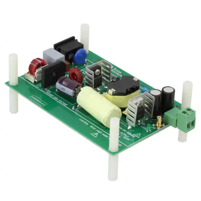
UCC28630EVM-572, 65-W Nominal, 130-W Peak,
Primary-Side Regulated Adapter Module
1
Introduction
The UCC28630EVM-572 evaluation module is a 65-W nominal, 130-W peak off-line flyback converter. It
provides constant-voltage (CV) and constant-current (CC) output regulation using the bias winding to
sense a scaled proportion of the output voltage and the primary current sense resistor to sense a scaled
version of the secondary current. Output voltage regulation within 1% is maintained down to no-load by
reducing the switching frequency and the device bias current consumption.
2
Description
This evaluation module uses the UCC28630 High-Power Flyback Controller with Primary-Side Regulation
and Peak-Power Mode in a 65-W converter to provide a regulated output voltage of 19.5 V. The input
accepts a voltage range of 90 VAC to 265 VAC. The output is designed for 19.5 V when in constant
voltage mode and 3.34-A nominal output current.
The EVM transiently delivers ~7 A of constant charge down to an output voltage of ~12 V. The unit can
only transiently operate at > 140% of the nominal output power. The operation of the overload timer is
explained in detail in the UCC28630 datasheet. Sustained operation above this power level causes the
device to inhibit switching and enter hiccup fault mode until the overload is removed.
The modulation of peak current and frequency results in excellent no-load power ( 88%
• Output Over-Load Timer
• Short Circuit Protection
• Transient Power Delivery of >130 W
• Output Over Voltage Protection
• Input Brown-Out Protection
• Fault Protections Including Over Temperature, Output Over-Voltage and Output Overload, Input
Brownout
• Class B EMI Compliance
CAUTION
High voltage levels are present on the evaluation module whenever it is
energized. Proper precautions must be taken when working with the EVM. The
large bulk capacitors, C5 and C7, and the output capacitors, C11 and C12,
must be completely discharged before the EVM can be handled. Serious injury
can occur if proper safety precautions are not followed.
SLUUAX9B – February 2014 – Revised April 2015
Submit Documentation Feedback
UCC28630EVM-572, 65-W Nominal, 130-W Peak, Primary-Side Regulated
Adapter Module
Copyright © 2014–2015, Texas Instruments Incorporated
3
�Electrical Performance Specifications
3
www.ti.com
Electrical Performance Specifications
UCC28630EVM-572 Electrical Performance Specifications
PARAMETER
TEST CONDITIONS
MIN
NOM
MAX
UNITS
90
115/230
265
VRMS
2
ARMS
63
Hz
INPUT CHARACTERISTICS
Voltage range, VIN
Maximum input current
VIN = VIN(min), IOUT = IOUT(max)
Line frequency
47
60/50
No-load power consumption VIN(min) ≤ VIN ≤ VIN(max), IOUT = 0 A
70
mW
AC turn-on voltage
80
VRMS
AC turn-off voltage
65
VRMS
OUTPUT CHARACTERISTICS
(1)
Output voltage, VOUT
VIN(min) ≤ VIN ≤ VIN(max), 0 A ≤ IOUT ≤ IOUT(nom)
18.5
19.5
20.5
V
Output load current, CV
mode
VIN(min) ≤ VIN ≤ VIN(max)
0
3.34
7
A
Output load current, CC
mode, IOUT(max)
VIN(min) ≤ VIN ≤ VIN(max)
7
7.75
A
Output voltage regulation
Line regulation: VIN(min) ≤ VIN ≤ VIN(max), 0A ≤ IOUT
≤ IOUT(nom) (3.34 A)
1%
Load Regulation: 0 A ≤ IOUT ≤ IOUT(nom) (3.34 A)
3
Output voltage ripple
VIN(min) ≤ VIN ≤ VIN(max), 0A ≤ IOUT ≤ IOUT(nom) (3.34
A)
250
Steady-state output over
current threshold, IOCC
VIN(min) ≤ VIN ≤ VIN(max)
5.25
Minimum output voltage, CC VIN(min) ≤ VIN ≤ VIN(max), IOUT = IOUT(max) (7.75 A)
mode
Transient response
undershoot
%
mVpp
IOUT = 10% - 90% IOUT(nom)
11.25
12
18.0
A
V
21.00
V
126.7
kHz
SYSTEMS CHARACTERISTICS
Switching frequency, fSW
Includes frequency dithering
Average efficiency
25%, 50%, 75%, 100% load average at nominal
input voltages
0.2
Operating temperature
(1)
4
88
%
25
ºC
Unless otherwise specified all measurements are taken at the end of a 1.8 m #18 AWG cable across a R&N measurement setup
consisting of a 10-µF aluminum electrolytic capacitor and a 1-µF high-frequency ceramic capacitor.
UCC28630EVM-572, 65-W Nominal, 130-W Peak, Primary-Side Regulated
Adapter Module
SLUUAX9B – February 2014 – Revised April 2015
Submit Documentation Feedback
Copyright © 2014–2015, Texas Instruments Incorporated
�TP2
MAG
J1
C14
1000pF
MAG
88VAC - 230VAC
0.5A - 1.5A
2
1
GND
TP3
ES1D-13-F
200V
D1
NEUTRAL
TP4
39213150000
V1
4.70
R1
C2
22µF
VDD
TP11
C1
0.33µF
3
4
F1
VDD
C3
1µF
D10
2
1
C4
0.1µF
R2
100k
ACB
L1
RLTI-1099
4.5mH
ACA
DRV
100k
R3
D2
1N4007
1000V
4
5
6
8
-
2
~
~
+
Copyright © 2014–2015, Texas Instruments Incorporated
NT1
Net-Tie
-VPRI
1
CS
SD
4
3
2
1
STARPT
GND
RLTI-1098
C7
27µF
1
L2
47.7µH
3
C6
120pF
C15
10pF
R5
1.00k
0
R6
DANGER HIGH VOLTAGE
GND
TP5
BR1
800V
VSENSE
UCC28630D
DRV
VDD
HV
U1
D3
1N4007
1000V
3
LINE
TP1
-VPRI
t°
SLUUAX9B – February 2014 – Revised April 2015
Submit Documentation Feedback
C5
100µF
RT1
470k
of net
100
R4
STARPT
R8
39k
DRV
R9
180k
C8
0805
R12
1206
R7
22.6k
MAG
Minimize copper area
-VPRI
VDC
HV
TP6
R11
47.0
STARPT
0
R20
D4
BAV70-V
R10
3.90k
100V
D5
D6
C16
10pF
4.7
R13
MAG
R15
100k
1
+VSW
MURS160-13-F
CS
D9
1SMB5949BT3G
100V
D8
1SMB5947BT3G
82V
2
2
6
1
5
4
R16
0.2
11
10
9
8
also High voltage Net
of VSW net
Minimize copper area
RLTI-1100
T1
TP7
GND
Q1
STF13NM60ND
600V
-VPRI
-VPRI
3
C10
0603
R17
1206
NTST30100CTG
100V
D7
C9
2200pF
-VPRI
Connect 2 pins
of bobbin to
Vsec and Ret nets
VSEC
RET
C11
680µF
R18
8.20k
LED1
Green
TP8
TP9
RET
TP10
+VOUT
C13
1µF
+VOUT
+VOUT
1
C12
680µF
J2
OUTPUT R/A
SOCKET
1
2
18.5V - 20.5V
0A - 7A
4
2
3
4
5
J4
www.ti.com
Schematic
Schematic
Figure 1. Typical Application Circuit for 19.5-V, 65-W Adapter
UCC28630EVM-572, 65-W Nominal, 130-W Peak, Primary-Side Regulated
Adapter Module
5
�Test Setup - No Load
5
www.ti.com
Test Setup - No Load
Figure 2 shows the equipment setup when testing at no load. It is important to note in this setup that the
current flowing through the input impedance of the voltmeter does not flow through shunt resistor which is
used to measure the input current of the EVM. This is important because a power meter having an input
impedance of 1 MΩ draws a current of 230 μA at 230 VRMS. This equates to a power dissipation of ~59
mW, it is important that this current is not measured as EVM input current.
Also, do not connect the oscilloscope probes or any other sensing devices to the unit while measuring noload power as these can provide a path for common mode current to flow. This causes an error in the
measurement.
During the no-load test, the power analyzer should be set for long-averaging mode in order to include
several cycles of operation and an appropriate current scale factor when using an external shunt.
Alternatively a power meter with an internal shunt can be used but it must be configured such that the
shunt current is not supplied in series with the EVM input current.
AC SOURCE
-
+
-
-
+
+
VLO ALO AHI Aext
+
VHI
POWER METER
Figure 2. Test Setup
6
UCC28630EVM-572, 65-W Nominal, 130-W Peak, Primary-Side Regulated
Adapter Module
SLUUAX9B – February 2014 – Revised April 2015
Submit Documentation Feedback
Copyright © 2014–2015, Texas Instruments Incorporated
�Test Setup with EVM Under Load
www.ti.com
6
Test Setup with EVM Under Load
Figure 3 shows the equipment test setup when testing with load. Here the voltage sense has been moved
to the other side of the shunt resistance This is because the error in the input current reading caused by
the input impedance of the voltmeter reduces as the input current increases.
However as the input current increases, the voltage drop across the current shunt causes an error in the
voltage measurement with the setup shown in Figure 3. Moving the VLO connection to the opposite side
of the shunt as shown removes this error.
AC SOURCE
-
+
DMM V1
Electronic
Load
DMM A1
Oscilloscope
+
-
Aext ALO AHI VHI
VLO
+
-
+
POWER METER
Figure 3. Test Setup
NOTE: This setup can also be used for no-load testing as long as the power consumption of the
voltmeter is subtracted from the power meter reading.
SLUUAX9B – February 2014 – Revised April 2015
Submit Documentation Feedback
UCC28630EVM-572, 65-W Nominal, 130-W Peak, Primary-Side Regulated
Adapter Module
Copyright © 2014–2015, Texas Instruments Incorporated
7
�Test Setup with EVM Under Load
6.1
www.ti.com
Test Equipment
AC Voltage Source: The input source shall be an isolated variable AC source capable of supplying
between 90 VAC and 265 VAC at no less than 200 W and connected as shown in Figure 2 and Figure 3.
For accurate efficiency calculations, a power meter should be inserted between the AC source and the
EVM as shown in Figure 2 and Figure 3.
Output Load: A programmable electronic load capable of sinking 0 A to 10 A shall be used. For constant
current mode testing of the EVM, the electronic load should be set to constant resistance mode.
Power Meter: A power analyzer shall be capable of measuring low input power, typically less than 5 mW
and a long averaging mode, if low-power standby mode input-power measurements are to be taken.
Multimeters: For highest accuracy, VOUT can be monitored by connecting a DC voltmeter, DMM V1,
directly across the +VOUT and –VOUT terminals as shown in Figure 3. A DC current meter, DMM A1,
should be placed in series with the electronic load for accurate output current measurements.
Oscilloscope: A digital or analog oscilloscope with 500-MHz scope probes is recommended.
Fan: Forced air cooling is not required at the nominal operating point of 65-W load. If the unit is to be run
in sustained overload (>100% PNOM) a fan is required.
Recommended Wire Gauge: a minimum of AWG #18 wire is recommended on the input. The wire
connections between the AC source and the EVM, should be less than two feet long.
A 1.8m #18 AWG cable is recommended on the output.
WARNING
High voltages that may cause injury exist on this evaluation
module (EVM). Please ensure safety procedures are followed when
working on this EVM. Never leave a powered EVM unattended.
6.2
List of Test Points
Test Point Functional Description
TEST POINT
8
NAME
DESCRIPTION
TP1
Live
Live terminal of the AC input
TP2
Mag
Positive end of VBIAS (magnetic sense) winding
TP3, TP5, TP7
GND / -VPRI
TP4
Neutral
TP6
HV
TP8, TP9
Secondary ground / Ret
TP10
+VOUT
Positive terminal of the output voltage
TP11
VDD
Bias voltage of the device.
Primary-side ground
Neutral terminal of the AC input
Positive terminal of bulk capacitor
Secondary-side ground
UCC28630EVM-572, 65-W Nominal, 130-W Peak, Primary-Side Regulated
Adapter Module
SLUUAX9B – February 2014 – Revised April 2015
Submit Documentation Feedback
Copyright © 2014–2015, Texas Instruments Incorporated
�Test Setup with EVM Under Load
www.ti.com
6.3
Applying Power to the EVM
1. Set up the EVM as shown in Figure 3.
2. Set the electronic load to the desired setting. If testing the constant current characteristic of the unit,
set the load to constant resistance mode.
3. Set the AC source voltage between 90 VAC and 265 VAC.
4. Monitor the output voltage on DMM V1.
5. Monitor the output current on DMM A1.
6.4
No-Load Power Consumption
1. Use the test setup shown in Figure 3.
(a) Set the power analyzer for long-averaging time or integration mode (to include several cycles of
operation) and the appropriate setup for measuring no-load power.
(b) Allow the unit run at the line voltage where the no-load power will be measured for ~5 minutes. This
is to allow the leakage current of the high-voltage bulk capacitors to decay to the steady-state
value.
2. Apply power to the EVM per Section 6.4.
3. Monitor the input power on the power analyzer while varying the input voltage.
4. Make sure the EVM is off and the bulk capacitors and output capacitors are completely discharged
before handling the EVM.
6.5
Line/Load Regulation and Efficiency Measurement Procedure
1. For load regulation, use the test set up shown in Figure 3.
(a) Set the power analyzer to normal mode.
(b) Set the AC source to a constant voltage between 90 VAC and 265 VAC.
(c) Vary the load so that the output current varies from 0 A up to 3.34 A, as measured on DMM A1.
(d) Observe that the output voltage on DMM V1 remains within 3% of the 19.5 V constant voltage
regulation value.
(e) Observe that if the constant resistance level of the electronic load is decreased lower than the
maximum load value, the EVM maintains constant current regulation within 10% of the constant
current limit until the bias voltage drops below bias UV. As mentioned above, the EVM can only
operate in this region transiently. The delay before the overload timer trips depends on the state of
the timer before entering the overload region. Refer to the UCC28630 datasheet, (TI Literature
Number SLUSBW3). The EVM automatically restarts after 1 s.
2. For line regulation, use the test setup shown in Figure 3
(a) Set the load to IOUT(nom)
(b) Vary the AC source from 90 VAC to 265 VAC
(c) Observe that the output voltage on DMM V1 stays within 3% of the 19.5 V constant voltage
regulation value.
6.6
Output Voltage Ripple
An external 10-µF aluminum capacitor and 1-µF ceramic noise decoupling capacitor network should be
connected to the output to measure the output ripple and noise. This network should be connected to the
end of the cable specified above (Section 3) but can be clipped across the test points on +VOUT and RTN
if desired for convenience. The loop area between the scope probe tip and ground should be minimized
for accurate ripple and noise measurements.
6.7
Equipment Shutdown
1. To quickly discharge the output and bulk capacitors, make sure there is a load greater than 1 A on the
EVM.
2. Turn off the AC source.
SLUUAX9B – February 2014 – Revised April 2015
Submit Documentation Feedback
UCC28630EVM-572, 65-W Nominal, 130-W Peak, Primary-Side Regulated
Adapter Module
Copyright © 2014–2015, Texas Instruments Incorporated
9
�Performance Data and Typical Characteristic Curves
7
www.ti.com
Performance Data and Typical Characteristic Curves
Figure 4 through Figure 14 present typical performance curves for UCC28630EVM-572.
7.1
Efficiency
The average efficiency at 115-VAC, 60-Hz nominal input and 230-VAC, 50-Hz nominal input exceeds 88%
efficiency at the end of the cable as specified in . Further increases in efficiency could be achieved with a
transformer made with an increased core size and by designing for a lower peak power.
89.5
115 V Eff(%)
230 V Eff(%)
89.25
89
88.75
Efficiency (%)
88.5
88.25
88
87.75
87.5
87.25
87
86.75
86.5
5
10
15
20
25
30 35 40 45
Output Power (W)
50
55
60
65
D001
Figure 4. UCC28630EVM-572 Efficiency
Table 1. Average Efficiency
AVERAGE EFFICIENCY TEST
VIN (V)
115
230
10
F (Hz)
60
50
POUT (W)
EFFICIENCY
(%)
7.324
6.45
88.13
17.78
15.90
89.41
50
35.89
31.92
88.95
75
54.37
47.74
87.81
100
72.62
63.14
86.95
10
7.409
6.43
86.73
25
17.81
15.85
89.02
50
35.69
31.82
89.16
75
53.6
47.54
88.70
100
71.38
62.86
88.07
% LOAD
PIN (W)
10
25
UCC28630EVM-572, 65-W Nominal, 130-W Peak, Primary-Side Regulated
Adapter Module
AVG
EFFICIENCY
(%)
SPEC (%)
79
88.28
88
79
88.74
88
SLUUAX9B – February 2014 – Revised April 2015
Submit Documentation Feedback
Copyright © 2014–2015, Texas Instruments Incorporated
�Performance Data and Typical Characteristic Curves
www.ti.com
7.2
Load Regulation – Including Output Cable Drop
Figure 5. UCC28630EVM-572 Measured Load and Line Regulation at Cable End
7.3
Load Regulation – Not Including Output Cable Drop
Figure 6. UCC28630EVM-572 Measured Load and Line Regulation at PCB End
SLUUAX9B – February 2014 – Revised April 2015
Submit Documentation Feedback
UCC28630EVM-572, 65-W Nominal, 130-W Peak, Primary-Side Regulated
Adapter Module
Copyright © 2014–2015, Texas Instruments Incorporated
11
�Performance Data and Typical Characteristic Curves
7.4
www.ti.com
No-Load Power Consumption
No-load power consumption measured less than 70 mW over the entire line input range.
UCC28630EVM-572 No-Load Power Consumption
7.5
VIN (V)
F (Hz)
PIN (W) MEASURED
PIN (W) MAX SPEC
VOUT (V)(Load_1)
115
60
0.057
0.070
19.58
230
50
0.060
0.070
19.69
Output Voltage vs Output Current
The curves in Figure 7 are generated by running the converter in constant-voltage mode at 100-mA load
in steady state. The load resistance is then pulsed for 20 ms every second to increase the load current.
Once load constant-current threshold is reached, the converter transitions into constant-current mode
where the load current is regulated until the bias voltage falls below the bias UV threshold (~8.0 V), at
which point the converter shuts down. The unit then enters hiccup mode until the load is decreased
(resistance is increased).
Figure 7. UCC28630EVM-572 Output Voltage as a Function of Load Current
12
UCC28630EVM-572, 65-W Nominal, 130-W Peak, Primary-Side Regulated
Adapter Module
SLUUAX9B – February 2014 – Revised April 2015
Submit Documentation Feedback
Copyright © 2014–2015, Texas Instruments Incorporated
�Performance Data and Typical Characteristic Curves
www.ti.com
7.6
Transient Response
The transient response shown in Figure 8 and Figure 9 was taken with a load transition from 10% to 90%
of full load.
• Channel 1 is the output voltage at 2-V per division. The cursors show the transient response
specification limits of 18 V and 21 V.
• Channel 2 shows the input line voltage.
• Channel 3 is the output current on a scale of 1-A per division.
Figure 8. UCC28630EVM-572 Load Transient
(10% to 90% Full Load Transient at 230 V)
SLUUAX9B – February 2014 – Revised April 2015
Submit Documentation Feedback
Figure 9. UCC28630EVM-572 Load Transient
(10% to 90% Full Load Transient at 230 VAC)
UCC28630EVM-572, 65-W Nominal, 130-W Peak, Primary-Side Regulated
Adapter Module
Copyright © 2014–2015, Texas Instruments Incorporated
13
�Performance Data and Typical Characteristic Curves
7.7
www.ti.com
Output Ripple
Figure 10 and Figure 11 shows the output voltage ripple, measured across the noise decoupling caps at
the end of the cable.
• Channel 1 is the output voltage at 200-mV per division. The cursors show the output ripple
specification limits of 600 mV pk-pk
• Channel 2 shows the input line voltage.
• Channel 3 is the output current on a scale of 1-A per division.
Figure 10. UCC28630EVM-572 Output Ripple and Noise
(90 V/50 Hz, Load = 65 W)
14
Figure 11. UCC28630EVM-572 Output Ripple and Noise
(230 V/63 Hz, Load = 65 W)
UCC28630EVM-572, 65-W Nominal, 130-W Peak, Primary-Side Regulated
Adapter Module
SLUUAX9B – February 2014 – Revised April 2015
Submit Documentation Feedback
Copyright © 2014–2015, Texas Instruments Incorporated
�Performance Data and Typical Characteristic Curves
www.ti.com
7.8
Turn-On Waveform
Figure 12 shows the output voltage at turn on under full load conditions with an input voltage of 230 VAC,
50 Hz.
VBIAS is charged via the internal high-voltage start-up FET until it reaches the VBIAS turn-on threshold of ~15
V.
The device enables the gate drive and charges the output voltage. During the initial period of this charging
the bias capacitor supplies the device and gate-drive currents so the bias voltage falls.
When the rectified bias-winding voltage exceeds the bias-capacitor voltage, the supply current is supplied
from the winding and the bias voltage is maintained at ~12.5 V.
Figure 12. Output Voltage Turn-On Waveform
SLUUAX9B – February 2014 – Revised April 2015
Submit Documentation Feedback
UCC28630EVM-572, 65-W Nominal, 130-W Peak, Primary-Side Regulated
Adapter Module
Copyright © 2014–2015, Texas Instruments Incorporated
15
�Performance Data and Typical Characteristic Curves
7.9
www.ti.com
Bias Winding and VSENSE Pin Voltage
NB: Probing the VSENSE pin voltage adds capacitance to the pin and affects the voltage sampled by the
device, This affects the output voltage regulation. Probing the VSENSE pin is not recommended in normal
operation or during testing.
Figure 13. Bias Winding and VSENSE Pin Voltage Waveforms
7.10 Switching Node and Current Sense Waveforms
Figure 14. Drain and CS Voltages
16
UCC28630EVM-572, 65-W Nominal, 130-W Peak, Primary-Side Regulated
Adapter Module
SLUUAX9B – February 2014 – Revised April 2015
Submit Documentation Feedback
Copyright © 2014–2015, Texas Instruments Incorporated
�Performance Data and Typical Characteristic Curves
www.ti.com
7.11 EMI Plots
Figure 15. 115-VAC Conducted Emissions Plot
Figure 16. 230-VAC Conducted Emissions Plot
SLUUAX9B – February 2014 – Revised April 2015
Submit Documentation Feedback
UCC28630EVM-572, 65-W Nominal, 130-W Peak, Primary-Side Regulated
Adapter Module
Copyright © 2014–2015, Texas Instruments Incorporated
17
�EVM Assembly Drawing and PCB Layout
8
www.ti.com
EVM Assembly Drawing and PCB Layout
The following figures (Figure 17 through Figure 20) show the design of the UCC28630EVM-572 printed
circuit board.
Figure 17. UCC28630EVM-572 Top Layer Assembly Drawing (top view)
Figure 18. UCC28630EVM-572 Bottom Layer Assembly Drawing (bottom view)
18
UCC28630EVM-572, 65-W Nominal, 130-W Peak, Primary-Side Regulated
Adapter Module
SLUUAX9B – February 2014 – Revised April 2015
Submit Documentation Feedback
Copyright © 2014–2015, Texas Instruments Incorporated
�EVM Assembly Drawing and PCB Layout
www.ti.com
Figure 19. UCC28630EVM-572 Top Copper (top view)
Figure 20. UCC28630EVM-572 Bottom Copper (bottom view)
SLUUAX9B – February 2014 – Revised April 2015
Submit Documentation Feedback
UCC28630EVM-572, 65-W Nominal, 130-W Peak, Primary-Side Regulated
Adapter Module
Copyright © 2014–2015, Texas Instruments Incorporated
19
�List of Materials
www.ti.com
9
List of Materials
9.1
Transformer Information
9.1.1
•
•
•
•
•
•
•
9.1.2
Materials
Ferroxcube RM10/1 core set 3C95 material of equivalent, 225 nH aluminum.
Ferroxcube CPV-RM10/1-1S-12PD coil former or equivalent.
15 strands of 0.1 mm ECW twisted, 100 turns/meter.
0.2 mm ECW.
7 mm x 0.2 mm Furukawa TEX-E triple insulated wire or equivalent.
1 oz (66 µm thick) adhesive copper foil.
Mylar tape.
Construction
xxxxxxxxxxx
xxxxxxxxxxx
xxxxxxxxxxx
xxxxxxxxxxx
xxxxxxxxxxx
xxxxxxxxxxx
Pin Number
6
VBULK
VBIAS
VSEC
VBIAS
VSW
W5 t 17T - 15*0.1mm ECW
1
10,11
8,9
2
-VPRI
5
W3 t 6T - 7*0.2mm TEX-E
Ret
1
4
W4 t 1T - 1Oz Copper Foil
5
W2* t 4T - 7*0.2mm ECW
+ 2T, 5*0.2mm ECW
W1 t 17T - 15*0.1mm ECW
Figure 21. Transformer Construction
•
•
•
•
•
•
W1, One layer across bobbin. Return at 90º to pin 5. One layer of mylar tape over winding.
W2, Return two strands of W2 to pin 2 after 4 turns. The other five strands can be cut and left floating
after six turns. W2 is to act as a shield so the strands should be evenly spaced across the winding
window. One layer of mylar tape over winding.
W3, start one strand at pin 8 and one strand at pin 9, wind byfilar in a single layer across the winding
window. Leave ends floating.
W4 is a copper foil shield the width of the winding window. This shield should be covered with tape
which folds over the edges of the foil. The middle of the winding is connected to pin 1. The two ends
should be taped/cut so that they do not short. One layer of mylar tape over winding.
W5, One layer across bobbin. Return at 90º to pin 6. One layer of mylar tape over winding.
Return ends of W3 to pins 10 and 11.
NOTE: Depending on the safety requirements of the design it may be necessary to terminate the
ends of W3 in the PCB as flying leads (rather than terminating them on the bobbin) to
increase the spacing from the exposed secondary to the primary referenced core.
•
•
•
•
20
Two layers of mylar tape on top.
One layer of copper tape around assembled core, connect to pin 2.
Cover copper tape with Mylar tape.
Varnish completed assembly.
UCC28630EVM-572, 65-W Nominal, 130-W Peak, Primary-Side Regulated
Adapter Module
SLUUAX9B – February 2014 – Revised April 2015
Submit Documentation Feedback
Copyright © 2014–2015, Texas Instruments Incorporated
�List of Materials
www.ti.com
Detailed List of Materials
Table 2 EVM component list according to the schematic shown in Figure 12.
Table 2. UCC28630EVM-572 List of Materials
QTY
DES
DESCRIPTION
MANUFACTURER
PART NUMBER
1
BR1
Diode, switching-bridge, 800 V, 4 A, TH
VishaySemiconductor
GBU4K-E3/45
1
C1
Capacitor, film, 0.33 µF, 630 V, ±20%, TH
VishayBccomponents
BFC233840334
1
C2
Capacitor, aluminum, 22 µF, 25 V, ±20%, TH
Rubycon
25ML22MEFC5X5
1
C3
Capacitor, ceramic, 1 µF, 25 V, ±10%, X7R, 1206
AVX
12063C105KAT2A
1
C4
Capacitor, ceramic, 0.1 µF, 25 V, ±10%, X7R, 0603 Kemet
C0603C104K3RACTU
1
C5
Capacitor, aluminum, 100 µF, 400 V, ±20%, TH
Rubycon
400KXW100MEFC16X3
0
1
C6
Capacitor, ceramic, 120 pF, 50 V, ±5%, C0G/NP0,
0603
AVX
06035A121JAT2A
1
C7
Capacitor, aluminum, 27 µF, 400 V, ±20%, TH
Nichicon
UCY2G270MHD1TO
1
C9
Capacitor, ceramic, 2200 pF, 250 V, ±20%, E, Disc MuRata
10mm x 8 mm
DE1E3KX222MA5BA01
2
C11, C12
Capacitor, aluminum, 680 µF, 35 V, ±20%, 0.019
Ω, TH
Nichicon
UHW1V681MPD6
1
C13
Capacitor, ceramic, 1 µF, 50 V, ±10%, X7R, 0805
AVX
08055C105KAT2A
1
C14
Capacitor, ceramic, 1000 pF, 100 V, ±10%, X7R,
0805
AVX
08051C102KAT2A
1
C15
Capacitor, ceramic, 10 pF, 50 V, ±5%, C0G/NP0,
0603
AVX
06035A100JAT2A
1
C16
Capacitor, ceramic, 10 pF, 200 V, ±5%, C0G/NP0,
1206
AVX
12062A100JAT2A
1
D1
Diode, ultrafast, 200 V, 1 A, SMA
Diodes Inc.
ES1D-13-F
2
D2, D3
Diode, P-N, 1000 V, 1 A, TH
Fairchild
Semiconductor
1N4007
1
D4
Diode, switching, 70 V, 0.25 A, SOT-23
VishaySemiconductor
BAV70-V
1
D5
Diode, ultrafast, 100 V, 0.25 A, SOD-323
NXP Semiconductor
BAS316,115
1
D6
Diode, ultrafast, 600 V, 1 A, SMB
Diodes Inc.
MURS160-13-F
1
D7
Diode, Schottky, 100 V, 15 A, TH
ON Semiconductor
NTST30100CTG
1
D8
Diode, Zener, 82 V, 550 mW, SMB
ON Semiconductor
1SMB5947BT3G
1
D9
Diode, Zener, 100 V, 550 mW, SMB
ON Semiconductor
1SMB5949BT3G
1
F1
Fuse, 3.15 A, 250 V, TH
Littelfuse
39213150000
4
H1, H2, H5, H6
Standoff, Hex, 1"L #6-32 nylon, M-F
Keystone
4820
4
H3, H4, H7, H8
Standoff, Hex, 1"L #4-40 nylon
Keystone
1902E
2
H10, H13
Machine screw pan phillips, 5/16", 4-40
B-F Fastener Supply
PMSSS 440 0031 PH
2
H11, H14
Washer, split lock, #4
Keystone
4693
2
H12, H15
Nut, Hex, 1/4" Thick, #4-40
B-F Fastener Supply
HNSS440
2
HS1, HS2
Board level heatsink .375" TO-220
Aavid Thermalloy
7173DG
1
J1
AC receptacle, 2.5 A, R/A, TH
Qualtek Electronics
Corporation
770W-X2/10
1
J2
Terminal block, 2 x 1, 5.08 mm, TH
FCI
20020110-H021A01LF
1
J3
Terminal block plug 2 positive 5.08MM
FCI
20020006-H021B01LF
1
J4
Connector, SMB, vertical RCP 0 to 4 GHz, 50 Ω,
TH
Emerson Network
Power
131-3701-261
1
L1
Inductor, toroid, 4.5 mH, A, 0.05 Ω, TH
Renco Electronics
RLTI-1099
1
L2
Inductor, toroid,, 47.7 µH, A, 0.04 Ω, TH
Renco Electronics
RLTI-1098
1
LED1
LED, green, TH
Everlight
HLMP1523
SLUUAX9B – February 2014 – Revised April 2015
Submit Documentation Feedback
UCC28630EVM-572, 65-W Nominal, 130-W Peak, Primary-Side Regulated
Adapter Module
Copyright © 2014–2015, Texas Instruments Incorporated
21
�Revision History
www.ti.com
Table 2. UCC28630EVM-572 List of Materials (continued)
QTY
DES
DESCRIPTION
MANUFACTURER
PART NUMBER
1
Q1
MOSFET, N-channel, 600 V, 11 A, TO-220
FullPAK
ST Microelectronics
STF13NM60ND
1
R1
Resistor, 4.70 Ω, 1%, 0.125 W, 0805
Panasonic
ERJ-6RQF4R7V
2
R2, R3
Resistor, 100 kΩ, 1%, 0.25 W, 1206
Yageo America
RC1206FR-07100KL
1
R4
Resistor, 100 Ω, 1%, 0.1 W, 0603
Vishay-Dale
CRCW0603100RFKEA
1
R5
Resistor, 1.00 kΩ, 1%, 0.1 W, 0603
Vishay-Dale
CRCW06031K00FKEA
1
R6
Resistor, 0 Ω, 5%, 0.1 W, 0603
Vishay-Dale
CRCW06030000Z0EA
1
R7
Resistor, 22.6 kΩ, 1%, 0.25 W, 1206
Vishay-Dale
CRCW120622K6FKEA
1
R8
Resistor, 39 kΩ, 5%, 0.25 W, 1206
Vishay-Dale
CRCW120639K0JNEA
1
R9
Resistor, 180 kΩ, 1%, 0.1 W, 0603
Yageo America
RC0603FR-07180KL
1
R10
Resistor, 3.90 kΩ, 1%, 0.1 W, 0603
Yageo America
RC0603FR-073K9L
1
R11
Resistor, 47.0 Ω, 1%, 0.25 W, 1206
Yageo America
RC1206FR-0747RL
1
R13
Resistor, 4.7 Ω, 5%, 0.25 W, 1206
Vishay-Dale
CRCW12064R70JNEA
1
R15
Resistor, 100 kΩ, 1%, 0.1 W, 0603
Vishay-Dale
CRCW0603100KFKEA
1
R16
Resistor, 0.2 Ω, 1%, 2 W, 2512
Stackpole Electronics
Inc
CSRN2512FKR200
1
R18
Resistor, 8.20 kΩ, 1%, 0.25 W, 1206
Yageo America
RC1206FR-078K2L
1
R20
Resistor, 0 Ω, 5%, 0.25 W, 1206
Vishay-Dale
CRCW12060000Z0EA
1
RT1
Thermistor NTC, 470 , 5%, disc, 5.5 mm x 5 mm
EPCOS Inc
B57164K474J
1
T1
Transformer, 260 µH, TH
Renco Electronics
RLTI-1100
5
TP1, TP4, TP6,
TP10, TP11
Test point, compact, red, TH
Keystone
5005
1
TP2
Test point, compact, white, TH
Keystone
5007
5
TP3, TP5, TP7,
TP8, TP9
Test point, compact, black, TH
Keystone
5006
1
U1
Green-Mode Flyback Controller, D0007A
Texas Instruments
UCC28630D
1
V1
Varistor, 430 V, 4.5KA, TH
EPCOS Inc
B72214S0271K101
Revision History
Changes from Original (February 2014) to A Revision .................................................................................................. Page
•
Changed the Typical Application Circuit. ............................................................................................... 5
Changes from A Revision (May 2014) to B Revision ...................................................................................................... Page
•
•
•
•
•
Added new Test Setup - No Load image. .............................................................................................. 6
Added new Test Setup with EVM Under Load image. ............................................................................... 7
Changed Efficiency section with new iUCC28630EVM-572 Efficiency image and Average Efficiency table. ............... 10
Added EMI Plots section. ............................................................................................................... 17
Added Transformer Information section............................................................................................... 20
NOTE: Page numbers for previous revisions may differ from page numbers in the current version.
22
Revision History
SLUUAX9B – February 2014 – Revised April 2015
Submit Documentation Feedback
Copyright © 2014–2015, Texas Instruments Incorporated
�STANDARD TERMS AND CONDITIONS FOR EVALUATION MODULES
1.
Delivery: TI delivers TI evaluation boards, kits, or modules, including any accompanying demonstration software, components, or
documentation (collectively, an “EVM” or “EVMs”) to the User (“User”) in accordance with the terms and conditions set forth herein.
Acceptance of the EVM is expressly subject to the following terms and conditions.
1.1 EVMs are intended solely for product or software developers for use in a research and development setting to facilitate feasibility
evaluation, experimentation, or scientific analysis of TI semiconductors products. EVMs have no direct function and are not
finished products. EVMs shall not be directly or indirectly assembled as a part or subassembly in any finished product. For
clarification, any software or software tools provided with the EVM (“Software”) shall not be subject to the terms and conditions
set forth herein but rather shall be subject to the applicable terms and conditions that accompany such Software
1.2 EVMs are not intended for consumer or household use. EVMs may not be sold, sublicensed, leased, rented, loaned, assigned,
or otherwise distributed for commercial purposes by Users, in whole or in part, or used in any finished product or production
system.
2
Limited Warranty and Related Remedies/Disclaimers:
2.1 These terms and conditions do not apply to Software. The warranty, if any, for Software is covered in the applicable Software
License Agreement.
2.2 TI warrants that the TI EVM will conform to TI's published specifications for ninety (90) days after the date TI delivers such EVM
to User. Notwithstanding the foregoing, TI shall not be liable for any defects that are caused by neglect, misuse or mistreatment
by an entity other than TI, including improper installation or testing, or for any EVMs that have been altered or modified in any
way by an entity other than TI. Moreover, TI shall not be liable for any defects that result from User's design, specifications or
instructions for such EVMs. Testing and other quality control techniques are used to the extent TI deems necessary or as
mandated by government requirements. TI does not test all parameters of each EVM.
2.3 If any EVM fails to conform to the warranty set forth above, TI's sole liability shall be at its option to repair or replace such EVM,
or credit User's account for such EVM. TI's liability under this warranty shall be limited to EVMs that are returned during the
warranty period to the address designated by TI and that are determined by TI not to conform to such warranty. If TI elects to
repair or replace such EVM, TI shall have a reasonable time to repair such EVM or provide replacements. Repaired EVMs shall
be warranted for the remainder of the original warranty period. Replaced EVMs shall be warranted for a new full ninety (90) day
warranty period.
3
Regulatory Notices:
3.1 United States
3.1.1
Notice applicable to EVMs not FCC-Approved:
This kit is designed to allow product developers to evaluate electronic components, circuitry, or software associated with the kit
to determine whether to incorporate such items in a finished product and software developers to write software applications for
use with the end product. This kit is not a finished product and when assembled may not be resold or otherwise marketed unless
all required FCC equipment authorizations are first obtained. Operation is subject to the condition that this product not cause
harmful interference to licensed radio stations and that this product accept harmful interference. Unless the assembled kit is
designed to operate under part 15, part 18 or part 95 of this chapter, the operator of the kit must operate under the authority of
an FCC license holder or must secure an experimental authorization under part 5 of this chapter.
3.1.2
For EVMs annotated as FCC – FEDERAL COMMUNICATIONS COMMISSION Part 15 Compliant:
CAUTION
This device complies with part 15 of the FCC Rules. Operation is subject to the following two conditions: (1) This device may not
cause harmful interference, and (2) this device must accept any interference received, including interference that may cause
undesired operation.
Changes or modifications not expressly approved by the party responsible for compliance could void the user's authority to
operate the equipment.
FCC Interference Statement for Class A EVM devices
NOTE: This equipment has been tested and found to comply with the limits for a Class A digital device, pursuant to part 15 of
the FCC Rules. These limits are designed to provide reasonable protection against harmful interference when the equipment is
operated in a commercial environment. This equipment generates, uses, and can radiate radio frequency energy and, if not
installed and used in accordance with the instruction manual, may cause harmful interference to radio communications.
Operation of this equipment in a residential area is likely to cause harmful interference in which case the user will be required to
correct the interference at his own expense.
SPACER
SPACER
SPACER
SPACER
SPACER
SPACER
SPACER
SPACER
�FCC Interference Statement for Class B EVM devices
NOTE: This equipment has been tested and found to comply with the limits for a Class B digital device, pursuant to part 15 of
the FCC Rules. These limits are designed to provide reasonable protection against harmful interference in a residential
installation. This equipment generates, uses and can radiate radio frequency energy and, if not installed and used in accordance
with the instructions, may cause harmful interference to radio communications. However, there is no guarantee that interference
will not occur in a particular installation. If this equipment does cause harmful interference to radio or television reception, which
can be determined by turning the equipment off and on, the user is encouraged to try to correct the interference by one or more
of the following measures:
•
•
•
•
Reorient or relocate the receiving antenna.
Increase the separation between the equipment and receiver.
Connect the equipment into an outlet on a circuit different from that to which the receiver is connected.
Consult the dealer or an experienced radio/TV technician for help.
3.2 Canada
3.2.1
For EVMs issued with an Industry Canada Certificate of Conformance to RSS-210
Concerning EVMs Including Radio Transmitters:
This device complies with Industry Canada license-exempt RSS standard(s). Operation is subject to the following two conditions:
(1) this device may not cause interference, and (2) this device must accept any interference, including interference that may
cause undesired operation of the device.
Concernant les EVMs avec appareils radio:
Le présent appareil est conforme aux CNR d'Industrie Canada applicables aux appareils radio exempts de licence. L'exploitation
est autorisée aux deux conditions suivantes: (1) l'appareil ne doit pas produire de brouillage, et (2) l'utilisateur de l'appareil doit
accepter tout brouillage radioélectrique subi, même si le brouillage est susceptible d'en compromettre le fonctionnement.
Concerning EVMs Including Detachable Antennas:
Under Industry Canada regulations, this radio transmitter may only operate using an antenna of a type and maximum (or lesser)
gain approved for the transmitter by Industry Canada. To reduce potential radio interference to other users, the antenna type
and its gain should be so chosen that the equivalent isotropically radiated power (e.i.r.p.) is not more than that necessary for
successful communication. This radio transmitter has been approved by Industry Canada to operate with the antenna types
listed in the user guide with the maximum permissible gain and required antenna impedance for each antenna type indicated.
Antenna types not included in this list, having a gain greater than the maximum gain indicated for that type, are strictly prohibited
for use with this device.
Concernant les EVMs avec antennes détachables
Conformément à la réglementation d'Industrie Canada, le présent émetteur radio peut fonctionner avec une antenne d'un type et
d'un gain maximal (ou inférieur) approuvé pour l'émetteur par Industrie Canada. Dans le but de réduire les risques de brouillage
radioélectrique à l'intention des autres utilisateurs, il faut choisir le type d'antenne et son gain de sorte que la puissance isotrope
rayonnée équivalente (p.i.r.e.) ne dépasse pas l'intensité nécessaire à l'établissement d'une communication satisfaisante. Le
présent émetteur radio a été approuvé par Industrie Canada pour fonctionner avec les types d'antenne énumérés dans le
manuel d’usage et ayant un gain admissible maximal et l'impédance requise pour chaque type d'antenne. Les types d'antenne
non inclus dans cette liste, ou dont le gain est supérieur au gain maximal indiqué, sont strictement interdits pour l'exploitation de
l'émetteur
3.3 Japan
3.3.1
Notice for EVMs delivered in Japan: Please see http://www.tij.co.jp/lsds/ti_ja/general/eStore/notice_01.page 日本国内に
輸入される評価用キット、ボードについては、次のところをご覧ください。
http://www.tij.co.jp/lsds/ti_ja/general/eStore/notice_01.page
3.3.2
Notice for Users of EVMs Considered “Radio Frequency Products” in Japan: EVMs entering Japan may not be certified
by TI as conforming to Technical Regulations of Radio Law of Japan.
If User uses EVMs in Japan, not certified to Technical Regulations of Radio Law of Japan, User is required by Radio Law of
Japan to follow the instructions below with respect to EVMs:
1.
2.
3.
Use EVMs in a shielded room or any other test facility as defined in the notification #173 issued by Ministry of Internal
Affairs and Communications on March 28, 2006, based on Sub-section 1.1 of Article 6 of the Ministry’s Rule for
Enforcement of Radio Law of Japan,
Use EVMs only after User obtains the license of Test Radio Station as provided in Radio Law of Japan with respect to
EVMs, or
Use of EVMs only after User obtains the Technical Regulations Conformity Certification as provided in Radio Law of Japan
with respect to EVMs. Also, do not transfer EVMs, unless User gives the same notice above to the transferee. Please note
that if User does not follow the instructions above, User will be subject to penalties of Radio Law of Japan.
SPACER
SPACER
SPACER
SPACER
SPACER
�【無線電波を送信する製品の開発キットをお使いになる際の注意事項】 開発キットの中には技術基準適合証明を受けて
いないものがあります。 技術適合証明を受けていないもののご使用に際しては、電波法遵守のため、以下のいずれかの
措置を取っていただく必要がありますのでご注意ください。
1.
2.
3.
電波法施行規則第6条第1項第1号に基づく平成18年3月28日総務省告示第173号で定められた電波暗室等の試験設備でご使用
いただく。
実験局の免許を取得後ご使用いただく。
技術基準適合証明を取得後ご使用いただく。
なお、本製品は、上記の「ご使用にあたっての注意」を譲渡先、移転先に通知しない限り、譲渡、移転できないものとします。
上記を遵守頂けない場合は、電波法の罰則が適用される可能性があることをご留意ください。 日本テキサス・イ
ンスツルメンツ株式会社
東京都新宿区西新宿6丁目24番1号
西新宿三井ビル
3.3.3
Notice for EVMs for Power Line Communication: Please see http://www.tij.co.jp/lsds/ti_ja/general/eStore/notice_02.page
電力線搬送波通信についての開発キットをお使いになる際の注意事項については、次のところをご覧くださ
い。http://www.tij.co.jp/lsds/ti_ja/general/eStore/notice_02.page
SPACER
4
EVM Use Restrictions and Warnings:
4.1 EVMS ARE NOT FOR USE IN FUNCTIONAL SAFETY AND/OR SAFETY CRITICAL EVALUATIONS, INCLUDING BUT NOT
LIMITED TO EVALUATIONS OF LIFE SUPPORT APPLICATIONS.
4.2 User must read and apply the user guide and other available documentation provided by TI regarding the EVM prior to handling
or using the EVM, including without limitation any warning or restriction notices. The notices contain important safety information
related to, for example, temperatures and voltages.
4.3 Safety-Related Warnings and Restrictions:
4.3.1
User shall operate the EVM within TI’s recommended specifications and environmental considerations stated in the user
guide, other available documentation provided by TI, and any other applicable requirements and employ reasonable and
customary safeguards. Exceeding the specified performance ratings and specifications (including but not limited to input
and output voltage, current, power, and environmental ranges) for the EVM may cause personal injury or death, or
property damage. If there are questions concerning performance ratings and specifications, User should contact a TI
field representative prior to connecting interface electronics including input power and intended loads. Any loads applied
outside of the specified output range may also result in unintended and/or inaccurate operation and/or possible
permanent damage to the EVM and/or interface electronics. Please consult the EVM user guide prior to connecting any
load to the EVM output. If there is uncertainty as to the load specification, please contact a TI field representative.
During normal operation, even with the inputs and outputs kept within the specified allowable ranges, some circuit
components may have elevated case temperatures. These components include but are not limited to linear regulators,
switching transistors, pass transistors, current sense resistors, and heat sinks, which can be identified using the
information in the associated documentation. When working with the EVM, please be aware that the EVM may become
very warm.
4.3.2
EVMs are intended solely for use by technically qualified, professional electronics experts who are familiar with the
dangers and application risks associated with handling electrical mechanical components, systems, and subsystems.
User assumes all responsibility and liability for proper and safe handling and use of the EVM by User or its employees,
affiliates, contractors or designees. User assumes all responsibility and liability to ensure that any interfaces (electronic
and/or mechanical) between the EVM and any human body are designed with suitable isolation and means to safely
limit accessible leakage currents to minimize the risk of electrical shock hazard. User assumes all responsibility and
liability for any improper or unsafe handling or use of the EVM by User or its employees, affiliates, contractors or
designees.
4.4 User assumes all responsibility and liability to determine whether the EVM is subject to any applicable international, federal,
state, or local laws and regulations related to User’s handling and use of the EVM and, if applicable, User assumes all
responsibility and liability for compliance in all respects with such laws and regulations. User assumes all responsibility and
liability for proper disposal and recycling of the EVM consistent with all applicable international, federal, state, and local
requirements.
5.
Accuracy of Information: To the extent TI provides information on the availability and function of EVMs, TI attempts to be as accurate
as possible. However, TI does not warrant the accuracy of EVM descriptions, EVM availability or other information on its websites as
accurate, complete, reliable, current, or error-free.
SPACER
SPACER
SPACER
SPACER
SPACER
SPACER
�SPACER
6.
Disclaimers:
6.1 EXCEPT AS SET FORTH ABOVE, EVMS AND ANY WRITTEN DESIGN MATERIALS PROVIDED WITH THE EVM (AND THE
DESIGN OF THE EVM ITSELF) ARE PROVIDED "AS IS" AND "WITH ALL FAULTS." TI DISCLAIMS ALL OTHER
WARRANTIES, EXPRESS OR IMPLIED, REGARDING SUCH ITEMS, INCLUDING BUT NOT LIMITED TO ANY IMPLIED
WARRANTIES OF MERCHANTABILITY OR FITNESS FOR A PARTICULAR PURPOSE OR NON-INFRINGEMENT OF ANY
THIRD PARTY PATENTS, COPYRIGHTS, TRADE SECRETS OR OTHER INTELLECTUAL PROPERTY RIGHTS.
6.2 EXCEPT FOR THE LIMITED RIGHT TO USE THE EVM SET FORTH HEREIN, NOTHING IN THESE TERMS AND
CONDITIONS SHALL BE CONSTRUED AS GRANTING OR CONFERRING ANY RIGHTS BY LICENSE, PATENT, OR ANY
OTHER INDUSTRIAL OR INTELLECTUAL PROPERTY RIGHT OF TI, ITS SUPPLIERS/LICENSORS OR ANY OTHER THIRD
PARTY, TO USE THE EVM IN ANY FINISHED END-USER OR READY-TO-USE FINAL PRODUCT, OR FOR ANY
INVENTION, DISCOVERY OR IMPROVEMENT MADE, CONCEIVED OR ACQUIRED PRIOR TO OR AFTER DELIVERY OF
THE EVM.
7.
USER'S INDEMNITY OBLIGATIONS AND REPRESENTATIONS. USER WILL DEFEND, INDEMNIFY AND HOLD TI, ITS
LICENSORS AND THEIR REPRESENTATIVES HARMLESS FROM AND AGAINST ANY AND ALL CLAIMS, DAMAGES, LOSSES,
EXPENSES, COSTS AND LIABILITIES (COLLECTIVELY, "CLAIMS") ARISING OUT OF OR IN CONNECTION WITH ANY
HANDLING OR USE OF THE EVM THAT IS NOT IN ACCORDANCE WITH THESE TERMS AND CONDITIONS. THIS OBLIGATION
SHALL APPLY WHETHER CLAIMS ARISE UNDER STATUTE, REGULATION, OR THE LAW OF TORT, CONTRACT OR ANY
OTHER LEGAL THEORY, AND EVEN IF THE EVM FAILS TO PERFORM AS DESCRIBED OR EXPECTED.
8.
Limitations on Damages and Liability:
8.1 General Limitations. IN NO EVENT SHALL TI BE LIABLE FOR ANY SPECIAL, COLLATERAL, INDIRECT, PUNITIVE,
INCIDENTAL, CONSEQUENTIAL, OR EXEMPLARY DAMAGES IN CONNECTION WITH OR ARISING OUT OF THESE
TERMS ANDCONDITIONS OR THE USE OF THE EVMS PROVIDED HEREUNDER, REGARDLESS OF WHETHER TI HAS
BEEN ADVISED OF THE POSSIBILITY OF SUCH DAMAGES. EXCLUDED DAMAGES INCLUDE, BUT ARE NOT LIMITED
TO, COST OF REMOVAL OR REINSTALLATION, ANCILLARY COSTS TO THE PROCUREMENT OF SUBSTITUTE GOODS
OR SERVICES, RETESTING, OUTSIDE COMPUTER TIME, LABOR COSTS, LOSS OF GOODWILL, LOSS OF PROFITS,
LOSS OF SAVINGS, LOSS OF USE, LOSS OF DATA, OR BUSINESS INTERRUPTION. NO CLAIM, SUIT OR ACTION SHALL
BE BROUGHT AGAINST TI MORE THAN ONE YEAR AFTER THE RELATED CAUSE OF ACTION HAS OCCURRED.
8.2 Specific Limitations. IN NO EVENT SHALL TI'S AGGREGATE LIABILITY FROM ANY WARRANTY OR OTHER OBLIGATION
ARISING OUT OF OR IN CONNECTION WITH THESE TERMS AND CONDITIONS, OR ANY USE OF ANY TI EVM
PROVIDED HEREUNDER, EXCEED THE TOTAL AMOUNT PAID TO TI FOR THE PARTICULAR UNITS SOLD UNDER
THESE TERMS AND CONDITIONS WITH RESPECT TO WHICH LOSSES OR DAMAGES ARE CLAIMED. THE EXISTENCE
OF MORE THAN ONE CLAIM AGAINST THE PARTICULAR UNITS SOLD TO USER UNDER THESE TERMS AND
CONDITIONS SHALL NOT ENLARGE OR EXTEND THIS LIMIT.
9.
Return Policy. Except as otherwise provided, TI does not offer any refunds, returns, or exchanges. Furthermore, no return of EVM(s)
will be accepted if the package has been opened and no return of the EVM(s) will be accepted if they are damaged or otherwise not in
a resalable condition. If User feels it has been incorrectly charged for the EVM(s) it ordered or that delivery violates the applicable
order, User should contact TI. All refunds will be made in full within thirty (30) working days from the return of the components(s),
excluding any postage or packaging costs.
10. Governing Law: These terms and conditions shall be governed by and interpreted in accordance with the laws of the State of Texas,
without reference to conflict-of-laws principles. User agrees that non-exclusive jurisdiction for any dispute arising out of or relating to
these terms and conditions lies within courts located in the State of Texas and consents to venue in Dallas County, Texas.
Notwithstanding the foregoing, any judgment may be enforced in any United States or foreign court, and TI may seek injunctive relief
in any United States or foreign court.
Mailing Address: Texas Instruments, Post Office Box 655303, Dallas, Texas 75265
Copyright © 2015, Texas Instruments Incorporated
spacer
�IMPORTANT NOTICE
Texas Instruments Incorporated and its subsidiaries (TI) reserve the right to make corrections, enhancements, improvements and other
changes to its semiconductor products and services per JESD46, latest issue, and to discontinue any product or service per JESD48, latest
issue. Buyers should obtain the latest relevant information before placing orders and should verify that such information is current and
complete. All semiconductor products (also referred to herein as “components”) are sold subject to TI’s terms and conditions of sale
supplied at the time of order acknowledgment.
TI warrants performance of its components to the specifications applicable at the time of sale, in accordance with the warranty in TI’s terms
and conditions of sale of semiconductor products. Testing and other quality control techniques are used to the extent TI deems necessary
to support this warranty. Except where mandated by applicable law, testing of all parameters of each component is not necessarily
performed.
TI assumes no liability for applications assistance or the design of Buyers’ products. Buyers are responsible for their products and
applications using TI components. To minimize the risks associated with Buyers’ products and applications, Buyers should provide
adequate design and operating safeguards.
TI does not warrant or represent that any license, either express or implied, is granted under any patent right, copyright, mask work right, or
other intellectual property right relating to any combination, machine, or process in which TI components or services are used. Information
published by TI regarding third-party products or services does not constitute a license to use such products or services or a warranty or
endorsement thereof. Use of such information may require a license from a third party under the patents or other intellectual property of the
third party, or a license from TI under the patents or other intellectual property of TI.
Reproduction of significant portions of TI information in TI data books or data sheets is permissible only if reproduction is without alteration
and is accompanied by all associated warranties, conditions, limitations, and notices. TI is not responsible or liable for such altered
documentation. Information of third parties may be subject to additional restrictions.
Resale of TI components or services with statements different from or beyond the parameters stated by TI for that component or service
voids all express and any implied warranties for the associated TI component or service and is an unfair and deceptive business practice.
TI is not responsible or liable for any such statements.
Buyer acknowledges and agrees that it is solely responsible for compliance with all legal, regulatory and safety-related requirements
concerning its products, and any use of TI components in its applications, notwithstanding any applications-related information or support
that may be provided by TI. Buyer represents and agrees that it has all the necessary expertise to create and implement safeguards which
anticipate dangerous consequences of failures, monitor failures and their consequences, lessen the likelihood of failures that might cause
harm and take appropriate remedial actions. Buyer will fully indemnify TI and its representatives against any damages arising out of the use
of any TI components in safety-critical applications.
In some cases, TI components may be promoted specifically to facilitate safety-related applications. With such components, TI’s goal is to
help enable customers to design and create their own end-product solutions that meet applicable functional safety standards and
requirements. Nonetheless, such components are subject to these terms.
No TI components are authorized for use in FDA Class III (or similar life-critical medical equipment) unless authorized officers of the parties
have executed a special agreement specifically governing such use.
Only those TI components which TI has specifically designated as military grade or “enhanced plastic” are designed and intended for use in
military/aerospace applications or environments. Buyer acknowledges and agrees that any military or aerospace use of TI components
which have not been so designated is solely at the Buyer's risk, and that Buyer is solely responsible for compliance with all legal and
regulatory requirements in connection with such use.
TI has specifically designated certain components as meeting ISO/TS16949 requirements, mainly for automotive use. In any case of use of
non-designated products, TI will not be responsible for any failure to meet ISO/TS16949.
Products
Applications
Audio
www.ti.com/audio
Automotive and Transportation
www.ti.com/automotive
Amplifiers
amplifier.ti.com
Communications and Telecom
www.ti.com/communications
Data Converters
dataconverter.ti.com
Computers and Peripherals
www.ti.com/computers
DLP® Products
www.dlp.com
Consumer Electronics
www.ti.com/consumer-apps
DSP
dsp.ti.com
Energy and Lighting
www.ti.com/energy
Clocks and Timers
www.ti.com/clocks
Industrial
www.ti.com/industrial
Interface
interface.ti.com
Medical
www.ti.com/medical
Logic
logic.ti.com
Security
www.ti.com/security
Power Mgmt
power.ti.com
Space, Avionics and Defense
www.ti.com/space-avionics-defense
Microcontrollers
microcontroller.ti.com
Video and Imaging
www.ti.com/video
RFID
www.ti-rfid.com
OMAP Applications Processors
www.ti.com/omap
TI E2E Community
e2e.ti.com
Wireless Connectivity
www.ti.com/wirelessconnectivity
Mailing Address: Texas Instruments, Post Office Box 655303, Dallas, Texas 75265
Copyright © 2015, Texas Instruments Incorporated
�


 工商网监
湘ICP备2023018690号
工商网监
湘ICP备2023018690号
