�������� ��� ���
��
� �
��
������� ��� ���� ����
������
�
SLUS198C – FEBUARY 2000 - REVISED - JUNE 2001
D Integrated 0.15-Ω Power MOSFET
D 7-V to 15-V Operation
D Digital-Programmable Current Limit from
D
D
D
D
D Thermal Shutdown
D Fault-Output Indicator
D Maximum-Output Current Can Be Set to 1 A
0 A to 3 A
100-µA ICC When Disabled
Programmable On Time
Programmable Start Delay
Fixed 2% Duty Cycle
Above the Programmed-Fault Level or to a
Full 4 A
Power SOIC and TSSOP, Low Thermal
Resistance Packaging
D
description
The UCC3915 programmable hot swap power manager provides complete power-management, hot-swap
capability, and circuit breaker functions. The only external component required to operate the device, other than
power supply bypassing, is the fault-timing capacitor, CT. All control and housekeeping functions are integrated,
and externally programmable. These include the fault current level, maximum output sourcing current,
maximum fault time, and startup delay. In the event of a constant fault, the internal fixed 2% duty cycle ratio limits
average output power.
The internal 4-bit DAC allows programming of the fault-level current from 0 A to 3 A with 0.25-A resolution. The
IMAX control pin sets the maximum-sourcing current to 1 A above the trip level or to a full 4 A of output current
for fast output capacitor charging. (continued)
block diagram
+
MAX
CURRENT
LEVEL
4A
2
VIN
3
VIN
30 mV
+
CHARGE
PUMP
H=4A
IMAX 10
REVERSE VOLTAGE
COMPARATOR
–
VOUT
CURRENT SENSE
H = OPEN
+
–
POWER
FET *
LINEAR CURRENT
AMPLIFIER
1A
ABOVE
FAULT
14 VOUT
OVER CURRENT
COMPARATOR
CURRENT FAULT
LEVEL 0–3 A
+
–
ON TIME
CONTROL
15 VOUT
2% DUTY
CYCLE
THERMAL
SHUTDOWN
0–3 A
0.25
RES
6
B3
INTERNAL
BIAS
7
8
9
5
B2
B1
B0
GND
4 BIT DAC
4
13
12
HEAT SINK
GND PINS
11
16
CT
FAULT
1.5 V
+
–
1
SHTDWN
UDG-99174
NOTE: Pin numbers refer to DIL-16 and SOIC-16 packages.
Please be aware that an important notice concerning availability, standard warranty, and use in critical applications of
Texas Instruments semiconductor products and disclaimers thereto appears at the end of this data sheet.
Copyright 2000, Texas Instruments Incorporated
�
�������� ���� ��� !"#$� � �% &'!!(�$ #% � )'*+�&#$� � ,#$(�! ,'&$% & �� !" $ %)(&���&#$� �% )(! $.( $(!"% � �(/#% ��%$!'"(�$%
%$#�,#!, 0#!!#�$1- �! ,'&$� � )! &(%%��2 , (% � $ �(&(%%#!�+1 ��&+',(
$(%$��2 � #++ )#!#"($(!%-
POST OFFICE BOX 655303
• DALLAS, TEXAS 75265
1
��������� ��� ���
��
� �
��
������� ��� ���� ����
������
�
SLUS198C – FEBUARY 2000 - REVISED - JUNE 2001
description (continued)
When the output current is below the fault level, the output MOSFET is switched on with a nominal ON resistance
of 0.15 Ω. When the output current exceeds the fault level, but is less than the maximum-sourcing level, the
output remains switched on, but the fault timer starts, charging CT. Once CT charges to a preset threshold, the
switch is turned off, and remains off for 50 times the programmed fault time. When the output current reaches
the maximum sourcing level, the MOSFET transitions from a switch to a constant current source.
The UCC3915 can be put into sleep mode, drawing only 100 µA of supply current. Other features include an
open-drain fault-output indicator, thermal shutdown, undervoltage lockout, 7-V to 15-V operation, and
low-thermal resistance SOIC and TSSOP power packages.
absolute maximum ratings over operating free-air temperature (unless otherwise noted)†
VIN . . . . . . . . . . . . . . . . . . . . . . . . . . . . . . . . . . . . . . . . . . . . . . . . . . . . . . . . . . . . . . . . . . . . . . . . . . . . . . . . . . . . 15.5 V
VOUT – VIN . . . . . . . . . . . . . . . . . . . . . . . . . . . . . . . . . . . . . . . . . . . . . . . . . . . . . . . . . . . . . . . . . . . . . . . . . . . . . . .0.3 V
FAULT sink current . . . . . . . . . . . . . . . . . . . . . . . . . . . . . . . . . . . . . . . . . . . . . . . . . . . . . . . . . . . . . . . . . . . . . . . 50 mA
FAULT voltage . . . . . . . . . . . . . . . . . . . . . . . . . . . . . . . . . . . . . . . . . . . . . . . . . . . . . . . . . . . . . . . . . . . . . –0.3 V to 8 V
Output current . . . . . . . . . . . . . . . . . . . . . . . . . . . . . . . . . . . . . . . . . . . . . . . . . . . . . . . . . . . . . . . . . . . . . . . Self limiting
TTL input voltage . . . . . . . . . . . . . . . . . . . . . . . . . . . . . . . . . . . . . . . . . . . . . . . . . . . . . . . . . . . . . . . . . . . . –0.3 to VIN
Storage temperature, Tstg . . . . . . . . . . . . . . . . . . . . . . . . . . . . . . . . . . . . . . . . . . . . . . . . . . . . . . . . . –65°C to 150°C
Junction temperature, TJ . . . . . . . . . . . . . . . . . . . . . . . . . . . . . . . . . . . . . . . . . . . . . . . . . . . . . . . . . . –55°C to 150°C
Lead temperature (soldering, 10 sec.) . . . . . . . . . . . . . . . . . . . . . . . . . . . . . . . . . . . . . . . . . . . . . . . . . . . . . . 300°C
† Stresses beyond those listed under “absolute maximum ratings” may cause permanent damage to the device. These are stress ratings only, and
functional operation of the device at these or any other conditions beyond those indicated under “recommended operating conditions” is not
implied. Exposure to absolute-maximum-rated conditions for extended periods may affect device reliability.
‡ Currents are positive into, negative out of the specified terminal. Consult Packaging Section of the Interface Products Data Book (TI Literature
Number SLUD002) for thermal limitations and considerations of packages.
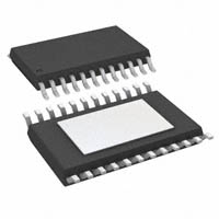
package information
TSSOP-24,
PWP Package
(TOP VIEW)
DIL-16, SOIC-16
N, DP Package
(TOP VIEW)
SHTDWN
VIN
VIN
GND*
EGND*
1
2
3
4
5
16
15
14
13
12
SHTDWN
1
24 FAULT
VIN
2
23 VOUT
VOUT
VIN
3
22 VOUT
VOUT
N/C
4
21 N/C
GND*
5
20 GND*
GND*
6
19 GND*
GND*
7
18 GND*
GND*
8
17 GND*
FAULT
GND*
GND*
B3
6
11
CT
B2
7
10
IMAX
B1
8
9
B0
EGND*
*Pin 5 serves as lowest impedance to the electrical
ground; Pins 4, 12, and 13 serve as heat sink/ground.
These pins should be connected to large etch areas to
help dissipate heat. For N Package, pins 4, 12, and 13
are N/C.
2
POST OFFICE BOX 655303
9
16 N/C
B3
10
15 CT
B2
11
14 IMAX
B1
12
13 B0
*Pin 9 serves as lowest impedance to the electrical ground;
other GND pins serve as heat sink/ground. These pins should
be connected to large etch areas to help dissipate heat.
• DALLAS, TEXAS 75265
��������� ��� ���
��
� �
��
������� ��� ���� ����
������
�
SLUS198C – FEBUARY 2000 - REVISED - JUNE 2001
electrical characteristics, these specifications apply for TA = –40°C to 85°C for the UCC2915 and
0°C to 70°C for the UCC3915, VIN = 12 V, IMAX = 0.4 V, SHTDWN = 2.4 V, TA = TJ, (unless otherwise
stated)
supply
PARAMETER
TEST CONDITIONS
Voltage input range
MIN
TYP
7.0
Supply current
Sleep mode current
SHTDWN = 0.2 V,
Output leakage
SHTDWN = 0.2 V
no load
MAX
UNITS
15.0
V
1.0
2.0
mA
100
150
µA
20
µA
NOTE 1: All voltages are with respect to GND. Current is positive into and negative out of the specified terminal.
output
PARAMETER
Voltage drop
TEST CONDITIONS
MIN
TYP
MAX
UNITS
IOUT = 1 A (10 V to 12 V)
IOUT = 2 A (10 V to 12 V)
0.15
0.3
V
0.3
0.6
V
IOUT = 3 A (10 V to 12 V)
IOUT = 1 A,
VIN = 7 V and 15 V
0.45
0.9
V
0.2
0.4
V
0.4
0.8
V
0.6
1.2
V
IOUT = 2 A,
IOUT = 3 A,
VIN = 7 V and 15 V
VIN = 7 V,
12 V MAX
Initial startup time
See Note 2
100
µs
Short circuit response
See Note 2
100
ns
Thermal shutdown
See Note 2
165
°C
Thermal hysteresis
See Note 2
10
°C
NOTE 1: All voltages are with respect to GND. Current is positive into and negative out of the specified terminal.
NOTE 2: Ensured by design. Not production tested.
DAC
PARAMETER
TEST CONDITIONS
MIN
TYP
MAX
UNITS
Code = 0000–0011 (device off)
Trip current
Tri
Code = 0100
0.07
0.25
0.45
A
Code = 0101
0.32
0.50
0.70
A
Code = 0110
0.50
0.75
0.98
A
Code = 0111
0.75
1.00
1.3
A
Code = 1000
1.0
1.25
1.6
A
Code = 1001
1.25
1.50
1.85
A
Code = 1010
1.5
1.75
2.15
A
Code = 1011
1.70
2.00
2.4
A
Code = 1100
1.90
2.25
2.7
A
Code = 1101
2.1
2.50
2.95
A
NOTE 1: All voltages are with respect to GND. Current is positive into and negative out of the specified terminal.
POST OFFICE BOX 655303
• DALLAS, TEXAS 75265
3
��������� ��� ���
��
� �
��
������� ��� ���� ����
������
�
SLUS198C – FEBUARY 2000 - REVISED - JUNE 2001
electrical characteristics, these specifications apply for TA = –40°C to 85°C for the UCC2915 and
0°C to 70°C for the UCC3915, VIN = 12 V, IMAX = 0.4 V, SHTDWN = 2.4 V, TA = TJ, (unless otherwise
stated)
DAC (continued)
PARAMETER
Trip current
c rrent
TEST CONDITIONS
MIN
TYP
MAX
UNITS
Code = 1110
2.30
2.75
3.25
A
Code = 1111
2.50
3.0
3.50
A
0.35
1.0
1.65
A
3.0
4.0
5.2
A
Max output current over trip
(current source mode)
Code = 0100 to 1111,
IMAX = 0 V
Max output current
(current source mode)
Code = 0100 to 1111,
IMAX = 2.4 V
NOTE 1: All voltages are with respect to GND. Current is positive into and negative out of the specified terminal.
fault timer
PARAMETER
CT charge current
TEST CONDITIONS
MIN
TYP
MAX
UNITS
–47
µA
1.2
1.8
µA
1.9%
3.3%
–83
CT discharge current
VCT = 1.0 V
VCT = 1.0 V
–62
0.8
Output duty cycle
VOUT = 0 V
1.0%
CT fault threshold
1.2
1.5
1.7
V
CT reset threshold
0.4
0.5
0.6
V
NOTE 1: All voltages are with respect to GND. Current is positive into and negative out of the specified terminal.
shutdown
PARAMETER
TEST CONDITIONS
Shutdown threshold
MIN
1.1
TYP
1.5
Shutdown hysteresis
150
Input current
100
MAX
1.9
UNITS
V
mV
500
nA
NOTE 1: All voltages are with respect to GND. Current is positive into and negative out of the specified terminal.
open drain output (FAULT)
PARAMETER
High level output current
TEST CONDITIONS
MIN
TYP
FAULT = 5 V
Low level output voltage
IOUT = 5 mA
NOTE 1: All voltages are with respect to GND. Current is positive into and negative out of the specified terminal.
0.2
MAX
UNITS
250
µA
0.8
V
TTL input dc characteristics
PARAMETER
TEST CONDITIONS
TTL input voltage high
MIN
TYP
TTL input low current
VIH = 2.4 V
VIL = 0.4 V
3
NOTE 1: All voltages are with respect to GND. Current is positive into and negative out of the specified terminal.
4
POST OFFICE BOX 655303
• DALLAS, TEXAS 75265
UNITS
V
TTL input voltage low
TTL input high current
MAX
2.0
0.8
V
10
µA
1
µA
��������� ��� ���
��
� �
��
������� ��� ���� ����
������
�
SLUS198C – FEBUARY 2000 - REVISED - JUNE 2001
pin descriptions
B0 – B3: These pins provide digital input to the DAC, which sets the fault-current threshold. They can be used
to provide a digital soft-start and adaptive-current limiting.
CT: A capacitor connected to ground sets the maximum-fault time. The maximum-fault time must be more than
the time required to charge the external capacitance in one cycle. The maximum-fault time is defined as
TFAULT = 16.1 × 10³ × CT. Once the fault time is reached the output will shutdown for a time given by
TSD = 833 × 103 × CT, this equates to a 1.9% duty cycle.
FAULT: Open-drain output, which pulls low upon any fault or interrupt condition, or thermal shutdown.
IMAX: When this pin is set to a logic low, the maximum-sourcing current will always be 1 A above the
programmed-fault level. When set to a logic high, the maximum-sourcing current will be a constant 4 A for
applications which require fast charging of load capacitance.
SHTDWN: When this pin is brought to a logic low, the IC is put into a sleep mode drawing typically less than
100 µA of ICC.The input threshold is hysteretic, allowing the user to program a startup delay with an external
RC circuit.
VIN: Input voltage to the UCC3915. The recommended voltage range is 7 V to 15 V. Both VIN pins should be
connected together and connected to the power source.
VOUT: Output voltage from the UCC3915. Both VOUT pins should be connected together and connected to
the load. When switched the output voltage will be approximately VIN – (0.15 Ω × IOUT). VOUT must not exceed
VIN by greater than 0.3 V.
APPLICATION INFORMATION
4
VIN
12
13
HEAT SINK
GND PINS
2
VIN
CIN
VOUT
14
VOUT
3
D1
5
GND
15
RL
COUT
UCC3915
5V
R1
S6
LED
SHTDWN
16 FAULT
11 CT
CT
B3
B2
B1
B0
IMAX
6
7
8
9
10
RSD
VIN
1
CSD
VIN
S1
S2
S3
S4
S5
DIP
SWITCH
UDG-99175
Figure 1. Evaluation Circuit
POST OFFICE BOX 655303
• DALLAS, TEXAS 75265
5
��������� ��� ���
��
� �
��
������� ��� ���� ����
������
�
SLUS198C – FEBUARY 2000 - REVISED - JUNE 2001
APPLICATION INFORMATION
protecting the UCC3915 from voltage transients
The parasitic inductance associated with the power distribution can cause a voltage spike at VIN if the load
current is suddenly interrupted by the UCC3915. It is important to limit the peak of this spike to less than 15 V
to prevent damage to the UCC3915. This voltage spike can be minimized by:
D Reducing the power distribution inductance (e.g., twist the positive (+) and negative (–) leads of the power
supply feeding VIN, locate the power supply close to the UCC3915 or use PCB power and ground planes).
D Decoupling VIN with a capacitor, CIN (refer to Figure 1), located close to the VIN pins. This capacitor is
typically 1 µF or less to limit the inrush current.
D Clamping the voltage at VIN below 15 V with a Zener diode, D1(refer to Figure 1), located close to the VIN
pins.
Figure 2. Load Current, Timing-Capacitor Voltage, and Output Voltage of the UCC3915
Under Fault Conditions
estimating maximum load capacitance
For hot-swap applications, the rate at which the total output capacitance can be charged depends on the
maximum-output current available and the nature of the load. For a constant-current, current-limited
application, the output will come up if the load asks for less than the maximum available short-circuit current.
To ensure recovery of a duty cycle from a short-circuited load condition, there is a maximum total output
capacitance which can be charged for a given unit on time (fault time). The design value of on or fault time can
be adjusted by changing the timing capacitor CT.
6
POST OFFICE BOX 655303
• DALLAS, TEXAS 75265
��������� ��� ���
��
� �
��
������� ��� ���� ����
������
�
SLUS198C – FEBUARY 2000 - REVISED - JUNE 2001
APPLICATION INFORMATION
For worst-case constant-current load of value just less than the trip limit; COUT(max) can be estimated from:
C
OUT(max)
ǒ MAX * ILOADǓ
[ I
ǒ
10 3
16.1
V
OUT
C
T
Ǔ
Where VOUT is the output voltage.
For a resistive load of value RL, the value of COUT(max) can be estimated from:
ȡ
ȣ
ȧ
ȧ
ȧ
ȧ
ȧ
ȧ
ȧ 16.1 103 C ȧ
ȧ
T ȧ
C
[
ȧ
OUT(max) ȧ
ȧ
ȱ
ȳȧ
ȧ
ȧ
ȧR ȏnȧ 1 ȧȧ
ȧL ȧ V
ȧ
ȧ
ȧ
ȧ
OUT
1
I
R
Ȳ MAX LȴȤ
Ȣ
*
Long CT times must consider the maximum temperature. Thermal shutdown protection may be the limiting fault
time.
safety recommendations
Although the UCC3915 is designed to provide system protection for all fault conditions, all integrated circuits
can ultimately fail short. For this reason, if the UCC3915 is intended for use in safety-critical applications where
UL or some other safety rating is required, a redundant safety device such as a fuse should be placed in series
with the device. The UCC3915 will prevent the fuse from blowing for virtually all fault conditions, increasing
system reliability and reducing maintenance cost, in addition to providing the hot-swap benefits of the device.
POST OFFICE BOX 655303
• DALLAS, TEXAS 75265
7
�PACKAGE OPTION ADDENDUM
www.ti.com
14-Oct-2022
PACKAGING INFORMATION
Orderable Device
Status
(1)
Package Type Package Pins Package
Drawing
Qty
Eco Plan
(2)
Lead finish/
Ball material
MSL Peak Temp
Op Temp (°C)
(3)
Device Marking
Samples
(4/5)
(6)
UCC2915DP
ACTIVE
SOIC
D
16
40
RoHS & Green
NIPDAU
Level-2-260C-1 YEAR
-40 to 85
UCC2915DP
Samples
UCC3915DP
ACTIVE
SOIC
D
16
40
RoHS & Green
NIPDAU
Level-2-260C-1 YEAR
0 to 70
UCC3915DP
Samples
UCC3915DPTR
ACTIVE
SOIC
D
16
2500
RoHS & Green
NIPDAU
Level-2-260C-1 YEAR
0 to 70
UCC3915DP
Samples
(1)
The marketing status values are defined as follows:
ACTIVE: Product device recommended for new designs.
LIFEBUY: TI has announced that the device will be discontinued, and a lifetime-buy period is in effect.
NRND: Not recommended for new designs. Device is in production to support existing customers, but TI does not recommend using this part in a new design.
PREVIEW: Device has been announced but is not in production. Samples may or may not be available.
OBSOLETE: TI has discontinued the production of the device.
(2)
RoHS: TI defines "RoHS" to mean semiconductor products that are compliant with the current EU RoHS requirements for all 10 RoHS substances, including the requirement that RoHS substance
do not exceed 0.1% by weight in homogeneous materials. Where designed to be soldered at high temperatures, "RoHS" products are suitable for use in specified lead-free processes. TI may
reference these types of products as "Pb-Free".
RoHS Exempt: TI defines "RoHS Exempt" to mean products that contain lead but are compliant with EU RoHS pursuant to a specific EU RoHS exemption.
Green: TI defines "Green" to mean the content of Chlorine (Cl) and Bromine (Br) based flame retardants meet JS709B low halogen requirements of


 工商网监
湘ICP备2023018690号
工商网监
湘ICP备2023018690号
