UCC5638
Multimode SCSI 15 Line Terminator
FEATURES
DESCRIPTION
• Auto Selection Single Ended (SE) or
Low Voltage Differential (LVD)
Termination
The UCC5638 Multimode SCSI Terminator provides a smooth transition
into the LVD SCSI Parallel Interface (SPI-2, SPI-3, SPI-4). It automatically
senses the bus, via DIFFB, and switches the termination to either single
ended (SE) or low voltage differential (LVD) SCSI, dependent on which
type of devices are connected to the bus. The UCC5638 can not be used
on a HVD, EIA485, differential SCSI bus. If the UCC5638 detects a HVD
SCSI device, it switches to a high impedance state.
• Meets SCSI-1, SCSI-2, Ultra2 (SPI-2
LVD SCSI), Ultra3, Ultra160 (SPI-3)
and Ultra320 (SPI-4) Standards
• 2.7V to 5.25V Operation
• Differential Failsafe Bias
• Thermal packaging for low junction
temperature and better MTBF.
The Multimode terminator contains all functions required to terminate and
auto detect and switch modes for SPI-2, SPI-3 and SPI-4 bus architectures.
Single Ended and Differential impedances and currents are trimmed for
maximum effectiveness. Fail Safe biasing is provided to insure signal integrity. Device/Bus type detection circuitry is integrated into the terminator to
provide automatic switching of termination between single ended and LVD
SCSI and a high impedance for HVD SCSI. The multimode function provides all the performance analog functions necessary to implement SPI-2
termination in a single monolithic device.
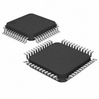
The UCC5638 is offered in a 48 pin LQFP package for a temperature range
of 0°C to 70°C.
BLOCK DIAGRAM
(NOISE LOAD)
HIGH POWER
DIFFERENTIAL
2.15V
DIFFB
REF
1.3V
LOW VOLTAGE
DIFFERENTIAL
34
0.6V
1.3V
DIFFSEN
12
L1–
11
L1+
2
L15–
1
L15+
–15mA ≤ ISOURCE ≤ –5mA
50µA ≤ ISINK ≤ 200µA
SINGLE ENDED
110
REF
2.7V
SOURCE/SINK REGULATOR
124
56mV
52.5
– +
REF
1.25V
56mV
52.5
+ –
ALL SWITCHES
MODE
UP
SE
DOWN
LVD
OPEN
DISCNCT
10µA
SE GND SWITCH
110
124
DISCNCT 36
56mV
52.5
– +
56mV
+ –
TRMPWR
35
3
52.5
SE GND SWITCH
27
HS/GND
HS/GND
4-9
28-33
10
GND
REG
4.7µF .
UDG-98063
SLUS271B - FEBRUARY 2000 - REVISED APRIL 2001
�UCC5638
ABSOLUTE MAXIMUM RATINGS
CONNECTION DIAGRAMS
TRMPWR Voltage . . . . . . . . . . . . . . . . . . . . . . . . . . . . . . . . +6V
Signal Line Voltage . . . . . . . . . . . . . . . . . . . . . . . . . . . 0V to 5V
Package Dissipation . . . . . . . . . . . . . . . . . . . . . . . . . . . . . . . 2W
Storage Temperature . . . . . . . . . . . . . . . . . . . –65°C to +150°C
Junction Temperature . . . . . . . . . . . . . . . . . . . –55°C to +150°C
Lead Temperature (Soldering, 10 sec.) . . . . . . . . . . . . . +300°C
Recommended Operating Conditions . . . . . . . . . 2.7V to 5.25V
(TOP VIEW)
FQP Package
HS/GND
HS/GND
HS/GND
HS/GND
HS/GND
HS/GND
REG
Currents are positive into negative out of the specified terminal.
Note: Consult Packaging Section of Databook for thermal limitations and considerations of package.
L1+
TRMPWR
L15–
L1–
L15+
12 11
RECOMMENDED OPERATING CONDITIONS
TRMPWR Voltage . . . . . . . . . . . . . . . . . . . . . . . . 2.7V to 5.25V
Temperature Ranges . . . . . . . . . . . . . . . . . . . . . . 0°C to +70°C
10
9
8
7
6
4
5
3
2
1
L2+
13
48
L14–
L2–
14
47
L14+
L3+
15
46
L13–
L3–
16
45
L13+
L4+
17
44
L12–
L4–
18
43
L12+
L5+
19
42
L11–
L5–
20
41
L11+
L6+
21
40
L10–
L6–
22
39
L10+
L7+
23
38
L9–
L7–
24
25 26
37
L9+
27
28
29 30
31
32
33 34
35
36
DISCNCT
L8+
L8–
GND
HS/GND
DIFFSENS
HS/GND
HS/GND
HS/GND
DIFFB
HS/GND
HS/GND
ELECTRICAL CHARACTERISTICS Unless otherwise stated, these specifications apply for TA = TJ = 0°C to 70°C,
TRMPWR = 3.3V.
PARAMETER
TEST CONDITIONS
MIN
TYP
MAX UNITS
TRMPWR Supply Current Section
TRMPWR Supply Current
LVD SCSI Mode
20
25
mA
SE SCSI Mode
1.6
10
mA
Disabled Terminator
250
400
A
V
Regulator Section
1.25V Regulator
LVD SCSI Mode
1.15
1.25
1.35
1.25V Regulator Source Current
VREG = 0V
–375
–700
–1000
mA
1.25V Regulator Sink Current
VREG = 3.3V
170
300
700
mA
1.3V Regulator
Diff Sense
1.2
1.3
1.4
V
1.3V Regulator Source Current
VREG = 0V
–15
–5
mA
1.3V Regulator Sink Current
VREG = 3.3V
50
200
A
2.7V Regulator
SE SCSI Mode
2.5
2.7
3.0
V
2.7V Regulator Source Current
VREG = 0V
–375
–700
–1000
mA
2.7V Regulator Sink Curren
VREG = 3.3V
170
300
700
mA
100
105
110
110
150
Differential Termination Section
Differential Impedance
Common Mode Impedence
(Note 2)
Differential Bias Voltage
100
Common Mode Bias
Output Capacitance
1.15
Single Ended Measurement to Ground (Note 1)
2
165
125
1.25
mV
1.35
V
3
pF
�UCC5638
ELECTRICAL CHARACTERISTICS Unless otherwise stated, these specifications apply for TA = TJ = 0°C to 70°C,
TRMPWR = 3.3V.
PARAMETER
TEST CONDITIONS
MIN
TYP
MAX UNITS
102.3
110
117.7
Signal Level 0.2V, All Lines Low
–21
–24
–25.4
mA
Signal Level 0.5V
–18
–22.4
mA
400
nA
3
pF
Single Ended Termination Section
Impedance
Z =
Termination Current
(VLX − 0 . 2V )
ILX
, (Note 3)
Output Leakage
Output Capacitance
Single Ended Measurement to Ground (Note 1)
Single Ended GND SE Impedance
I = 10mA
20
60
Disconnect and Diff Buffer Input Section
DISCNCT Threshold
0.8
2.0
V
30
A
0.5
0.7
V
Diff Buffer LVD to HPD Threshold
1.9
2.4
V
DIFFB Input Current
–10
10
A
DISCNCT Input Current
10
Diff Buffer Single Ended to LVD Threshold
Note 1: Ensured by design. Not 100% tested in production.
Note 2: Line+ (positive) tied to Line– (negative);
1. 2V
[I(VCM max) – I(VCM min)]
Note 3: VLX= Output voltage for each terminator minus output pin (L1– through L15–) with each pin unloaded.
ILX = Output current for each terminator minus output pin (L1– through L15–) with the minus output pin forced to 0.2V.
PIN DESCRIPTIONS
DIFFB: Diff sense filter pin should be connected at a
4.7 F capacitor.
LINEn–: Signal line active line for single ended or negative line in differential applications for the SCSI bus.
DIFFSENS: The SCSI bus Diff Sense line to detect what
types of devices are connected to the SCSI bus.
LINEn+: Ground line for single ended or positive line for
differential applications for the SCSI bus.
DISCNCT: Disconnect pin shuts down the terminator
when it is not at the end of the bus. The disconnect pin
low enables the terminator.
REG: Regulator bypass pin, must be connected to a
4.7 F capacitor.
TRMPWR: VIN 2.7V to 5.25V supply, bypass near the
terminator with a 4.7 F capacitor to ground.
Note: In Disconnect Mode, the comparitor set powers down for
low idle current.
3
�UCC5638
APPLICATION INFORMATION
The UCC5638 is a Multi-mode active terminator with selectable single ended (SE) and low voltage differential
(LVD) SCSI termination integrated into a monolithic component. Mode selection is accomplished with the “diff
sense" signal.
with 4 mil etch and 4 mil spacing between the runs within
a pair, and a minimum of 8 mil spacing to the next pair.
This spacing between the pairs reduces potential
crosstalk. Beware of feed-throughs and each through
hole connection adds a lot of capacitance. Standard
power and ground plane spacing yields about 1pF to
each plane. Each feed-through will add about 2.5pF to
3.5pF. Enlarging the clearance holes on both power and
ground planes can reduce the capacitance and opening
up the power and ground planes under the connector
can reduce the capacitance for through hole connector
applications. Microstrip technology is normally too low of
impedance and should not be used. It is designed for
50 rather than 120 differential systems.
The diff sense signal is a three level signal, which is
driven at each end of the bus by one active terminator.
An LVD SCSI or multi-mode terminator drives the diff
sense line to 1.3 V. If diff sense is at 1.3 V, then bus is in
LVD SCSI mode. If a single ended SCSI device is
plugged into the bus, the diff sense line is shorted to
ground. With diff sense shorted to ground, the terminator
changes to single ended mode to accommodate the SE
device. If an HVD SCSI device is plugged in to the bus,
the diff sense line is pulled high and the terminator shuts
down.
Capacitance balance is critical for Ultra2 and
Ultra3/Ultra160. The balance capacitance standard is
0.5pF per line with the balance between pairs of 2pF.
The components are designed with very tight balance,
typically 0.1pF between pins in a pair and 0.3pF between
pairs. Layout balance is critical, feed-throughs and etch
length must be balanced, preferably no feed-throughs
would be used. Capacitance for devices should be measured in the typical application, material and components
above and below the circuit board effect the capacitance.
The diff sense line is driven and monitored by the terminator through a 100ms to 300ms noise filter at the DIFFB
input pin. A set of comparators, that allow for ground
shifts, determine the bus status as follows. Any diff sense
signal below 0.5V indicates single ended, between 0.7V
and 1.9V is LVD SCSI and above 2.2V is HVD SCSI.
In the single ended mode, a multi-mode terminator has a
110 terminating resistor connected to a 2.7V termination voltage regulator. The 2.7V regulator is used on all
Unitrode terminators designed for 3.3V systems. This requires the terminator to operate in specification down to
2.7V TRMPWR voltage to allow for the 3.3V supply tolerance, an unidirectional fusing device and cable drop. At
each L+ pin, a ground driver drives the pin to ground,
while in single ended mode. The ground driver is specially designed so it will not effect the capacitive balance
of the bus when the device is in LVD SCSI or disconnect
mode. The device requirements call for 0.5pF balance on
the lines of a differential pair. The terminator capacitance
has to be a small part of the capacitance imbalance.
Multi-mode terminators need to consider power dissipation; the UCC5638 is offered in a power package with
heat sink ground pins. These heat sink/ground pins are
directly connected to the die mount paddle under the die
and conduct heat from the die to reduce the junction
temperature. These pins need to be connected to etch
area or a feed-through per pin connecting to the ground
plane layer on a multi-layer board.
In 3.3V TRMPWR systems, the UCC3912 should be
used to replace the fuse and diode. This reduces the
voltage drop, allowing for cable drop to the far end terminator. 3.3V battery systems normally have a 10% tolerance. The UCC3912 is 150mV drop under LVD SCSI
loads, allowing 150mV drop in the cable system. All Unitrode LVD SCSI and multi-mode terminators are designed for 3.3V systems, operating down to 2.7V.
Layout is very critical for Ultra2, Ultra3, Ultra160 and
Ultra320 systems. Multi-layer boards need to adhere to
the 120 impedance standard, including connector and
feed-through. This is normally done on the outer layers
4
�UCC5638
TYPICAL APPLICATION
TERMPWR
3
L1+
L1+
L1–
L1–
TRMPWR
TRMPWR
CONTROL LINES (9)
L9+
L9+
L9–
L9–
L10+
L10+
L10–
L10–
3
TRMPWR
4 BITS OF THE HIGH BYTE
L15+
L15+
L15–
L15–
36 DISCNCT
DISCNCT 36
DIFFSENSE 35
REG
DIFF B
10
34
35 DIFFSENSE
50k
4.7µF
.
DIFF B
REG
34
10
50k
4.7µF
4.7µF
4.7µF
270k
4.7µF
.
4.7µF
L1+
L1+
L1–
DATA LINES (15)
3
L1–
HIGH BYTE 4 BITS
PLUS PARITY
DATA LINES (15)
L5+
L5+
L5–
L5–
TRMPWR
TRMPWR
L6+
L6+
L6–
L6–
3
LOW BYTE 8+ PARITY
36 DISCNCT
L14+
L14+
L14–
L14–
DISCNCT 36
REG
DIFF B
DIFF B
REG
10
34
34
10
4.7µF
.
4.7µF
SCSI CONTROLLER
DIFFSENS
UDG-98064
Note: A 220k resistor is added to ground to insure the transceivers will come up in single-ended mode when no terminator is enabled. The controller DIFFSENS ties to the DIFFB pin on the terminators, only one RC network should be on a device.
5
�PACKAGE OPTION ADDENDUM
www.ti.com
10-Dec-2020
PACKAGING INFORMATION
Orderable Device
Status
(1)
Package Type Package Pins Package
Drawing
Qty
Eco Plan
(2)
Lead finish/
Ball material
MSL Peak Temp
Op Temp (°C)
Device Marking
(3)
(4/5)
(6)
UCC5638FQPTR
ACTIVE
LQFP
PT
48
1000
RoHS & Green
NIPDAU
Level-3-260C-168 HR
0 to 70
UCC5638
FQP
(1)
The marketing status values are defined as follows:
ACTIVE: Product device recommended for new designs.
LIFEBUY: TI has announced that the device will be discontinued, and a lifetime-buy period is in effect.
NRND: Not recommended for new designs. Device is in production to support existing customers, but TI does not recommend using this part in a new design.
PREVIEW: Device has been announced but is not in production. Samples may or may not be available.
OBSOLETE: TI has discontinued the production of the device.
(2)
RoHS: TI defines "RoHS" to mean semiconductor products that are compliant with the current EU RoHS requirements for all 10 RoHS substances, including the requirement that RoHS substance
do not exceed 0.1% by weight in homogeneous materials. Where designed to be soldered at high temperatures, "RoHS" products are suitable for use in specified lead-free processes. TI may
reference these types of products as "Pb-Free".
RoHS Exempt: TI defines "RoHS Exempt" to mean products that contain lead but are compliant with EU RoHS pursuant to a specific EU RoHS exemption.
Green: TI defines "Green" to mean the content of Chlorine (Cl) and Bromine (Br) based flame retardants meet JS709B low halogen requirements of


 工商网监
湘ICP备2023018690号
工商网监
湘ICP备2023018690号
