�������
SLUS314C − JANUARY 2000 − REVISED JUNE 2003
��
����
� ������������ ��
�� ���� ������ ����������
FEATURES
D First LVD only Active Terminator
D Meets SCSI SPI-2 Ultra2 (Fast-40), SPI-3 Ultra3
D
D
DESCRIPTION
The UCC5640 is an active terminator for low voltage
differential (LVD) SCSI networks. This LVD only design
allows the user to reach peak bus performance while
reducing system cost. The device is designed as an
active Y-terminator to improve the frequency response
of the LVD bus. Designed with a 1.5-pF channel
capacitance, the UCC5640 allows for minimal bus
loading for a maximum number of peripherals. With the
UCC5640, the designer will be able to comply with the
Fast-40 SPI-2, Fast-80 SPI-3 and Fast-160 SPI-4
specifications. The UCC5640 also provides a much
needed system migration path for ever improving SCSI
system standards. This device is available in the 24-pin
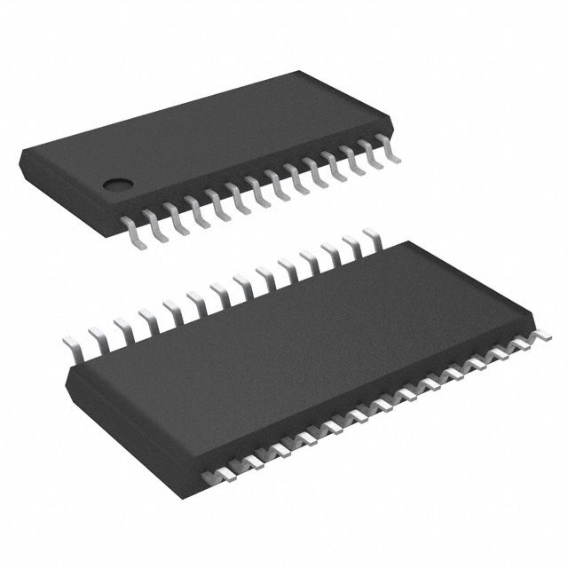
TSSOP and 28-pin TSSOP for ease of layout use.
/ Ultra160 (Fast-80) and SPI-4 (Fast-160)
Ultra320 Standards
2.7-V to 5.25-V Operation
Differential Failsafe Bias
The UCC5640 is not designed for use in single ended
(SE) or high voltage differential (HVD) systems.
BLOCK DIAGRAM
TRMPWR
28
SOURCE 5− 15mA
SINK 200 µA MAXIMUM (NOISE LOAD)
2.7V to 5.25V
REF 1.3V
OPEN CIRCUIT ON POWER OFF
OR OPEN CIRCUIT IN A
DISABLED TERMINATOR MODE
12
DIFSENS
27
LVD*
4
L1−
3
L1+
26
L9−
25
L9+
1.3V + 0.1V
HIGH POWER
DIFFERENTIAL
2.4V > 1.9V
DIFFB 11
HIGH IMPEDANCE RECEIVER
EVEN WITH POWER OFF
0.7V > 0.5V
SOURCE/SINK REGULATOR
SINGLE
ENDED
124
REF 1.25V
10 µA
124
DISCNCT
15
56mV
−
+
52
56mV
+
−
52
56mV
−
+
52
56mV
+
−
52
UDG−98181
*28 pin package only
14
1
GND
REG
These devices have limited built-in ESD protection. The leads should be shorted together or the device placed in conductive foam
during storage or handling to prevent electrostatic damage to the MOS gates.
���������� ���� �����!"#��� �$ %&��'�# "$ �� (&)*�%"#��� +"#',
���+&%#$ %�����! #� $('%���%"#���$ ('� #-' #'�!$ �� �'."$ ��$#�&!'�#$
$#"�+"�+ /"��"�#0, ���+&%#��� (��%'$$��1 +�'$ ��# �'%'$$"��*0 ��%*&+'
#'$#��1 �� "** ("�"!'#'�$,
Copyright 2003, Texas Instruments Incorporated
www.ti.com
1
��������
SLUS314C − JANUARY 2000 − REVISED JUNE 2003
ORDERING INFORMATION
PACKAGED DEVICE{
TA
TSSOP-24 (PW)
0°C to 70°C
UCC5640PW24
TSSOP-28 (PW)
UCC5640PW28
† The TSSOP packages are available taped and reeled. Add TR suffix to device type (e.g.
UCC5640PW24TR) to order quantities of 2,000 devices per reel.
CONNECTION DIAGRAM
TSSOP−24 (Top View)
PW Package
REG
L1+
L1−
1
2
3
TSSOP−28 (Top View)
PW Package
REG 1
24 TRMPWR
23 L9−
22 L9+
28 TRMPWR
N/C 2
27 LVD
L1+ 3
26 L9−
L1− 4
25 L9+
L2+ 5
24 L8−
L2− 6
23 L8+
L3+ 7
22 L7−
L2+
4
21 L8−
L2−
5
20 L8+
L3+
6
19 L7−
L3−
7
18 L7+
L3− 8
21 L7+
L4+
8
17 L6−
L4+ 9
20 L6−
L4−
9
16 L6+
L4− 10
19 L6+
15 L5−
DIFFB 11
18 L5−
DIFSENS12
17 L5+
N/C 13
16 N/C
DIFFB 10
DIFSENS 11
GND 12
14 L5+
13 DISCNCT
15 DISCNCT
GND 14
RECOMMENDED OPERATING CONDITIONS
MIN
NOM
MAX
TRMPWR voltage
2.7
5.25
Signal line voltage
0
3.6
Disconnect input voltage
0
TRMPWR
UNIT
V
°C
ABSOLUTE MAXIMUM RATINGS
over operating free-air temperature range unless otherwise noted{}
UCC5640
TRMPWR voltage
6
Signal line voltage
0 to 3.6
Package dissipation
1
Storage temperature, Tstg
−65 to 150
Operating junction temperature, TJ
–55 to 150
UNIT
V
W
°C
C
Lead temperature (soldering, 10 sec.)
300
† Stresses beyond those listed under “absolute maximum ratings” may cause permanent damage to the device. These are stress ratings only,
and functional operation of the device at these or any other conditions beyond those indicated under “recommended operating conditions” is
not implied. Exposure to absolute-maximum-rated conditions for extended periods may affect device reliability. All voltages are with respect
to GND. Currents are positive into and negative out of, the specified terminal.
‡ Currents are positive into, negative out of the specified terminal. Consult Packaging Section of Databook for thermal limitations and
considerations of packages. All voltages are referenced to GND.
2
www.ti.com
��������
SLUS314C − JANUARY 2000 − REVISED JUNE 2003
ELECTRICAL CHARACTERISTICS
TA = 0°C to 70°C, TRMPWR = 3.3 V, TA = TJ, (unless otherwise noted)
PARAMETER
TEST CONDITIONS
MIN
TYP
MAX
UNITS
TRMPWR Supply Current Section
No load
TRMPWR supply current
25
mA
400
µA
5.25
V
1.25
1.35
V
–100
–80
Disabled terminator
TRMPWR voltage
2.7
Regulator Section
1.25V regulator
DIFSENS connected to DIFFB
1.15
1.25V regulator source current
DIFSENS connected to DIFFB
1.25V regulator sink current
DIFSENS connected to DIFFB
80
100
1.3V regulator
DIFFB connected to GND
1.2
1.3
1.3V regulator source current
DIFSENS to GND
1.3V sink current
DIFSENS to 3.3 V
Differential impedance
–2.5 mA to 4.5 mA
100
105
110
Common mode impedance
L+ connected to L–
110
150
165
Differential bias voltage
No load, L+ or L–
125
mV
1.25
1.35
V
10
400
nA
3
pF
mA
1.4
V
–15
–5
mA
50
200
µA
Differential Termination Section
100
Common mode bias
1.15
Output leakage, disconnect
DISCNCT, TRMPWR = 0 V to 5.25 V,
VLINE = 0.2 V to 5.25 V
Output capacitance
Single ended measurement to ground (1)
Ω
Low Voltage Differential (LVD) Status Bit Section
ISOURCE
ISINK
VLOAD = 2.4 V
–6
VLOAD = 0.4 V
2
–4
mA
5
Disconnect & Differential Sense Input Section
DISCNCT threshold
0.8
Input current
At 0 V and 3.3 V
–30
2
Differential sense SE to LVD threshold
0.5
0.7
Differential sense LVD to HPD threshold
1.9
2.4
NOTE:
V
µA
–10
V
(1) Ensured by design. Not production tested.
TERMINAL FUNCTIONS
TERMINAL(1)
NAME
NO.
I/O
DESCRIPTION
10
Differential sense filter pin should be connected to a 4.7-µF capacitor and 50-kΩ resistor to diff
sense.
DIFSENS
11
The SCSI bus differential sense line to detect what type of devices are connected to the SCSI bus.
DISCNCT
13
Disconnect pin shuts down the terminator when it is not at the end of the bus.
GND
12
DIFFB
I
Ground reference for the device.
Ln−
I
Negative line in differential applications for the SCSI bus.
Ln+
I
Positive line in differential applications for the SCSI bus.
LVD
REG
TRMPWR
NOTE:
I
Indicates that the bus is in LVD mode (28-pin package only).
1
I
Regulator bypass; must be connected to a 4.7-µF capacitor to ground.
24
I
VIN 2.7-V to 5.25-V power supply.
(1) 24-pin package.
www.ti.com
3
��������
SLUS314C − JANUARY 2000 − REVISED JUNE 2003
APPLICATION INFORMATION
All SCSI buses require a termination network at each end to function properly. Specific termination requirements
differ, depending on which types of SCSI driver devices are present on the bus. The UCC5640 is a low-voltage
differential only device. It senses which types of drivers are present on the bus. If it detects the presence of a
single-ended or high-voltage differential driver, the UCC5640 will place itself in a high-impedance input state,
effectively disconnecting the chip from the bus.
The UCC5640 senses what drivers are present on the bus by the voltage on SCSI bus control line DIFFSENS,
which is monitored by the DIFFB input pin. The DIFSENS output pin on the UCC5640 attempts to drive a
DIFFSENS control line to 1.3 V. If only LVD devices are present, the DIFFSENS line will be successfully driven
to that voltage. If HVD drivers are present, they will pull the DIFFSENS line high. If any single-ended drivers
are present, they pull the DIFSENS line to ground (even if HVD drivers are also present on the bus). If the voltage
on the DIFFB is below 0.5 V or above 2.4 V, the UCC5640 enters the high-impedance SE/HVD state. If it is
between 0.7 V and 1.9 V, the UCC5640 enters the LVD mode. These thresholds accommodate differences in
ground potential that can occur between the ends of long bus lines.
Three UCC5640 devices are required at each end of the SCSI bus to terminate 27 lines (18 data, 9 control).
Every UCC5640 contains a DIFSENS driver, but only one should be used to drive the line at each end. The
DIFSENS pin on the other devices should be left unconnected.
On power up, the voltage on the TRMPWR pin rising above 2.7 V, the UCC5640 assumes the SE/HVD mode.
The DIFFB inputs on all three chips at each end of the bus should be connected together. Properly filtered, noise
on DIFFB will not cause a false mode change. There should be a shared 50-Hz noise filter implemented on
DIFFB at each end of the bus as close as possible to the DIFFB pins. This is implemented with a 50-kΩ resistor
between the DIFFB and DIFSENS pins, and a 4.7-µF capacitor from DIFFB to ground. See Figure 1, the typical
application diagram on page 6.
In LVD mode, the regulated voltage is switched to 1.25 V and a resistor network is presented to each line pair
that provides common-mode impedance of 150 Ω and differential impedance of 105 Ω. The lines in each
differential pair are biased so that when not driven, Line(n)+ and Line(n)− are driven 56 mV below and above
the common-mode bias voltage of 1.25 V respectively.
In SE/HVD mode, all the terminating resistors are switched off the bus. The 1.25 V and 1.3 V (DIFSENS)
regulators are left on.
When the disconnect input (DISCNCT) is active (high), the terminating resistors are switched off the bus and
both voltage regulators are turned off to save power. The mode change filter/delay function is still active and
the LVD pin in the 28-pin package continues to indicate the correct bus mode.
4
www.ti.com
��������
SLUS314C − JANUARY 2000 − REVISED JUNE 2003
APPLICATION INFORMATION
The UCC5640 operates down to a TRMPWR voltage of 2.7 V. This accommodates a 3.3-V system with
allowance for supply tolerance of +10%, a unidirectional fusing device and cable drop. The UCC3912 or
UCC3918 is recommended on a 3.3-V systems and the UCC3916 is recommended on 5-V systems in place
of a fuse and diode implementation, as its lower voltage drop provides additional voltage margin for the system.
Layout is important in all SCSI implementations and critical in SPI-3 and SPI-4 systems, which have stringent
requirements on both the absolute value of capacitance on differential signal lines and the balancing of
capacitance between paired lines and from pair-to-pair.
Feedthroughs, through-hole connections, and etch lengths need to be carefully balanced. Standard multilayer
power and ground plane spacing adds about 1 pF to each plane. Each feed-through will add 2.5 pF to 3.5 pF.
Enlarging the clearance holes on both power and ground planes reduces capacitance. Opening up the power
and ground planes under a through-hole connector reduces added capacitance in those applications.
Capacitance is also affected by components in close proximity on both sides of the board.
Table 1. Maximum Capacitance
SCSI CLASS
TRACE TO GND:
REQ, ACK, DATA,
PARITY, P_CRCA
TRACE TO TRACE:
REQ, ACK, DATA,
PARITY, P_CRCAALS
TRACE TO GND:
OTHER SIGNALS
TRACE TO TRACE:
OTHER SIGNALS
Ultra1
25 pF
N/A
25 pF
N/A
13 pF
Ultra2
20 pF
10 pF
25 pF
Ultra3/Ultra160
15 pF
8 pF
25 pF
13 pF
Ultra320
13 pF
6.5 pF
21 pF (est.)
10 pF (est.)
TI terminators are designed with very tightly controlled capacitance on their signal lines. Between the positive
and negative lines in a differential pair the difference is typically no more than 0.1 pF, and only 0.3 pF between
pairs.
Multilayer boards need to adhere to the 120-Ω impedance standard, including the connector and feedthroughs.
Bus traces are normally run on the outer layers of the board with 4-mil etch and 4-mil spacing between the two
lines in each differential pair, and a minimum of 8-mil spacing to adjacent pairs to minimize crosstalk. Microstrip
technology is too low in impedance and should not be used, they are designed for 50-Ω rather than 120-Ω
differential systems.
Decoupling capacitors should be installed as close as possible to the following input pins of the UCC5640:
1. TRMPWR: 4.7-µF capacitor to ground, 0.01-µF capacitor to ground (high frequency, low ESR)
2. REG: 4.7-µF capacitor to ground, 0.01-µF capacitor to ground (high frequency, low ESR)
www.ti.com
5
��������
SLUS314C − JANUARY 2000 − REVISED JUNE 2003
APPLICATION INFORMATION
UCC5640PW28
Termpower
28
TRMPWR
27
LVD
15
DISCNCT
UCC5640PW24
L1+
3
L1−
4
2
L1+
3
L1−
Termpower
CONTROL LINES (9)
L9+
25
22
L9+
L9−
26
23
L9−
REG
DIFFB
1
11
4.7µF
DIFF SENSE
12
50k
11
50k
DISCNCT 13
DIFFB
REG
10
1
4.7µF
TRMPWR
4.7µF
4.7µF
UCC5640PW28
28
TRMPWR 24
UCC5640PW24
L1+
3
2
L1+
L1−
4
3
L1−
TRMPWR 24
DATA LINES (9)
4.7µF
15
DISCNCT
L9+
25
22
L9+
L9−
26
23
L9−
NC
12
11
NC
REG
DIFFB
DIFFB
REG
1
11
10
1
4.7µF
4.7µF
UCC5640PW28
28
TRMPWR
4.7µF
DISCNCT 13
UCC5640PW24
L1+
3
2
L1+
L1−
4
3
L1−
TRMPWR 24
DATA LINES (9)
15
S1*
DISCNCT
L9+
25
22
L9+
L9−
26
23
L9−
NC
12
11
NC
REG
DIFFB
DIFFB
REG
1
11
10
1
S2*
4.7µF
4.7µF
UDG−98100
* CLOSE S1 AND S2 TO CONNECT TERMINATORS
Figure 1. Application Diagram
6
DISCNCT 13
www.ti.com
�PACKAGE OPTION ADDENDUM
www.ti.com
10-Dec-2020
PACKAGING INFORMATION
Orderable Device
Status
(1)
Package Type Package Pins Package
Drawing
Qty
Eco Plan
(2)
Lead finish/
Ball material
MSL Peak Temp
Op Temp (°C)
(3)
Device Marking
(4/5)
(6)
UCC5640PW24TR
ACTIVE
TSSOP
PW
24
2000
RoHS & Green
NIPDAU
Level-1-260C-UNLIM
0 to 70
UCC5640PW
-24
(1)
The marketing status values are defined as follows:
ACTIVE: Product device recommended for new designs.
LIFEBUY: TI has announced that the device will be discontinued, and a lifetime-buy period is in effect.
NRND: Not recommended for new designs. Device is in production to support existing customers, but TI does not recommend using this part in a new design.
PREVIEW: Device has been announced but is not in production. Samples may or may not be available.
OBSOLETE: TI has discontinued the production of the device.
(2)
RoHS: TI defines "RoHS" to mean semiconductor products that are compliant with the current EU RoHS requirements for all 10 RoHS substances, including the requirement that RoHS substance
do not exceed 0.1% by weight in homogeneous materials. Where designed to be soldered at high temperatures, "RoHS" products are suitable for use in specified lead-free processes. TI may
reference these types of products as "Pb-Free".
RoHS Exempt: TI defines "RoHS Exempt" to mean products that contain lead but are compliant with EU RoHS pursuant to a specific EU RoHS exemption.
Green: TI defines "Green" to mean the content of Chlorine (Cl) and Bromine (Br) based flame retardants meet JS709B low halogen requirements of


 工商网监
湘ICP备2023018690号
工商网监
湘ICP备2023018690号
