VCA2618
VCA 261 8
SBOS254B – JULY 2002 – REVISED NOVEMBER 2003
Dual, VARIABLE GAIN AMPLIFIER with Input Buffer
FEATURES
GAIN RANGE: up to 43dB 30MHz BANDWIDTH LOW CROSSTALK: 65dB at Max Gain, 5MHz HIGH-SPEED VARIABLE GAIN ADJUST POWER SHUTDOWN MODE HIGH IMPEDANCE INPUT BUFFER
DESCRIPTION
The VCA2618 is a highly integrated, dual receive channel, Variable Gain Amplifier (VGA) with analog gain control. The VCA2618’s VGA section consists of two parts: the Voltage Controlled Attenuator (VCA) and the Programmable Gain Amplifier (PGA). The gain and gain range of the PGA can be digitally programmed. The combination of these two programmable elements results in a variable gain ranging from 0dB up to a maximum gain as defined by the user through external connections. The single-ended unity gain input buffer provides predictable high input impedance. The output of the VGA can be used in either a single-ended or differential mode to drive high-performance Analog-to-Digital (A/D) converters. A separate power-down pin reduces power consumption. The VCA2618 also features low crosstalk and outstanding distortion performance. The combination of low noise and gain range programmability make the VCA2618 a versatile building block in a number of applications where noise performance is critical. The VCA2618 is available in a TQFP-32 package.
CP2A CP1A
APPLICATIONS
ULTRASOUND SYSTEMS WIRELESS RECEIVERS TEST EQUIPMENT RADAR
VCA2618 (1 of 2 Channels) NOUTA Voltage Control Attenuator Programmable Gain Amplifier
INA
Buffer
POUTA
MGS1 VCACNTL Analog Control Maximum Gain Select MGS2 MGS3
Maximum Gain Select
NOUTB Voltage Control Attenuator Programmable Gain Amplifier
INB
Buffer
POUTB
CP2B
CP1B
Please be aware that an important notice concerning availability, standard warranty, and use in critical applications of Texas Instruments semiconductor products and disclaimers thereto appears at the end of this data sheet. All trademarks are the property of their respective owners.
PRODUCTION DATA information is current as of publication date. Products conform to specifications per the terms of Texas Instruments standard warranty. Production processing does not necessarily include testing of all parameters.
Copyright © 2002–2003, Texas Instruments Incorporated
www.ti.com
�ABSOLUTE MAXIMUM RATINGS(1)
Power Supply (+VS) ............................................................................. +6V Analog Input ............................................................. –0.3V to (+VS + 0.3V) Logic Input ............................................................... –0.3V to (+VS + 0.3V) Case Temperature ......................................................................... +100°C Junction Temperature .................................................................... +150°C Storage Temperature ...................................................... –40°C to +150°C NOTE: (1) Stresses above those listed under “Absolute Maximum Ratings” may cause permanent damage to the device. Exposure to absolute maximum conditions for extended periods may affect device reliability.
ELECTROSTATIC DISCHARGE SENSITIVITY
This integrated circuit can be damaged by ESD. Texas Instruments recommends that all integrated circuits be handled with appropriate precautions. Failure to observe proper handling and installation procedures can cause damage. ESD damage can range from subtle performance degradation to complete device failure. Precision integrated circuits may be more susceptible to damage because very small parametric changes could cause the device not to meet its published specifications.
PACKAGE/ORDERING INFORMATION
PACKAGE DESIGNATOR(1) PBS SPECIFIED TEMPERATURE RANGE –40°C to +85°C PACKAGE MARKING VCA2618Y ORDERING NUMBER VCA2618YT VCA2618YR TRANSPORT MEDIA, QUANTITY Tape and Reel, 250 Tape and Reel, 2000
PRODUCT VCA2618Y
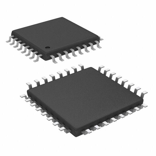
PACKAGE-LEAD TQFP-32 Surface-Mount
"
"
"
"
"
NOTE: (1) For the most current specifications and package information, refer to our web site at www.ti.com.
ELECTRICAL CHARACTERISTICS
At TA = +25°C, VDD = 5V, load resistance = 500Ω on each output to ground differential output (2VPP), MGS = 111, and fIN = 5MHz, unless otherwise noted. VCA2618Y PARAMETER BUFFER Input Resistance Input Capacitance Input Bias Current Maximum Input Voltage Input Voltage Noise Input Current Noise Noise Figure Bandwidth CONDITIONS MIN TYP MAX UNITS kΩ pF nA VPP nV/Hz fA/Hz dB MHz VPP MHz V/µs V Ω mA dBc dBc dBc dB ns dBc dB ns dB/V dB dB mV V MΩ µs 5.25 150 V mW mW
PGA Gain = 45dB, RS = 50Ω Independent of Gain RF = 550Ω, PGA Gain = 45dB, RS = 75Ω
600 5 1 1 5.4 350 13 100 1 30 300 2.5 ±1 1 ±40 –50 –50 –60 –40 to –45 5 –59 65 13 16 ±2.0 ±1.3 ±50 0.2 to 3.0 1 0.2 4.75 5.0 120 9.2
PROGRAMMABLE VARIABLE GAIN AMPLIFIER Peak Input Voltage –3dB Bandwidth Slew Rate Output Signal Range RL > 500Ω Each Side to Ground Output Impedance Output Short-Circuit Current 3rd-Harmonic Distortion VOUT = 2VPP, VCACNTL = 3.0V 2nd-Harmonic Distortion VOUT = 2VPP, VCACNTL = 3.0V VOUT = 2VPP, VCACNTL = 3.0V, MGS = 011 2nd-Harmonic Distortion Overload Performance (2nd-Harmonic Input Signal = 1VPP, VCACNTL = 2V Distortion) Time Delay IMD, 2-Tone VOUT = 2VPP, f = 9.95MHz Crosstalk Group Delay Variation 1MHz < f < 10MHz, Full Gain Range ACCURACY Gain Slope Gain Error(1) Output Offset Voltage GAIN CONTROL INTERFACE Input Voltage (VCACNTL) Range Input Resistance Response Time POWER SUPPLY Specified Operating Range Power Dissipation Power-Down NOTE: (1) Referenced to best fit dB-linear curve. VCACNTL = 0.2V to 3.0V VCACNTL = 0.2V to 3.0V VCACNTL = 0.4V to 2.9V
–45 –42
±2
45dB Gain Change
Operating, Each Channel
2
VCA2618
www.ti.com
SBOS254B
�PIN CONFIGURATION
Top View NOUTA GNDA POUTA TQFP
32
31
30
29
28
VDDA
DNC
CP2A
CP1A
NC
27
26
+INA NC VDDR VBIAS VCM GNDR NC +INB
1 2 3 4 VCA2618 5 6 7 8
25
24 23 22 21 20 19 18 17
VCACNTL MGS3 MGS2 MGS1 PD NC NC DNC
10
11
12
13
14
15 POUTB
PIN DESCRIPTIONS
PIN 1 2 3 4 5 6 7 8 9 10 11 12 13 14 15 16 DESIGNATOR +INA NC VDDR VBIAS VCM GNDR NC +INB NC DNC CP2B CP1B VDDB GNDB POUTB NOUTB DESCRIPTION Noninverting Input Channel A No Internal Connection Internal Reference Supply Bias Voltage Common-Mode Voltage Internal Reference Ground Not Connected Noninverting Input Channel B No Internal Connection Do Not Connect Coupling Capacitor Channel B Coupling Capacitor Channel B +5V Supply Channel B Ground Channel B Positive Output Channel B Negative Output Channel B PIN 17 18 19 20 21 22 23 24 25 26 27 28 29 30 31 32 DESIGNATOR DNC NC NC PD MGS1 MGS2 MGS3 VCACNTL NOUTA POUTA GNDA VDDA CP1A CP2A DNC NC DESCRIPTION Do Not Connect No Internal Connection No Internal Connection Power-Down (Active LOW) Maximum Gain Select 1 (MSB) Maximum Gain Select 2 Maximum Gain Select 3 (LSB) VCA Analog Control Negative VCA Output Channel A Positive VCA Output Channel A Ground Channel A +5V Supply Channel A Coupling Capacitor Channel A Coupling Capacitor Channel A Do Not Connect No Internal Connection
VCA2618
SBOS254B
NOUTB
VDDB
CP2B
CP1B
GNDB
NC
DNC
16
9
www.ti.com
3
�TYPICAL CHARACTERISTICS
At TA = +25°C, VDD = 5V, load resistance = 500Ω on each output to ground, differential output (2VPP) MGS = 111, and fIN = 5MHz, unless otherwise noted.
GAIN vs VCA 50 45 40 35 30 25 20 15 10 5 0 –5 0.2 0.4 0.6 0.8 1.0 1.2 1.4 1.6 1.8 2.0 2.2 2.4 2.6 2.8 3.0 VCACNTL (V) MGS = 001 MGS = 010 MGS = 011 MGS = 111 MGS = 110 MGS = 101 MGS = 100 2.0 1.5
GAIN ERROR vs TEMPERATURE +85°C +25°C 1.0
Gain Error (dB)
Gain (dB)
0.5 0 –0.5 –1.0 –1.5 –2.0 0.2 0.4 0.6 0.8 1.0 1.2 1.4 1.6 1.8 2.0 2.2 2.4 2.6 2.8 3.0 VCACNTL (V) –40°C
GAIN ERROR vs VCACNTL 2.5 2.0 1.5 10MHz 2.5 2.0 1.5
GAIN ERROR vs VCACNTL MGS = 001 MGS = 011
Gain Error (dB)
0.5 0 –0.5 –1.0 –1.5 –2.0 –2.5 0.2 0.4 0.6 0.8 1.0 1.2 1.4 1.6 1.8 2.0 2.2 2.4 2.6 2.8 3.0 VCACNTL (V) 5MHz 1MHz
Gain Error (dB)
1.0
1.0 0.5 0 –0.5 –1.0 –1.5 –2.0 –2.5 0.2 0.4 0.6 0.8 1.0 1.2 1.4 1.6 1.8 2.0 2.2 2.4 2.6 2.8 3.0 VCACNTL (V) MGS = 111
GAIN MATCH: CHA to CHB, VCACNTL = 0.2V 50 45 40 35 30
45 40 35 30
GAIN MATCH: CHA to CHB, VCACNTL = 3.0V
Units
25 20 15 10 5 0
Units –0.36 –0.30 –0.24 –0.18 –0.12 –0.06 0 0.06 0.12 0.18 0.24 0.30 0.36 0.42 0.48 0.54 0.60 0.66 0.72 0.78 0.84 0.90
25 20 15 10 5 0
Delta Gain (dB)
4
www.ti.com
–0.07 –0.06 –0.05 –0.04 –0.03 –0.02 –0.01 0 0.01 0.02 0.03 0.04 0.05 0.06 0.07 0.08 0.09 0.10 0.11 0.12 0.13 0.14 0.15 0.16 0.17 0.18
Delta Gain (dB)
VCA2618
SBOS254B
�TYPICAL CHARACTERISTICS (Cont.)
At TA = +25°C, VDD = 5V, load resistance = 500Ω on each output to ground, differential output (2VPP) MGS = 111, and fIN = 5MHz, unless otherwise noted.
GAIN vs FREQUENCY (VCACNTL = 3.0V) 50 45 40 35
Gain (dB) 40
GAIN vs FREQUENCY
MGS = 111
50
VCACNTL = 3.0V
MGS = 011
30
25 20 15 10 5 0 100k 1M Frequency (Hz) 10M 100M MGS = 001
Gain (dB)
30
20 VCACNTL = 1.6V 10 0 VCACNTL = 0.2V –10 100k 1M Frequency (Hz) 10M 100M
OUTPUT REFERRED NOISE vs VCACNTL 500 450 400 RS= 50Ω MGS = 111 600 550 500 450 400 350 300 250 200 150 100 50 0
INPUT REFERRED NOISE vs VCACNTL RS= 50Ω
Noise (nV/√Hz)
300 250 200 150 100 50 0 0.2 0.4 0.6 0.8 1.0 1.2 1.4 1.6 1.8 2.0 2.2 2.4 2.6 2.8 3.0 VCACNTL (V) MGS = 011
Noise (nV/√Hz)
350
MGS = 111
MGS = 011 0.2 0.4 0.6 0.8 1.0 1.2 1.4 1.6 1.8 2.0 2.2 2.4 2.6 2.8 3.0 VCACNTL (V)
100
INPUT REFERRED NOISE vs RS
NOISE FIGURE vs RS 24 22 20 Noise Figure (dB) 18 16 14 12 10 8 6 4 2
Noise (nV√Hz)
10
1 1 10 RS (Ω) 100 1k
10
100 RS (Ω)
1k
VCA2618
SBOS254B
www.ti.com
5
�TYPICAL CHARACTERISTICS (Cont.)
At TA = +25°C, VDD = 5V, load resistance = 500Ω on each output to ground, differential output (2VPP) MGS = 111, and fIN = 5MHz, unless otherwise noted.
60 55 50 45 40 35 30 25 20 15 10 5 0
NOISE FIGURE vs VCACNTL
HARMONIC DISTORTION vs FREQUENCY (Differential, 2Vp-p, MGS = 001) –30 –35
Harmonic Distortion (dBc)
VCACNTL = 0.2V, H2 VCACNTL = 0.2V, H3 VCACNTL = 3.0V, H2 VCACNTL = 3.0V, H3
–40 –45 –50 –55 –60 –65 –70 100k
Noise Figure (dB)
0.2 0.4 0.6 0.8 1.0 1.2 1.4 1.6 1.8 2.0 2.2 2.4 2.6 2.8 3.0 VCACNTL (V)
1M Frequency (Hz)
10M
HARMONIC DISTORTION vs FREQUENCY (Differential, 2Vp-p, MGS = 011) –30 –35 –40 –45 –50 –55 –60 –65 –70 –75 –80 –85 –90 100k
–30 –35
Harmonic Distortion (dBc)
HARMONIC DISTORTION vs FREQUENCY (Differential, 2Vp-p, MGS = 111)
VCACNTL = 0.2V, H2 VCACNTL = 0.2V, H3 VCACNTL = 3.0V, H2 VCACNTL = 3.0V, H3
Harmonic Distortion (dBc)
–40 –45 –50 –55 –60 –65 –70 –75
VCACNTL = 0.2V, H2 VCACNTL = 0.2V, H3 VCACNTL = 3.0V, H2 VCACNTL = 3.0V, H3 1M Frequency (Hz) 10M
–80 100k
1M Frequency (MHz)
10M
HARMONIC DISTORTION vs FREQUENCY (Single-Ended, 1Vp-p, MGS = 001) –30 –35
Harmonic Distortion (dBc) Harmonic Distortion (dBc)
HARMONIC DISTORTION vs FREQUENCY (Single-Ended, 1Vp-p, MGS = 011) –30 –35 –40 –45 –50 –55 –60 –65 –70 –75 –80 –85 –90 100k
VCACNTL = 0.2V, H2 VCACNTL = 0.2V, H3 VCACNTL = 3.0V, H2 VCACNTL = 3.0V, H3
–40 –45 –50 –55 –60 –65 –70 –75 –80 –85 –90 100k VCACNTL = 0.2V, H2 VCACNTL = 0.2V, H3 VCACNTL = 3.0V, H2 VCACNTL = 3.0V, H3 1M Frequency (Hz) 10M
1M Frequency (Hz)
10M
6
VCA2618
www.ti.com
SBOS254B
�TYPICAL CHARACTERISTICS (Cont.)
At TA = +25°C, VDD = 5V, load resistance = 500Ω on each output to ground, differential output (2VPP) MGS = 111, and fIN = 5MHz, unless otherwise noted.
HARMONIC DISTORTION vs FREQUENCY (Single-Ended, 1Vp-p, MGS = 111) –30 –35
Harmonic Distortion (dBc)
Harmonic Distortion (dBc) 0 –5 –10 –15 –20 –25 –30 –35 –40 –45 –50 –55 –60 –65 –70 –75 –80
HARMONIC DISTORTION vs VCACNTL (Differential, 2Vp-p) MGS = 001, H2 MGS = 011, H2 MGS = 111, H2 MGS = 001, H3 MGS = 011, H3 MGS = 111, H3
–40 –45 –50 –55 –60 –65 –70 –75 –80 –85 –90 100k 1M Frequency (Hz)
VCACNTL = 0.2V, H2 VCACNTL = 0.2V, H3 VCACNTL = 3.0V, H2 VCACNTL = 3.0V, H3
10M
0.2 0.4 0.6 0.8 1.0 1.2 1.4 1.6 1.8 2.0 2.2 2.4 2.6 2.8 3.0 VCACNTL (V)
HARMONIC DISTORTION vs VCACNTL (Single-Ended, 1Vp-p) 0 –5 –10 –15 –20 –25 –30 –35 –40 –45 –50 –55 –60 –65 –70 –75 VCACNTL (V)
0
INTERMODULATION DISTORTION (Single-Ended, 1Vp-p, fIN = 10MHz, VCACNTL = 3.0V) –10 –20
Harmonic Distortion (dBc)
Amplitude (dB)
MGS = 001, H2 MGS = 011, H2 MGS = 111, H2 MGS = 001, H3 MGS = 011, H3 MGS = 111, H3
–30 –40 –50 –60 –70 –80 –90 –100
0.2 0.4 0.6 0.8 1.0 1.2 1.4 1.6 1.8 2.0 2.2 2.4 2.6 2.8 3.0
9.5
9.6
9.7
9.8
9.9 10.0 10.1 10.2 10.3 10.4 10.5 Frequency (MHz)
0 –10 –20
INTERMODULATION DISTORTION (Differential, 2Vp-p, fIN = 10MHz, VCACNTL = 3.0V)
0 –10 –20 Cross Talk (dB) –30 –40 –50 –60 –70 –80 –90
CROSS TALK vs FREQUENCY (Differential, 2Vp-p, MGS = 011)
VCACNTRL = 0V
Amplitude (dB)
–30 –40 –50 –60 –70 –80 –90 –100 9.5 9.6 9.7 9.8 9.9 10 10.1 10.2 10.3 10.4 10.5 Frequency (MHz)
VCACNTRL = 1.5V
VCACNTRL = 3.0V
1
6
11 Frequency (MHz)
16
21
VCA2618
SBOS254B
www.ti.com
7
�TYPICAL CHARACTERISTICS (Cont.)
At TA = +25°C, VDD = 5V, load resistance = 500Ω on each output to ground, differential output (2Vp-p) MGS = 111, and fIN = 5MHz, unless otherwise noted.
OVERLOAD DISTORTION vs FREQUENCY 0
2nd-Harmonic Distortion (dBc)
–10 –20
0.1V 0.25V 0.5V 1V
59 57 55
ICC vs TEMPERATURE
ICC (mA)
53 51 49 47 45
–30 –40 –50 –60 1M Frequency (Hz) 10M
–40
–25
–10
5
20
35
50
65
80
95
Temperature (°C)
GROUP DELAY (1MHz Aperture) 15 14 13 12 11 10 9 8 7 6 5 4 3 2 1 0 1M
Group Delay (ns)
VCACNTL = 3.0V
VCACNTL = 0.2V
10M Frequency (Hz)
100M
8
VCA2618
www.ti.com
SBOS254B
�OVERVIEW
The VCA2618 is a dual-channel, VGA consisting of three primary blocks, an Input Buffer, a VCA, and a PGA. All stages are AC coupled, with the coupling into the PGA stage being made variable by placing an external capacitor between the CP1 and CP2 pins. This will be discussed further in the PGA section. By using the internal coupling into the PGA, the result is a high-pass filter characteristic with cutoff at approximately 75kHz. The output PGA naturally rolls off at around 30MHz, making the usable bandwidth of the VCA2618 between 75kHz and 30MHz.
power-on time of the VCA2618 would be increased. If a decrease in the power-on time is needed, the value can be decreased to no less than 100pF.
VOLTAGE-CONTROLLED ATTENUATOR
The magnitude of the VCA input signal from the input buffer is reduced by a programmable attenuation factor, set by the analog VCA Control Voltage (VCACNTL) at pin 24. The maximum attenuation is programmable by using the three MGS bits (pins 21, 22, and 23). Figure 2 illustrates this dual-adjust characteristic.
0
Buffer
VCA
PGA
VCA Attenuation (dB)
Channel A Input
Channel A Output
Minimum Attenuation
VCA Control
Analog Control
Maximum Gain Select
–25
MGS
Channel B Input
Buffer
VCA
PGA
Channel B Output
–43 0
Maximum Attenuation
3.0V
Control Voltage
FIGURE 1. Simplified Block Diagram of the VCA2618.
FIGURE 2. Swept Attenuator Characteristic. The MGS bits adjust the overall range of attenuation and maximum gain while the VCACNTL voltage adjusts the actual attenuation factor. At any given maximum gain setting, the analog variable gain characteristic is linear in dB as a function of the control voltage, and is created as a piecewise approximation of an ideal dB-linear transfer function. The VCA control circuitry is common to both channels of the VCA2618. The range for the VCACNTL input spans from 0V to 3V. Although overdriving the VCACNTL input above the recommended 3V maximum will not damage the part, this condition should be avoided.
INPUT BUFFER
The input buffer is a unity gain amplifier (gain of +1) with a bandwidth of 100MHz with an input resistance of approximately 600kΩ. The input buffer isolates the circuit driving the VCA2618 inputs from the internal VCA block, which would present a varying impedance to the input circuitry. To allow symmetrical operation of the input buffer, the input to the buffer must be AC coupled through an external capacitor. The recommended value of the capacitor is 0.01µF. It should be noted that if the capacitor value were increased, the
RS Input Q1A VCM Q1B Q2A Q2B Q3A Q3B Q4A Q4B Q5A Q5B Output
A1 B1 B2
A2
A3
A4
A5
FIGURE 3. Programmable Attenuator Section.
VCA2618
SBOS254B
www.ti.com
9
�Attenuator Input RS
A1 to A10 Attenuator Stages QS
Attenuator Output
Q1 VCM A1 C1 A2 C2
Q2 A3 C3
Q3 A4 C4
Q4 A5 C5
Q5 A6 C6
Q6 A7 C7
Q7 A8 C8
Q8 A9 C9
Q9 A10
Q10
C10
V1
V2
V3
V4
V5
V6
V7
V8
V9
V10
Control Input
C1 to C10 Clipping Amplifiers
0dB
–4.3dB Attenuation Characteristic of Individual FETs
VCM – VT
0 V1 V2 V3 V4 V5 V6 V7 V8 V9 V10
Characteristic of Attenuator Control Stage Output
OVERALL CONTROL CHARACTERISTICS OF ATTENUATOR 0dB
–43dB 0.3V Control Signal 3V
FIGURE 4. Piecewise Approximation to Logarithmic Control Characteristics.
10
VCA2618
www.ti.com
SBOS254B
�PGA POST-AMPLIFIER
Figure 5 shows a simplified circuit diagram of the PGA block. As stated before, the input to the PGA is AC coupled by an internal capacitor. Provisions are made so that an external capacitor can be placed in parallel with the internal capacitor, thus lowering the usable low-frequency bandwidth. The lowfrequency bandwidth is set by the following equation:
MGS SETTING 000 001 010 011 100 101 110 111
ATTENUATOR GAIN VCACNTL = 0V to 3V Not Valid –25dB to 0dB –28dB to 0dB –31dB to 0dB –34dB to 0dB –37dB to 0dB –40dB to 0dB –43dB to 0dB
ATTENUATOR + DIFFERENTIAL PGA GAIN Not Valid 0dB to 25dB 0dB to 28dB 0dB to 31dB 0dB to 34dB 0dB to 37dB 0dB to 40dB 0dB to 43dB
(
1 2 • π • 500k Ω • (220pF + CEXTERNAL )
)
where CEXTERNAL is the external capacitor value in farads. Care should be taken to avoid using too large a value of capacitor, as this can increase the power-on delay time. As described previously, the PGA gain is programmed with the same MGS bits that control the VCA maximum attenuation factor. Specifically, the maximum PGA gain at each MGS setting is the inverse (reciprocal) of the maximum VCA attenuation at that setting. Therefore, the VCA + PGA overall gain will always be 0dB (unity) when the analog VCACNTL input is set to 0V (the maximum attenuation for VCA). For VCACNTL = 3V (no attenuation), the VCA + PGA gain will be controlled by the programmed PGA gain (25dB to 43dB in 3dB steps). For clarity, the gain and attenuation factors are detailed in Table I. The PGA architecture converts the single-ended signal from the VCA into a differential signal. Low input noise was also a requirement of the PGA design due to the large amount of signal attenuation that can be asserted before the PGA. At minimum VCA attenuation (used for small input signals), the
TABLE I. MGS Settings. input buffer noise dominates; at maximum VCA attenuation (large input signals), the PGA noise dominates. Note that if the PGA output is used single-ended, the apparent gain will be 6dB lower.
LAYOUT CONSIDERATIONS
The VCA2618 is an analog amplifier capable of high gain. When working on a PCB layout for the VCA2618, it is recommended to utilize a solid ground plane that is connected to analog ground. This helps to maximize the noise performance of the VCA2618. Adequate power-supply decoupling must be used in order to achieve the best possible performance. Decoupling capacitors on the VCACNTL voltage should also be used to help minimize noise. Recommended values can be obtained from the layout diagram of Figure 6.
VDD To Bias Circuitry RL Q1 Q11 Q12 Q9 RL
VCAOUTP VCM
Q3 RS1 RS2 +In Q4 Q2 Q14 Q13
Q8 VCM
VCAOUTN
Q7 Q10
–In
Q5
Q6
To Bias Circuitry
FIGURE 5. Simplified Block Diagram of the PGA Section with the VCA2618.
VCA2618
SBOS254B
www.ti.com
11
�+5V 0.1µF
1µF
+5V
0.1µF
0.1µF
1µF
1µF
0.01µF
INA
28 1 INA
3
5 –OUTA +OUTA 25
VDDA VDDR VCM
0.01µF
–OUTA
26
0.01µF
+OUTA
VCA2618
–OUTB
16
0.01µF
–OUTB
0.01µF
INB
8
INB
VDDB VBIAS VCNTL 13 4
+OUTB
15
0.01µF
+OUTB
24
1µF
0.1µF
+5V
0.1µF
1µF
0.1µF
VCACNTL
FIGURE 6. VCA2618 Layout.
12
VCA2618
www.ti.com
SBOS254B
�PACKAGE DRAWING PBS (S-PQFP-G32)
0,23 0,17 24 17
PLASTIC QUAD FLATPACK
0,50
0,08 M
25
16
32
9 0,13 NOM
1 3,50 TYP 5,05 SQ 4,95 7,10 SQ 6,90 1,05 0,95
8 Gage Plane
0,25 0,10 MIN 0,70 0,40 0°– 7°
Seating Plane 1,20 MAX 0,08 4087735/A 11/95 NOTES: A. All linear dimensions are in millimeters. B. This drawing is subject to change without notice.
VCA2618
SBOS254B
www.ti.com
13
�IMPORTANT NOTICE Texas Instruments Incorporated and its subsidiaries (TI) reserve the right to make corrections, modifications, enhancements, improvements, and other changes to its products and services at any time and to discontinue any product or service without notice. Customers should obtain the latest relevant information before placing orders and should verify that such information is current and complete. All products are sold subject to TI’s terms and conditions of sale supplied at the time of order acknowledgment. TI warrants performance of its hardware products to the specifications applicable at the time of sale in accordance with TI’s standard warranty. Testing and other quality control techniques are used to the extent TI deems necessary to support this warranty. Except where mandated by government requirements, testing of all parameters of each product is not necessarily performed. TI assumes no liability for applications assistance or customer product design. Customers are responsible for their products and applications using TI components. To minimize the risks associated with customer products and applications, customers should provide adequate design and operating safeguards. TI does not warrant or represent that any license, either express or implied, is granted under any TI patent right, copyright, mask work right, or other TI intellectual property right relating to any combination, machine, or process in which TI products or services are used. Information published by TI regarding third-party products or services does not constitute a license from TI to use such products or services or a warranty or endorsement thereof. Use of such information may require a license from a third party under the patents or other intellectual property of the third party, or a license from TI under the patents or other intellectual property of TI. Reproduction of information in TI data books or data sheets is permissible only if reproduction is without alteration and is accompanied by all associated warranties, conditions, limitations, and notices. Reproduction of this information with alteration is an unfair and deceptive business practice. TI is not responsible or liable for such altered documentation. Resale of TI products or services with statements different from or beyond the parameters stated by TI for that product or service voids all express and any implied warranties for the associated TI product or service and is an unfair and deceptive business practice. TI is not responsible or liable for any such statements. Following are URLs where you can obtain information on other Texas Instruments products and application solutions: Products Amplifiers Data Converters DSP Interface Logic Power Mgmt Microcontrollers amplifier.ti.com dataconverter.ti.com dsp.ti.com interface.ti.com logic.ti.com power.ti.com microcontroller.ti.com Applications Audio Automotive Broadband Digital Control Military Optical Networking Security Telephony Video & Imaging Wireless Mailing Address: Texas Instruments Post Office Box 655303 Dallas, Texas 75265 Copyright 2003, Texas Instruments Incorporated www.ti.com/audio www.ti.com/automotive www.ti.com/broadband www.ti.com/digitalcontrol www.ti.com/military www.ti.com/opticalnetwork www.ti.com/security www.ti.com/telephony www.ti.com/video www.ti.com/wireless
�


 工商网监
湘ICP备2023018690号
工商网监
湘ICP备2023018690号
