VCA8617
www.ti.com
SBOS308F – AUGUST 2004 – REVISED NOVEMBER 2009
8-Channel VARIABLE GAIN AMPLIFIER
Check for Samples: VCA8617
FEATURES
DESCRIPTION
•
•
The VCA8617 is an 8-channel variable gain amplifier
ideally suited to portable ultrasound applications.
Excellent dynamic performance enables use in
low-power, high-performance portable applications.
Each channel consists of a 20dB gain Low-Noise
pre-Amplifier (LNA) and a Variable Gain Amplifier
(VGA). The differential outputs of the LNA can be
switched through the 8x10 cross-point switch, which
is programmable through the serial interface input
port.
1
23
•
•
•
•
•
•
•
3V OPERATION
LOW INPUT NOISE:
– 1.05nV/√Hz at fIN = 5MHz
EXTREMELY LOW POWER OPERATION:
– 103mW/CHANNEL
INTEGRATED LOW-PASS, ANTI-ALIASING
BUTTERWORTH FILTER
– 14.5MHz BANDWIDTH
INTEGRATED INPUT CLAMP DIODES
DIFFERENTIAL OUTPUT
INTEGRATED INPUT LNA
READABLE CONTROL REGISTERS
INTEGRATED CONTINUOUS WAVE (CW)
PROCESSOR
The output of the LNA is fed directly into the VGA
stage. The VGA consists of two parts, a
Voltage-Controlled
Attenuator
(VCA)
and
a
Programmable Gain Amplifier (PGA). The gain and
gain range of the PGA can be digitally configured
separately. The gain of the PGA can vary between
four discrete settings of 25dB, 30dB, 35dB, and
40dB. The VCA has four programmable maximum
attenuation settings: 29dB, 33dB, 36.5dB, and 40dB.
Also, the VCA can be continuously varied by a control
voltage from 0dB to a maximum of 29dB, 33dB,
36.5dB, and 40dB.
The output of the PGA feeds directly into an
integrated low-pass filter.
VCA8617
5x8
FIFO
DOUT
CW Processor
(8 x 10)
CW(0-9)
10
DIN
CLK
Serial
Interface
PG
ATN
Analog
Control
CS
LNA
IN1
VLNA
PGA
·
·
·
LNA
IN8
VCA
VCNTRL
2-Pole
Filter
OUT1
OUT1
·
·
·
VCA
PGA
2-Pole
Filter
OUT8
OUT8
VLNA
1
2
3
Please be aware that an important notice concerning availability, standard warranty, and use in critical applications of Texas
Instruments semiconductor products and disclaimers thereto appears at the end of this data sheet.
SPI is a trademark of Motorola, Inc.
All other trademarks are the property of their respective owners.
PRODUCTION DATA information is current as of publication date.
Products conform to specifications per the terms of the Texas
Instruments standard warranty. Production processing does not
necessarily include testing of all parameters.
Copyright © 2004–2009, Texas Instruments Incorporated
�VCA8617
SBOS308F – AUGUST 2004 – REVISED NOVEMBER 2009
www.ti.com
This integrated circuit can be damaged by ESD. Texas Instruments recommends that all integrated circuits be handled with
appropriate precautions. Failure to observe proper handling and installation procedures can cause damage.
ESD damage can range from subtle performance degradation to complete device failure. Precision integrated circuits may be more
susceptible to damage because very small parametric changes could cause the device not to meet its published specifications.
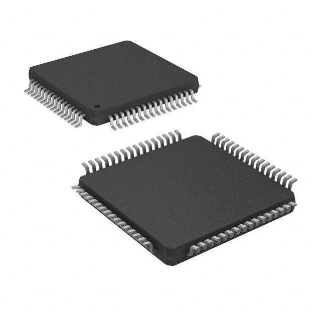
ORDERING INFORMATION (1)
PRODUCT
PACKAGE-LEAD
PACKAGE
DESIGNATOR
VCA8617
TQFP-64
PAG
(1)
SPECIFIED
TEMPERATURE
RANGE
PACKAGE
MARKING
−40°C to +85°C
VCA8617PAG
ORDERING
NUMBER
TRANSPORT
MEDIA, QUANTITY
VCA8617PAGT
Tape and Reel, 250
VCA8617PAGR
Tape and Reel, 1500
For the most current package and ordering information, see the Package Option Addendum at the end of this document, or see the TI
web site at www.ti.com.
ABSOLUTE MAXIMUM RATINGS (1)
Over operating free-air temperature range unless otherwise noted.
+AVDD
+3.6V
Analog Input
−0.3V to +AVDD + 0.3V
Logic Input
−0.3V to +AVDD + 0.3V
Case Temperature
+100°C
Junction Temperature
+150°C
Storage Temperature
+150°C
Thermal Resistance, Junction-to-Ambient (θ JA)
66.6°C/W
Thermal Resistance, Junction-to-Case (θ JC)
(1)
2
4.3°C/W
Stresses above these ratings may cause permanent damage. Exposure to absolute maximum conditions for extended periods may
degrade device reliability. These are stress ratings only, and functional operation of the device at these or any other conditions beyond
those specified is not implied.
Submit Documentation Feedback
Copyright © 2004–2009, Texas Instruments Incorporated
Product Folder Link(s): VCA8617
�VCA8617
www.ti.com
SBOS308F – AUGUST 2004 – REVISED NOVEMBER 2009
ELECTRICAL CHARACTERISTICS: AVDD = DVDD = 3V
At TA = +25°C, load resistance = 1kΩ on each output to ground, unless otherwise noted. The input to the preamp (LNA) is
single-ended; pre-amp gain is fixed at +20dB, fIN = 2MHz, PG = 01, ATN = 00, and the output from the VCA is differential,
unless otherwise noted.
VCA8617
PARAMETER
CONDITIONS
MIN
TYP
MAX
UNIT
Input Voltage Noise (TGC, Full Signal Chain)
fIN = 5MHz
1.05
nV/√Hz
Input Voltage Noise (CW)
fIN = 5MHz
1.15
nV/√Hz
Input Resistance
4.5
kΩ
Input Capacitance
52
pF
Input Bias Current
1
nA
200
mVPP
PREAMPLIFIER (LNA)
Maximum Input Voltage (1)
Output Swing (Differential)
2
VPP
100
MHz
Gain
20
dB
Input Common-Mode Voltage
1.4
V
Bandwidth
ACCURACY
Gain Slope
0.2V − 1.7V, VCNTRL
Gain Error
0.2V − 1.7V, VCNTRL
Output Offset Voltage
18
dB/V
1.7
Differential
0.65
dB
mV
GAIN CONTROL INTERFACE
Input Voltage (VCACNTRL) Range
Input Resistance
Response Time
40dB Gain Change, PG = 11
0 to 2.0
V
1
MΩ
0.2
μs
POWER SUPPLY
Specified Operating Range
2.85
Power-Down Delay
3.15
μs
100
Operating All Channels
825
Power-Down
V
μs
5
Power-Up Delay
Power Dissipation (TGC Mode)
3.0
950
mW
9
mW
−3dB Cutoff (low-pass)
14.5
MHz
−3dB Cutoff (high-pass)
400
kHz
Slew Rate
300
V/µs
Output Impedance
10
Ω
Crosstalk
49
dB
Output Common-Mode Voltage
1.5
PROGRAMMABLE VGA AND LOW-PASS FILTER
Output Swing (Differential) (2)
V
2
VPP
3rd-Harmonic Distortion
–65
–50
dB
2nd-Harmonic Distortion
–60
–50
dB
Group Delay Variation
±3
ns
CONTINUOUS WAVE PROCESSOR
V/I Converter Transconductance
17
20
23
mA/V
Output Common-Mode Voltage
1.4
V
Maximum Output Swing
3.4
mAPP
(1)
(2)
Under conditions when input signal is within linear range of LNA.
Under conditions when signal is within linear range of output amplifier.
Submit Documentation Feedback
Copyright © 2004–2009, Texas Instruments Incorporated
Product Folder Link(s): VCA8617
3
�VCA8617
SBOS308F – AUGUST 2004 – REVISED NOVEMBER 2009
www.ti.com
ELECTRICAL CHARACTERISTICS: AVDD = DVDD = 3V (continued)
At TA = +25°C, load resistance = 1kΩ on each output to ground, unless otherwise noted. The input to the preamp (LNA) is
single-ended; pre-amp gain is fixed at +20dB, fIN = 2MHz, PG = 01, ATN = 00, and the output from the VCA is differential,
unless otherwise noted.
VCA8617
PARAMETER
CONDITIONS
MIN
TYP
MAX
UNIT
0
0.6
V
2.1
DVDD
V
±1
µA
25M
Hz
LOGIC INPUTS
VIN LOW (input low voltage)
VIN HIGH (input high voltage)
Input Current
Input Pin Capacitance
Clock Input Frequency
4
5
10k
Submit Documentation Feedback
pF
Copyright © 2004–2009, Texas Instruments Incorporated
Product Folder Link(s): VCA8617
�VCA8617
SBOS308F – AUGUST 2004 – REVISED NOVEMBER 2009
AGND
IN8
AVDD
CW0
CW2
CW4
CW6
CW8
AGND
AVDD
VCNTRL
VLNA
AGND
VREF
TQFP
IN7
Top View
AGND
www.ti.com
64
63
62
61
60
59
58
57
56
55
54
53
52
51
50
49
IN6
1
48 OUT8
AGND
2
47 OUT8
IN5
3
46 OUT7
AGND
4
45 OUT7
DVDD
5
44 OUT6
DGND
6
43 OUT6
DOUT
7
42 OUT5
CLK
8
DIN
9
40 OUT4
CS 10
39 OUT4
DGND 11
38 OUT3
DVDD 12
37 OUT3
AGND 13
36 OUT2
IN4 14
35 OUT2
AGND 15
34 OUT1
IN3 16
33 OUT1
41 OUT5
26
27
28
29
30
31
32
VCM
GNDR
VDDR
AVDD
25
VFIL
IN1
24
AVDD
AGND
23
AGND
IN2
22
CW9
21
CW7
20
CW5
19
CW3
18
CW1
17
AGND
VCA8617
PIN DESCRIPTIONS
PIN
DESIGNATOR
DESCRIPTION
5, 12
DVDD
Digital Supplies
2, 4, 13, 15, 17, 19, 27, 50, 54, 62, 64
AGND
Analog Ground
1, 3, 14, 16, 18, 20, 61, 63
IN(1−8)
Single-Ended LNA Inputs
22−26, 55−59
CW(0−9)
Continuous Wave Outputs
51
VLNA
Reference Voltage for LNA−internally generated; requires external bypass cap.
29
VFIL
Reference Voltage for Output Filter−internally generated; requires external bypass cap.
30
VCM
Common-Mode Voltage−internally generated; requires external bypass cap.
34, 36, 38, 40, 42, 44, 46, 48
OUT(1−8)
Positive Polarity PGA Outputs
33, 35, 37, 39, 41, 43, 45, 47
OUT(1−8)
Negative Polarity PGA Outputs
52
VCNTRL
9
DIN
Serial Data Input Pin
10
CS
Serial Data Chip Select
8
CLK
Serial Data Input Clock
7
DOUT
Serial Data Output Pin
21, 28, 53, 60
AVDD
Analog Supplies
6, 11
DGND
Digital Ground
49
VREF
Reference Voltage for Attenuator−internally generated; requires external bypass cap.
32
VDDR
Reference Power Supply
31
GNDR
Attenuator Control Input
Reference Ground
Submit Documentation Feedback
Copyright © 2004–2009, Texas Instruments Incorporated
Product Folder Link(s): VCA8617
5
�VCA8617
SBOS308F – AUGUST 2004 – REVISED NOVEMBER 2009
www.ti.com
INPUT REGISTER BIT MAPS
Table 1. Byte 1—Control Byte Register Map
BIT #
NAME
LSB
1
DESCRIPTION
1
W/R
1 = Write, 0 = Read—Read prevents latching of DATA only—Control register remains
latched with existing data.
2
PWR
Power-Down control bit (all channels); 1 = Power-Down Mode Enabled (default),
0 = Normal Operation.
3
A0
Attenuator control bit (ATN).
4
A1
Attenuator control bit (ATN).
5
Mode
1 = TGC Control mode (CW powered down), 0 = Doppler mode (TGC powered down)
6
PG0
LSB of PGA Gain Control
MSB
PG1
MSB of PGA Gain Control
Start bit; always a ‘1’—40-bit countdown starts upon first ‘1’ after chip select.
Table 2. Byte 2—First Data Byte
BIT #
NAME
LSB
Data 1:0
DESCRIPTION
Channel 1, LSB of Matrix Control
1
Data 1:1
Channel 1, Matrix Control
2
Data 1:2
Channel 1, Matrix Control
3
Data 1:3
Channel 1, MSB of Matrix Control
4
Data 2:0
Channel 2, LSB of Matrix Control
5
Data 2:1
Channel 2, Matrix Control
6
Data 2:2
Channel 2, Matrix Control
MSB
Data 2:3
Channel 2, MSB of Matrix Control
BIT #
NAME
LSB
Data 3:0
Channel 3, LSB of Matrix Control
1
Data 3:1
Channel 3, Matrix Control
2
Data 3:2
Channel 3, Matrix Control
3
Data 3:3
Channel 3, MSB of Matrix Control
4
Data 4:0
Channel 4, LSB of Matrix Control
5
Data 4:1
Channel 4, Matrix Control
6
Data 4:2
Channel 4, Matrix Control
MSB
Data 4:3
Channel 4, MSB of Matrix Control
Table 3. Byte 3—Second Data Byte
6
DESCRIPTION
Submit Documentation Feedback
Copyright © 2004–2009, Texas Instruments Incorporated
Product Folder Link(s): VCA8617
�VCA8617
www.ti.com
SBOS308F – AUGUST 2004 – REVISED NOVEMBER 2009
Table 4. Byte 4—Third Data Byte
BIT #
NAME
LSB
Data 5:0
DESCRIPTION
Channel 5, LSB of Matrix Control
1
Data 5:1
Channel 5, Matrix Control
2
Data 5:2
Channel 5, Matrix Control
3
Data 5:3
Channel 5, MSB of Matrix Control
4
Data 6:0
Channel 6, LSB of Matrix Control
5
Data 6:1
Channel 6, Matrix Control
6
Data 6:2
Channel 6, Matrix Control
MSB
Data 6:3
Channel 6, MSB of Matrix Control
Table 5. Byte 5—Fourth Data Byte
BIT #
NAME
LSB
Data 7:0
DESCRIPTION
Channel 7, LSB of Matrix Control
1
Data 7:1
Channel 7, Matrix Control
2
Data 7:2
Channel 7, Matrix Control
3
Data 7:3
Channel 7, MSB of Matrix Control
4
Data 8:0
Channel 8, LSB of Matrix Control
5
Data 8:1
Channel 8, Matrix Control
6
Data 8:2
Channel 8, Matrix Control
MSB
Data 8:3
Channel 8, MSB of Matrix Control
Submit Documentation Feedback
Copyright © 2004–2009, Texas Instruments Incorporated
Product Folder Link(s): VCA8617
7
�VCA8617
SBOS308F – AUGUST 2004 – REVISED NOVEMBER 2009
www.ti.com
WRITE/READ TIMING
Generally follows SPI Timing Specification:
• All writes and reads are 40 bits at a time. Each byte consists of 8 bits;
• Separate write and read data lines;
• Reads will follow the same bit stream pattern seen in the write cycle;
• Reads will extract data from the FIFO, not the latched register;
• DOUT data is continuously available and need not be enabled with a read cycle. Selecting a read cycle in the
control register only prevents latching of data. The control register remains latched.
WRITE CYCLE TIMING
t4
CS
t7
t2
t3
CLK
t5
DIN
LSB
1
t6
t1
2
3
4
5
6
MSB
NOTE: It is highly recommended that the clock be turned off after the required data has been programmed into the VCA8617.
SERIAL PORT TIMING TABLE
Chip Select (CS) must be held low (active LOW) during transfer. CS can be held permanently low.
PARAMETER
8
DESCRIPTION
MIN
t1
Serial CLK Period
40
ns
t2
Serial CLK HIGH Time
20
ns
t3
Serial CLK LOW Time
20
ns
t4
CS Falling Edge to Serial CLK Falling Edge
10
ns
t5
Data Setup Time
5
ns
t6
Data Hold Time
5
ns
t7
Serial CLK Falling Edge to CS Rising Edge
10
ns
Submit Documentation Feedback
TYP
MAX
UNITS
Copyright © 2004–2009, Texas Instruments Incorporated
Product Folder Link(s): VCA8617
�VCA8617
www.ti.com
SBOS308F – AUGUST 2004 – REVISED NOVEMBER 2009
DATA SHIFT SEQUENCE
Shift Direction
DIN
MSB
6
5
4
3
2
1
LSB
MSB
6
5
4
3
2
1
LSB
MSB
6
5
4
3
2
1
LSB
MSB
6
5
4
3
2
1
LSB
MSB
6
5
4
3
2
1
LSB
Table 6. Maximum Attenuation
DOUT
Table 7. PGA Gain Settings
A1, A0
MAXIMUM ATTENUATION
PG1, PG0
PGA GAIN
0, 0
29dB
0, 0
25dB
0, 1
33dB
0, 1
30dB
1, 0
36.5dB
1, 0
35dB
1, 1
40dB
1, 1
40dB
Table 8. CW Coding for Each Channel
CHANNEL
CW CODING
(MSB, LSB)
0
0000
Output 0
1
0001
Output 1
2
0010
Output 2
3
0011
Output 3
4
0100
Output 4
5
0101
Output 5
6
0110
Output 6
7
0111
Output 7
8
1000
Output 8
9
1001
Output 9
10
1010
Channel tied to +V (internal)
11
1011
Channel tied to +V (internal)
12
1100
Channel tied to +V (internal)
13
1101
Channel tied to +V (internal)
14
1110
Channel tied to +V (internal)
15
1111
CHANNEL DIRECTED TO:
Channel tied to +V (internal)
Applies to bytes 2 through 5.
Submit Documentation Feedback
Copyright © 2004–2009, Texas Instruments Incorporated
Product Folder Link(s): VCA8617
9
�VCA8617
SBOS308F – AUGUST 2004 – REVISED NOVEMBER 2009
www.ti.com
TYPICAL CHARACTERISTICS: AVDD = DVDD = 3V
At TA = +25°C, load resistance = 1kΩ on each output to ground; the input to the preamp (LNA) is single-ended; pre-amp gain
is fixed at +20dB, fIN = 2MHz, PG = 01, ATN = 00, and the output from the VCA is differential, unless otherwise noted.
GAIN vs VCNTRL
(PG = 00, 25dB)
60
55
55
50
50
45
45
40
40
ATN = 00
35
30
25
Gain (dB)
Gain (dB)
GAIN vs VCNTRL
(PG = 01, 30dB)
ATN = 01
ATN = 11
0
0.2 0.3 0.4 0.5 0.6 0.7 0.8 0.9 1.0 1.1 1.2 1.3 1.4 1.5 1.6 1.7
VCNTRL (V)
VCNTRL (V)
Figure 1.
Figure 2.
GAIN vs VCNTRL
(PG = 10, 35dB)
GAIN vs VCNTRL
(PG = 11, 40dB)
ATN = 00
50
45
Gain (dB)
Gain (dB)
ATN = 01
30
ATN = 11
25
20
10
ATN = 10
0.2 0.3 0.4 0.5 0.6 0.7 0.8 0.9 1.0 1.1 1.2 1.3 1.4 1.5 1.6 1.7
55
15
ATN = 11
5
ATN = 10
60
35
25
10
10
40
ATN = 01
30
15
15
0
35
20
20
5
ATN = 00
ATN = 10
5
0
0.2 0.3 0.4 0.5 0.6 0.7 0.8 0.9 1.0 1.1 1.2 1.3 1.4 1.5 1.6 1.7
65
60
55
50
45
40
35
30
25
20
15
10
5
0
ATN = 00
ATN = 01
ATN = 11
ATN = 10
0.2 0.3 0.4 0.5 0.6 0.7 0.8 0.9 1.0 1.1 1.2 1.3 1.4 1.5 1.6 1.7
VCNTRL (V)
VCNTRL (V)
Figure 3.
10
Figure 4.
Submit Documentation Feedback
Copyright © 2004–2009, Texas Instruments Incorporated
Product Folder Link(s): VCA8617
�VCA8617
www.ti.com
SBOS308F – AUGUST 2004 – REVISED NOVEMBER 2009
TYPICAL CHARACTERISTICS: AVDD = DVDD = 3V (continued)
At TA = +25°C, load resistance = 1kΩ on each output to ground; the input to the preamp (LNA) is single-ended; pre-amp gain
is fixed at +20dB, fIN = 2MHz, PG = 01, ATN = 00, and the output from the VCA is differential, unless otherwise noted.
GAIN ERROR vs VCNTRL
(PG = 01)
2.0
2.0
1.5
1.5
1.0
1.0
0.5
ATN = 01
Gain Error (dB)
Gain Error (dB)
GAIN ERROR vs VCNTRL
(PG = 00)
ATN = 00
0
ATN = 10
− 0.5
− 1.0
ATN = 01
ATN = 00
0.5
0
ATN = 11
− 0.5
ATN = 10
− 1.0
− 1.5
− 1.5
ATN = 11
− 2.0
0.2 0.3 0.4 0.5 0.6 0.7 0.8 0.9 1.0 1.1 1.2 1.3 1.4 1.5 1.6 1.7
VCNTRL (V)
VCNTRL (V)
Figure 5.
Figure 6.
GAIN ERROR vs VCNTRL
(PG = 10)
GAIN ERROR vs VCNTRL
(PG = 11)
2.0
2.0
1.5
1.5
0.5
ATN = 00
0
− 0.5
ATN = 11
ATN = 00
0.5
0
− 0.5
ATN = 10
− 1.0
− 1.0
− 1.5
ATN = 01
1.0
ATN = 01
Gain Error (dB)
1.0
Gain Error (dB)
− 2.0
0.2 0.3 0.4 0.5 0.6 0.7 0.8 0.9 1.0 1.1 1.2 1.3 1.4 1.5 1.6 1.7
− 1.5
ATN = 10
− 2.0
ATN = 11
− 2.0
0.2 0.3 0.4 0.5 0.6 0.7 0.8 0.9 1.0 1.1 1.2 1.3 1.4 1.5 1.6 1.7
0.2 0.3 0.4 0.5 0.6 0.7 0.8 0.9 1.0 1.1 1.2 1.3 1.4 1.5 1.6 1.7
VCNTRL (V)
VCNTRL (V)
Figure 7.
Figure 8.
GAIN ERROR vs VCNTRL vs FREQUENCY
GAIN ERROR vs VCNTRLvs TEMPERATURE
2.0
10MHz
1.5
5MHz
0.5
2MHz
0
− 0.5
− 1.0
− 1.5
− 2.0
Gain (dB)
Gain Error (dB)
1.0
2.0
1.8
1.6
1.4
1.2
1.0
0.8
0.6
0.4
0.2
0
-0.2
-0.4
-0.6
-0.8
-1.0
+85°C
+25°C
-40°C
0.2 0.3 0.4 0.5 0.6 0.7 0.8 0.9 1.0 1.1 1.2 1.3 1.4 1.5 1.6 1.7
0.2 0.3 0.4 0.5 0.6 0.7 0.8 0.9 1.0 1.1 1.2 1.3 1.4 1.5 1.6 1.7
VCNTRL (V)
VCNTRL (V)
Figure 9.
Figure 10.
Submit Documentation Feedback
Copyright © 2004–2009, Texas Instruments Incorporated
Product Folder Link(s): VCA8617
11
�VCA8617
SBOS308F – AUGUST 2004 – REVISED NOVEMBER 2009
www.ti.com
TYPICAL CHARACTERISTICS: AVDD = DVDD = 3V (continued)
At TA = +25°C, load resistance = 1kΩ on each output to ground; the input to the preamp (LNA) is single-ended; pre-amp gain
is fixed at +20dB, fIN = 2MHz, PG = 01, ATN = 00, and the output from the VCA is differential, unless otherwise noted.
CONTINUOUS WAVE (CW) CURRENT
vs TEMPERATURE
220
285
284
283
282
281
280
279
278
277
276
275
274
273
272
271
270
269
268
218
216
214
CW Current (mA)
TGC Current (mA)
TIME GAIN CONTROL (TGC) CURRENT
vs TEMPERATURE
212
210
208
206
204
202
200
198
196
− 40
− 20
0
20
40
60
− 40
80
0
20
40
60
80
Temperature (°C)
GAIN MATCH
(VCNTRL = 0.2V)
GAIN MATCH
(VCNTRL = 1.7V)
140
120
120
100
100
80
80
Units
140
60
40
40
20
20
0
0
0.02
0.11
0.21
0.30
0.39
0.49
0.58
0.67
0.77
0.86
0.95
1.05
1.14
1.23
60
− 0.81
−0.75
−0.68
−0.62
−0.55
− 0.48
−0.42
−0.35
−0.28
−0.22
− 0.15
−0.08
0.05
0.12
0.18
0.25
0.32
0.38
0.45
0.52
0.58
0.65
0.71
0.78
0.85
0.91
0.98
Figure 12.
Delta Gain (dB)
Delta Gain (dB)
Figure 13.
12
− 20
Figure 11.
− 1.28
− 1.19
− 1.10
− 1.00
− 0.91
− 0.82
− 0.72
− 0.63
− 0.54
− 0.44
− 0.35
− 0.26
− 0.16
− 0.07
Units
Temperature (°C)
Figure 14.
Submit Documentation Feedback
Copyright © 2004–2009, Texas Instruments Incorporated
Product Folder Link(s): VCA8617
�VCA8617
www.ti.com
SBOS308F – AUGUST 2004 – REVISED NOVEMBER 2009
TYPICAL CHARACTERISTICS: AVDD = DVDD = 3V (continued)
At TA = +25°C, load resistance = 1kΩ on each output to ground; the input to the preamp (LNA) is single-ended; pre-amp gain
is fixed at +20dB, fIN = 2MHz, PG = 01, ATN = 00, and the output from the VCA is differential, unless otherwise noted.
GAIN vs FREQUENCY
(ATN = 00, VCNTRL = 0.2V)
CW ACCURACY
900
800
700
Gain (dB)
Units
600
500
400
300
200
100
0
50
45
40
35
30
25
20
15
10
5
0
−5
− 10
− 15
PG = 11
PG = 10
PG = 00
PG = 01
18.1
18.2
18.3
18.4
18.5
18.7
18.8
18.9
19.0
19.1
19.3
19.4
19.5
19.6
19.7
19.9
20.0
20.1
20.2
20.3
20.5
20.6
20.7
20.8
20.9
21.1
21.2
21.3
0.1
1
Transconductance (mA/V)
Figure 16.
GAIN vs FREQUENCY
(ATN = 00, VCNTRL = 1.7V)
OUTPUT-REFERRED NOISE vs VCNTRL
(ATN = 00, fIN = 2MHz)
PG = 11
PG = 10
Noise (nV/ÖHz)
55
Gain (dB)
50
45
40
35
PG = 01
PG = 00
30
25
20
0.1
100
Figure 15.
65
60
10
Frequency (MHz)
1
10
100
1300
1200
1100
1000
900
800
700
600
500
400
300
200
100
0
PG = 11
PG = 10
PG = 01
PG = 00
0.2
0.4
0.6
0.8
1.0
1.2
1.4
1.6
1.8
2.0
VCNTRL (V)
Frequency (MHz)
Figure 17.
Figure 18.
Submit Documentation Feedback
Copyright © 2004–2009, Texas Instruments Incorporated
Product Folder Link(s): VCA8617
13
�VCA8617
SBOS308F – AUGUST 2004 – REVISED NOVEMBER 2009
www.ti.com
TYPICAL CHARACTERISTICS: AVDD = DVDD = 3V (continued)
At TA = +25°C, load resistance = 1kΩ on each output to ground; the input to the preamp (LNA) is single-ended; pre-amp gain
is fixed at +20dB, fIN = 2MHz, PG = 01, ATN = 00, and the output from the VCA is differential, unless otherwise noted.
OUTPUT-REFERRED NOISE vs VCNTRL
(ATN = 00, fIN = 5MHz)
INPUT-REFERRED NOISE vs VCNTRL
(ATN = 00, fIN = 2MHz)
20
1200
1100
1000
PG = 11
16
800
Noise (nV/ÖHz)
900
Noise (nV/ÖHz)
PG = 00
18
PG = 11
PG = 10
700
600
500
PG = 01
400
300
14
12
10
PG = 01
8
6
PG = 10
4
200
2
100
PG = 00
0
0.2
0.4
0.6
0.8
1.0
1.2
1.4
1.6
1.8
0
0.2
2.0
0.4
0.6
0.8
1.4
1.6
1.8
2.0
Figure 20.
INPUT-REFERRED NOISE vs VCNTRL
(ATN = 00, fIN = 5MHz)
NOISE FIGURE vs VCNTRL
(ATN = 00, fIN = 2MHz)
1.6
1.8
2.0
30
PG = 00
25
PG = 00
PG = 11
PG = 01
PG = 01
20
PG = 11
PG = 10
15
10
5
PG = 10
0
0.2
0.4
0.6
0.8
1.0
1.2
1.4
1.6
1.8
2.0
0.2
0.4
0.6
0.8
1.0
1.2
1.4
VCNTRL (V)
VCNTRL (V)
Figure 21.
14
1.2
Figure 19.
Noise Figure (dB)
Noise (nV/ÖHz)
18
17
16
15
14
13
12
11
10
9
8
7
6
5
4
3
2
1
0
1.0
VCNTRL (V)
VCNTRL (V)
Figure 22.
Submit Documentation Feedback
Copyright © 2004–2009, Texas Instruments Incorporated
Product Folder Link(s): VCA8617
�VCA8617
www.ti.com
SBOS308F – AUGUST 2004 – REVISED NOVEMBER 2009
TYPICAL CHARACTERISTICS: AVDD = DVDD = 3V (continued)
At TA = +25°C, load resistance = 1kΩ on each output to ground; the input to the preamp (LNA) is single-ended; pre-amp gain
is fixed at +20dB, fIN = 2MHz, PG = 01, ATN = 00, and the output from the VCA is differential, unless otherwise noted.
NOISE FIGURE vs VCNTRL
(ATN = 00, fIN = 5MHz)
OUTPUT-REFERRED NOISE vs VCNTRL
(ATN = 11, fIN = 2MHz)
1200
30
1100
PG = 00
1000
25
20
900
Noise (nV/ÖHz)
Noise Figure (dB)
PG = 11
PG = 01
15
PG = 10
10
800
700
PG = 11
600
500
PG = 10
400
300
PG = 01
200
5
100
PG = 00
0
0
0.2
0.4
0.6
0.8
1.0
1.2
1.4
1.6
1.8
2.0
0.2
0.4
0.6
0.8
VCNTRL (V)
1.2
1.4
1.6
Figure 23.
Figure 24.
OUTPUT-REFERRED NOISE vs VCNTRL
(ATN = 11, fIN = 5MHz)
INPUT-REFERRED NOISE vs VCNTRL
(ATN = 11, fIN = 2MHz)
1100
1.8
2.0
80
PG = 00
1000
70
900
PG = 01
60
700
PG = 11
600
500
400
PG = 01
PG = 10
300
Noise (nV/ÖHz)
800
Noise (nV/ÖHz)
1.0
VCNTRL (V)
50
40
30
PG = 11
20
200
PG = 10
10
100
PG = 00
0
0.2
0.4
0.6
0.8
1.0
1.2
1.4
1.6
1.8
2.0
0
0.2
0.4
0.6
0.8
1.0
1.2
1.4
1.6
1.8
2.0
VCNTRL (V)
VCNTRL (V)
Figure 25.
Figure 26.
Submit Documentation Feedback
Copyright © 2004–2009, Texas Instruments Incorporated
Product Folder Link(s): VCA8617
15
�VCA8617
SBOS308F – AUGUST 2004 – REVISED NOVEMBER 2009
www.ti.com
TYPICAL CHARACTERISTICS: AVDD = DVDD = 3V (continued)
At TA = +25°C, load resistance = 1kΩ on each output to ground; the input to the preamp (LNA) is single-ended; pre-amp gain
is fixed at +20dB, fIN = 2MHz, PG = 01, ATN = 00, and the output from the VCA is differential, unless otherwise noted.
INPUT-REFERRED NOISE vs VCNTRL
(ATN = 11, fIN = 5MHz)
NOISE FIGURE vs VCNTRL
(ATN = 11, fIN = 2MHz)
70
40
PG = 00
Noise Figure (dB)
Noise (nV/ÖHz)
PG = 01
50
PG = 10
40
30
20
PG = 00
35
60
PG = 11
30
PG = 01
25
20
PG = 11
15
10
10
PG = 10
5
0
0
0.2
0.4
0.6
0.8
1.0
1.2
1.4
1.6
1.8
0.2
2.0
0.4
0.6
1.0
1.2
1.4
Figure 27.
Figure 28.
NOISE FIGURE vs VCNTRL
(ATN = 11, fIN = 5MHz)
INPUT-REFERRED NOISE
(2MHz, 2V VCNTRL)
40
1.6
1.8
2.0
1.25
AT00
PG = 00
35
AT11
1.20
30
PG = 01
Noise (nV/√Hz)
Noise Figure (dB)
0.8
VCNTRL (V)
VCNTRL (V)
25
20
PG = 11
15
PG = 10
1.15
1.10
10
1.05
5
0
1.00
0.2
0.4
0.6
0.8
1.0
1.2
1.4
1.6
1.8
2.0
VCNTRL (V)
PG 01
PG 10
PG 11
Gain Setting
Figure 29.
16
PG 00
Figure 30.
Submit Documentation Feedback
Copyright © 2004–2009, Texas Instruments Incorporated
Product Folder Link(s): VCA8617
�VCA8617
www.ti.com
SBOS308F – AUGUST 2004 – REVISED NOVEMBER 2009
TYPICAL CHARACTERISTICS: AVDD = DVDD = 3V (continued)
At TA = +25°C, load resistance = 1kΩ on each output to ground; the input to the preamp (LNA) is single-ended; pre-amp gain
is fixed at +20dB, fIN = 2MHz, PG = 01, ATN = 00, and the output from the VCA is differential, unless otherwise noted.
INPUT-REFERRED NOISE
(5MHz, 2V VCNTRL)
INPUT-REFERRED NOISE
(CW Output)
2.00
1.10
AT00
AT11
1.90
Noise (nV/√Hz)
Noise (nV/√Hz)
1.80
1.05
1.70
1.60
1.50
1.40
1.30
1.20
1.10
1.00
1.00
PG 00
PG 01
PG 10
1
PG 11
4
Figure 32.
DISTORTION vs FREQUENCY
(ATN = 00, PG = 00, VCNTL = 2.0V)
DISTORTION vs FREQUENCY
(ATN = 00, PG = 01, VCNTL = 2.0V)
− 30
− 35
− 35
− 40
− 40
− 45
− 45
Distortion (dBc)
Distortion (dB)
3
Figure 31.
− 30
− 50
− 55
2
2nd−Harmonic
− 60
− 65
− 70
5
Frequency (MHz)
Gain Setting
− 50
2nd−Harmonic
− 55
− 60
− 65
− 70
3rd−Harmonic
− 75
3rd−Harmonic
− 75
− 80
− 80
1
10
1
Frequency (MHz)
10
Frequency (MHz)
Figure 33.
Figure 34.
Submit Documentation Feedback
Copyright © 2004–2009, Texas Instruments Incorporated
Product Folder Link(s): VCA8617
17
�VCA8617
SBOS308F – AUGUST 2004 – REVISED NOVEMBER 2009
www.ti.com
TYPICAL CHARACTERISTICS: AVDD = DVDD = 3V (continued)
At TA = +25°C, load resistance = 1kΩ on each output to ground; the input to the preamp (LNA) is single-ended; pre-amp gain
is fixed at +20dB, fIN = 2MHz, PG = 01, ATN = 00, and the output from the VCA is differential, unless otherwise noted.
DISTORTION vs FREQUENCY
(ATN = 00, PG = 11, VCNTL = 2.0V)
− 30
− 30
− 35
− 35
− 40
− 40
− 45
− 45
Distortion (dB)
Distortion (dB)
DISTORTION vs FREQUENCY
(ATN = 00, PG = 10, VCNTL = 2.0V)
− 50
− 55
− 60
2nd−Harmonic
− 65
− 50
2nd−Harmonic
− 55
− 60
− 65
3rd−Harmonic
− 70
− 70
− 75
− 75
− 80
3rd−Harmonic
− 80
1
10
1
10
Frequency (MHz)
Figure 35.
Figure 36.
DISTORTION vs VCNTRL
(ATN = 00, PG = 10, fIN = 2MHz, 750mVPP)
DISTORTION vs VCNTRL
(ATN = 01, PG = 10, fIN = 2MHz, 750mVPP)
-30
-30
-35
-35
-40
-40
-45
-45
Distortion (dB)
Distortion (dB)
Frequency (MHz)
-50
-55
-60
2nd-Harmonic
-65
-50
-55
-60
2nd-Harmonic
-65
-70
-70
3rd-Harmonic
-75
3rd-Harmonic
-75
-80
-80
0.2
0.5
0.8
1.1
1.4
1.7
2.0
0.2
VCNTRL (V)
0.8
1.1
1.4
1.7
2.0
VCNTRL (V)
Figure 37.
18
0.5
Figure 38.
Submit Documentation Feedback
Copyright © 2004–2009, Texas Instruments Incorporated
Product Folder Link(s): VCA8617
�VCA8617
www.ti.com
SBOS308F – AUGUST 2004 – REVISED NOVEMBER 2009
TYPICAL CHARACTERISTICS: AVDD = DVDD = 3V (continued)
At TA = +25°C, load resistance = 1kΩ on each output to ground; the input to the preamp (LNA) is single-ended; pre-amp gain
is fixed at +20dB, fIN = 2MHz, PG = 01, ATN = 00, and the output from the VCA is differential, unless otherwise noted.
DISTORTION vs VCNTRL
(ATN = 11, PG = 10, fIN = 2MHz, 750mVPP)
-30
-30
-35
-35
-40
-40
-45
-45
Distortion (dB)
-50
-55
-60
2nd-Harmonic
Under this test condition, at lower VCA
control voltage, the LNA is overloaded.
-50
-55
-60
2nd-Harmonic
-65
-65
-70
-70
3rd-Harmonic
3rd-Harmonic
-75
-75
-80
-80
0.2
0.5
0.8
1.1
1.4
1.7
2.0
0.2
0.3
0.4
0.5
0.6
0.7
0.8
0.9
1.0
1.1
1.2
1.3
1.4
1.5
1.6
1.7
1.8
1.9
2.0
Distortion (dB)
DISTORTION vs VCNTRL
(ATN = 10, PG = 10, fIN = 2MHz, 750mVPP)
VCNTRL (V)
Figure 39.
Figure 40.
DISTORTION vs VCNTRL
(ATN = 00, PG = 00, 500mVPP, 2nd-Harmonic)
DISTORTION vs VCNTRL
(ATN = 00, PG = 01, 500mVPP, 2nd-Harmonic)
-30
-30
-35
-35
-40
-40
-45
10MHz
-50
-55
-60
5MHz
-65
10MHz
-50
-55
5MHz
-60
2MHz
-70
2MHz
1MHz
-75
-80
1MHz
0.2
0.3
0.4
0.5
0.6
0.7
0.8
0.9
1.0
1.1
1.2
1.3
1.4
1.5
1.6
1.7
1.8
1.9
2.0
0.2
0.3
0.4
0.5
0.6
0.7
0.8
0.9
1.0
1.1
1.2
1.3
1.4
1.5
1.6
1.7
1.8
1.9
2.0
-80
-45
-65
-70
-75
Distortion (dB)
Distortion (dB)
VCNTRL (V)
VCNTRL (V)
VCNTRL (V)
Figure 41.
Figure 42.
Submit Documentation Feedback
Copyright © 2004–2009, Texas Instruments Incorporated
Product Folder Link(s): VCA8617
19
�VCA8617
SBOS308F – AUGUST 2004 – REVISED NOVEMBER 2009
www.ti.com
TYPICAL CHARACTERISTICS: AVDD = DVDD = 3V (continued)
At TA = +25°C, load resistance = 1kΩ on each output to ground; the input to the preamp (LNA) is single-ended; pre-amp gain
is fixed at +20dB, fIN = 2MHz, PG = 01, ATN = 00, and the output from the VCA is differential, unless otherwise noted.
DISTORTION vs VCNTRL
(ATN = 00, PG = 10, 500mVPP, 2nd-Harmonic)
DISTORTION vs VCNTRL
(ATN = 00, PG = 10, 500mVPP, 2nd-Harmonic)
30
30
35
35
40
10MHz
45
50
55
60
5MHz
2MHz
65
Distortion (dB)
10MHz
45
50
55
60
70
70
75
75
1MHz
1MHz
1.7
1.8
1.9
2.0
0.2
0.3
0.4
0.5
0.6
0.7
0.2
0.3
0.4
0.5
0.6
0.7
0.8
0.9
1.0
1.1
1.2
1.3
1.4
1.5
1.6
1.7
1.8
1.9
2.0
VCNTRL (V)
VCNTRL (V)
Figure 43.
Figure 44.
DISTORTION vs VCNTRL
(ATN = 00, PG = 00, 500mVPP, 3rd-Harmonic)
DISTORTION vs VCNTRL
(ATN = 00, PG = 01, 500mVPP, 3rd-Harmonic)
− 30
− 30
− 35
− 35
− 40
− 40
2MHz
− 50
10MHz
− 55
− 60
5MHz
− 50
10MHz
− 55
− 60
5MHz
− 65
1MHz
− 70
− 80
1.7
1.8
1.9
2.0
− 80
0.8
0.9
1.0
1.1
1.2
1.3
1.4
1.5
1.6
− 75
0.2
0.3
0.4
0.5
0.6
0.7
− 75
2MHz
1MHz
1.7
1.8
1.9
2.0
− 65
− 70
− 45
0.2
0.3
0.4
0.5
0.6
0.7
− 45
Distortion (dB)
Distortion (dB)
0.8
0.9
1.0
1.1
1.2
1.3
1.4
1.5
1.6
80
80
VCNTRL (V)
VCNTRL (V)
Figure 45.
20
5MHz
2MHz
65
0.8
0.9
1.0
1.1
1.2
1.3
1.4
1.5
1.6
Distortion (dB)
40
Figure 46.
Submit Documentation Feedback
Copyright © 2004–2009, Texas Instruments Incorporated
Product Folder Link(s): VCA8617
�VCA8617
www.ti.com
SBOS308F – AUGUST 2004 – REVISED NOVEMBER 2009
TYPICAL CHARACTERISTICS: AVDD = DVDD = 3V (continued)
At TA = +25°C, load resistance = 1kΩ on each output to ground; the input to the preamp (LNA) is single-ended; pre-amp gain
is fixed at +20dB, fIN = 2MHz, PG = 01, ATN = 00, and the output from the VCA is differential, unless otherwise noted.
DISTORTION vs VCNTRL
(ATN = 00, PG = 11, 500mVPP, 3rd-Harmonic)
30
30
35
35
40
40
45
45
60
5MHz
65
50
10MHz
55
60
5MHz
65
70
70
2MHz
75
1MHz
1MHz
80
0.2
0.3
0.4
0.5
0.6
0.7
1.2
1.3
1.4
1.5
1.6
1.7
1.8
1.9
2.0
0.8
0.9
1.0
1.1
VCNTRL (V) )
Figure 47.
Figure 48.
CROSSTALK vs VCNTRL
(ATN = 00, fIN = 2MHz, CH4 to CH5)
CROSSTALK vs VCNTRL
(ATN = 00, fIN = 5MHz, CH4 to CH5)
− 30
− 35
− 35
− 40
− 40
PG10
− 50
− 55
− 60
PG = 01
PG = 00
− 45
− 50
PG = 00
− 60
− 65
− 65
− 70
− 70
0.2
PG = 01
− 55
0.3
0.4
0.5
0.6
0.7
0.8
0.9
1.0
1.1
PG11
PG10
PG11
0.2
− 45
Crosstalk (dB)
− 30
0.3
0.4
0.5
0.6
0.7
0.8
0.9
1.0
1.1
1.2
1.3
1.4
1.5
1.6
1.7
1.8
1.9
2.0
Crosstalk (dB)
VCNTRL (V)
VCNTRL (V)
1.2
1.3
1.4
1.5
1.6
1.7
1.8
1.9
2.0
0.2
0.3
0.4
0.5
0.6
0.7
80
2MHz
75
1.7
1.8
1.9
2.0
10MHz
55
0.8
0.9
1.0
1.1
1.2
1.3
1.4
1.5
1.6
50
Distortion (dB)
Distortion (dB)
DISTORTION vs VCNTRL
(ATN = 00, PG = 10, 500mVPP, 3rd-Harmonic)
VCNTRL (V)
Figure 49.
Figure 50.
Submit Documentation Feedback
Copyright © 2004–2009, Texas Instruments Incorporated
Product Folder Link(s): VCA8617
21
�VCA8617
SBOS308F – AUGUST 2004 – REVISED NOVEMBER 2009
www.ti.com
TYPICAL CHARACTERISTICS: AVDD = DVDD = 3V (continued)
At TA = +25°C, load resistance = 1kΩ on each output to ground; the input to the preamp (LNA) is single-ended; pre-amp gain
is fixed at +20dB, fIN = 2MHz, PG = 01, ATN = 00, and the output from the VCA is differential, unless otherwise noted.
CROSSTALK vs VCNTRL
(ATN = 00, fIN = 10MHz, CH4 to CH5)
CROSSTALK to VCNTRL
(ATN = 11, PG = 11, CH4 to CH5)
− 30
− 30
− 35
Crosstalk (dB)
− 45
PG = 00
PG = 01
− 50
− 55
− 45
− 50
− 55
− 65
− 65
− 70
− 70
2MHz
0.2
0.3
0.4
0.5
0.6
0.7
1.2
1.3
1.4
1.5
1.6
1.7
1.8
1.9
2.0
− 60
0.8
0.9
1.0
1.1
− 60
0.3
0.4
0.5
0.6
0.7
10MHz
5MHz
− 40
0.2
Crosstalk (dB)
− 40
VCNTRL (V)
1.7
1.8
1.9
2.0
PG10
PG11
0.8
0.9
1.0
1.1
1.2
1.3
1.4
1.5
1.6
− 35
VCNTRL (V)
Figure 51.
Figure 52.
CROSSTALK to VCNTRL; CH1 vs CHn
(at 5MHz, AT = 00, PG = 00)
CROSSTALK to VCNTRL; CH1 vs CHn
(at 5MHz, AT = 11, PG = 00)
30
30
35
35
40
40
1-2
Crosstalk (dB)
Crosstalk (dB)
1-3
1-2
1-3 1-4
45
50
1-5
1-6
1-4
45
50
1-5 1-6
1-7
1-8
55
1-8
60
60
0
0.2
0.4
0.6
0.8
1.0
1.2
1.4
1.6
1.8
2.0
0
VCNTRL (V)
0.2
0.4
0.6
0.8
1.0
1.2
1.4
1.6
1.8
2.0
VCNTRL (V)
Figure 53.
22
1-7
55
Figure 54.
Submit Documentation Feedback
Copyright © 2004–2009, Texas Instruments Incorporated
Product Folder Link(s): VCA8617
�VCA8617
www.ti.com
SBOS308F – AUGUST 2004 – REVISED NOVEMBER 2009
TYPICAL CHARACTERISTICS: AVDD = DVDD = 3V (continued)
At TA = +25°C, load resistance = 1kΩ on each output to ground; the input to the preamp (LNA) is single-ended; pre-amp gain
is fixed at +20dB, fIN = 2MHz, PG = 01, ATN = 00, and the output from the VCA is differential, unless otherwise noted.
CROSSTALK to VCNTRL; CH1 vs CHn
(at 5MHz, AT = 11, PG = 11)
30
30
35
35
1-2
40
Crosstalk (dB)
Crosstalk (dB)
CROSSTALK to VCNTRL; CH1 vs CHn
(at 5MHz, AT = 00, PG = 11)
1-2
1-3
1-4
45
50
1-5
1-6
55
1-7 1-8
1-3
40
1-4
45
50
1-5
1-6
1-7
55
1-8
60
60
0
0.2
0.4
0.6
0.8
1.0
1.2
1.4
1.6
1.8
0
2.0
0.2
0.4
0.6
0.8
VCNTRL (V)
Figure 55.
1.2
1.4
1.6
1.8
2.0
Figure 56.
INPUT IMPEDANCE
INPUT IMPEDANCE
5000
0
4500
−10
4000
−20
3500
−30
Phase (_)
Magnitude (W)
1.0
VCNTRL (V)
3000
2500
2000
−40
−50
−60
1500
1000
−70
500
−80
−90
0
0.1
1
10
100
0.1
1
Frequency (MHz)
10
100
Frequency (MHz)
Figure 57.
Figure 58.
OVERLOAD RECOVERY vs TIME
(ATN = 00, PG = 00, VCNTRL = 1V)
OVERLOAD RECOVERY vs TIME
(ATN = 00, PG = 01, VCNTRL = 2V)
Output
(2V/div)
Output
(2V/div)
The signal is greater than 2VPP input, so the LNA is
severely overloaded. Overload recovery time is 528ns.
Input
(1V/div)
The signal is greater than 40mVPP input, so the LNA is in the linear region
and the output amplifier is overloaded. Overload recovery time is 400ns.
Input
(20mV/div)
Time (400ns/div)
Time (400ns/div)
Figure 59.
Figure 60.
Submit Documentation Feedback
Copyright © 2004–2009, Texas Instruments Incorporated
Product Folder Link(s): VCA8617
23
�VCA8617
SBOS308F – AUGUST 2004 – REVISED NOVEMBER 2009
www.ti.com
APPLICATION INFORMATION
NOTE: For current users of the VCA8613 who are
switching to the VCA8617, pin 32 of the VCA8617 is
a VDD reference pin and requires a minimum 0.1μF
bypass capacitor to ground.
INPUT CIRCUIT
to a little over 2VPP differential swing. This implies a
maximum input voltage swing of approximately
200mVPP to be operating in the linear range at 5MHz.
Larger input signals can be accepted by the LNA, but
distortion performance will degrade with larger input
signals.
The input of the VCA8617 integrates several
commonly-used elements. Before reaching the input
of the LNA, the receive signal should be coupled with
a capacitor of at least 10nF (preferably more). When
this ac-coupling element is inserted, the LNA input
bias point is held to a common-mode value of 1.4V
by an integrated 4.5kΩ resistor. This common-mode
value changes with temperature and may also vary
from chip to chip, but for each chip, it will be held
constant. Two back-to-back clipping diodes are in
parallel with this resistor. These diodes prevent
excessive input voltages from passing through to the
LNA input, preventing deep saturation effects in the
LNA itself. These integrated diodes are designed to
handle a dc-current of up to about 10mA. If the
application requires improved overload protection,
external Schottky diodes, such as the BAS40 series
by Infineon, should be considered.
CW DOPPLER PROCESSOR
LOW-NOISE PRE-AMPLIFIER (LNA)
The CW output common-mode is 1.4V.
The VCA8617 integrates a low-noise pre-amplifier.
Because of the high level of integration in the system,
noise performance was traded for power
consumption, resulting in an extremely low-power
pre-amplifier, with 0.8nV/√Hz noise performance at
5MHz. The LNA is configured as a fixed-gain 20dB
amplifier. Of this total gain, 6dB results from the
single-ended to differential conversion accomplished
within the LNA itself. The output of the LNA is limited
The CW outputs are typically routed to a passive
delay line, allowing coherent summing of the signals.
After summing, IQ separation and down conversion to
baseband precedes a pair of high-resolution, low
sample rate ADCs.
The VCA8617 integrates many of the elements
necessary to allow for the implementation of a simple
CW Doppler processing circuit. One circuit that was
integrated was a V/I converter following the LNA, as
shown in Figure 61. The V/I converter converts the
differential LNA voltage output to a current, which is
then passed through an 8x10 switch matrix (see
Figure 62). Within this switch matrix, any of the eight
LNA outputs can be connected to any of 10 CW
output
pins.
This
example
is
a
simple
current-summing circuit, such that each CW output
can represent the sum of any or all the channel
currents. The transconductance of the V/I converter is
approximately 20mA/V relative to the LNA input. For
proper operation of the CW Doppler Processor, it is
mandatory to have a bias voltage on the
output/outputs that are selected (see Figure 63).
VCM = 1.5V
Buffer
Cross-Point
Switch
LNA
20dB
Input 1
4.5kW
Buffer
VLNA
(+1.4V)
CW Output
Control
Logic
VCM = 1.5V
Figure 61. Basic CW Processing Block Diagram
24
Submit Documentation Feedback
Copyright © 2004–2009, Texas Instruments Incorporated
Product Folder Link(s): VCA8617
�VCA8617
www.ti.com
SBOS308F – AUGUST 2004 – REVISED NOVEMBER 2009
V/I
Converter
Channel 1
Input
CW0
CW1
SDI
CW2
CW3
Decode
Logic
CLK
CW4
CW5
CW6
SDO
CW7
CW8
CW9
+V
V/I
Converter
Channel 8
Input
SDI
Decode
Logic
SDO
Figure 62. Basic CW Cross-Point Switch Matrix for All Eight Channels
VCA8617
R
To CW Circuitry
CW Output
OPA
VBIAS = 1.2V to 1.6V
Figure 63. Operational Amplifier
Submit Documentation Feedback
Copyright © 2004–2009, Texas Instruments Incorporated
Product Folder Link(s): VCA8617
25
�VCA8617
SBOS308F – AUGUST 2004 – REVISED NOVEMBER 2009
www.ti.com
VOLTAGE-CONTROLLED ATTENUATOR
(VCA)—DETAIL
The VCA is designed to have a dB-linear attenuation
characteristic; that is, the gain loss in dB is constant
for each equal increment of the VCNTRL control
voltage. Figure 64 shows a block diagram of the
VCA. The attenuator is essentially a variable voltage
divider consisting of one series input resistor, RS, and
10 identical shunt FETs, placed in parallel and
controlled
by
sequentially-activated
clipping
amplifiers. Each clipping amplifier can be thought of
as a specialized voltage comparator with a soft
transfer characteristic and well-controlled output limit
voltages. The reference voltages V1 through V10 are
equally spaced over the 0V to 2.0V control voltage
range. As the control voltage rises through the input
range of each clipping amplifier, the amplifier output
will rise from 0V (FET completely ON) to VCM – VT
(FET nearly OFF), where VCM is the common source
voltage and VT is the threshold voltage of the FET. As
each FET approaches its OFF state and the control
voltage continues to rise, the next clipping
amplifier/FET combination takes over for the next
portion
of
the
piecewise-linear
attenuation
characteristic. Thus, low control voltages have most
of the FETs turned ON, while high control voltages
have most turned OFF. Each FET acts to decrease
the shunt resistance of the voltage divider formed by
RS and the parallel FET network.
The attenuator is comprised of two sections, with five
parallel clipping amplifier/FET combinations in each.
Special reference circuitry is provided so that the
(VCM − VT) limit voltage will track temperature and IC
process variations, minimizing the effects on the
attenuator control characteristic.
In addition to the analog VCACNTRL gain setting input,
the attenuator architecture provides digitallyprogrammable adjustment in four steps, via the two
attenuation bits. These bits adjust the maximum
achievable gain (corresponding to minimum
attenuation in the VCA, with VCNTRL = 2.0V) in 5dB
increments. This function is accomplished by
providing multiple FET sub-elements for each of the
Q1 to Q10 FET shunt elements (see Figure 65). In the
simplified diagram of Figure 64, each shunt FET is
shown as two sub-elements, QNA and QNB. Selector
switches, driven by the MGS bits, activate either or
both of the sub-element FETs to adjust the maximum
RON and thus achieve the stepped attenuation
options.
The VCA can be used to process either differential or
single-ended signals. Fully differential operation will
reduce 2nd-harmonic distortion by about 10dB for
full-scale signals.
Input impedance of the VCA varies with gain setting,
because of the changing resistances of the
programmable voltage divider structure. At large
attenuation factors (that is, low gain settings), the
impedance will approach the series resistor value of
approximately 120Ω.
As with the LNA stage, the VCA output is ac-coupled
into the PGA. This ac-coupling means that the
attenuation-dependent dc common-mode voltage will
not propagate into the PGA, and so the PGA dc
output level will remain constant.
Finally, note that the VCACNTRL input consists of FET
gate inputs. This architecture provides very high
impedance and ensures that multiple VCA8617
devices may be connected in parallel with no
significant loading effects. The nominal voltage range
for the VCNTRL input spans from 0V to 2.0V.
Overdriving this input (greater than 3V) does not
affect the performance.
PGA POST-AMPLIFIER
See Figure 66 for a simplified circuit diagram of the
PGA. PGA gain is programmed through the serial
port, and can be configured to 24 different gain
settings of 25dB, 30dB, 35dB, and 40dB, as shown in
Table 9. A patented circuit has been implemented in
the PGA that allows for exceptional overload signal
recovery.
Table 9. PGA Gain Settings
PG1, PG0
GAIN
0, 0
25dB
0, 1
30dB
1, 0
35dB
1, 1
40dB
RS
OUTPUT
INPUT
Q1A
Q1B
Q2A
Q2B
Q3A
Q3B
Q4A
Q4B
Q5A
Q5B
VCM
A0
A1
Figure 64. Programmable Attenuator Section
26
Submit Documentation Feedback
Copyright © 2004–2009, Texas Instruments Incorporated
Product Folder Link(s): VCA8617
�VCA8617
www.ti.com
SBOS308F – AUGUST 2004 – REVISED NOVEMBER 2009
Attenuator
Input
RS
A1-A10 Attenuator Stages
Attenuator
Output
QS
Q1
VCM
A1
Q2
A2
A3
C2
C1
Q4
A4
C3
V2
V1
Q3
A5
C4
V3
V4
Control
Input
Q5
Q6
A6
C5
V5
Q7
A7
C6
V6
Q8
A8
C7
A9
C8
V7
Q9
Q10
A10
C9
V9
V8
C10
V10
C1-C10 Clipping Amplifiers
0dB
-4dB
Attenuation Characteristic of Individual FETs
VCM - VT
0
V1
V2
V3
V4
V5
V6
V7
V8
V9
Characteristic of Attenuator Control Stage Output
V10
Overall Control Characteristics of Attenuator
0dB
-40dB
0.2V
2.0V
Control Signal (VCNTRL)
Figure 65. Piecewise Approximation to Logarithmic Control Characteristics
Submit Documentation Feedback
Copyright © 2004–2009, Texas Instruments Incorporated
Product Folder Link(s): VCA8617
27
�VCA8617
SBOS308F – AUGUST 2004 – REVISED NOVEMBER 2009
www.ti.com
OUTPUT FILTER
SERIAL INTERFACE
The VCA8617 integrates an almost three-pole,
15MHz low-pass Butterworth filter in the output stage.
The cutoff frequency is implemented with passive
semiconductor elements and as such, the cutoff
frequency will not be precise. The output pins of the
VCA8617, as shown in Figure 66, nominally sit at
approximately 1.5VDC. However, this dc voltage
varies slightly over PG gain settings as well as from
chip to chip as a result of process variations. For
users who cannot tolerate this slight variation, an ac
coupling capacitor is recommended between the VCA
outputs and the ADC inputs. The smaller the value of
this capacitor, the better, because it reduces the
pulse signal settling time. For the typical performance
charts in this data sheet, a 560pF capacitor was
used.
The serial interface of the VCA8617 allows flexibility
in the use of the part. The following parameters are
set from the serial control registers:
• Mode
– TGC mode
– CW mode
• Attenuation range
• PGA gain
• Power-down (this is the default state in which the
VCA8617 initializes)
• CW output selection for each input channel
The serial interface uses an SPI™ style of interface
format. The Input Register Bit Maps show the
functionality of each control register.
2MΩ
VCM
OUT+
80pF
VCM
Attenuator
80pF
OUT−
VCM
2MΩ
Figure 66. Simplified PGA and Output Filter Circuit
28
Submit Documentation Feedback
Copyright © 2004–2009, Texas Instruments Incorporated
Product Folder Link(s): VCA8617
�VCA8617
www.ti.com
SBOS308F – AUGUST 2004 – REVISED NOVEMBER 2009
LAYOUT CONSIDERATIONS
The VCA8617 is a multi-channel amplifier with
integrated digital controls, capable of high gains.
Layout of the VCA8617 is fairly straightforward. By
connecting all of the grounds (including the digital
grounds) to the analog ground, noise performance
can be maintained.
Power-supply decoupling and decoupling of the
control voltage (VCNTRL) pin are essential in order to
ensure that the noise performance be maintained. For
further help in determining basic values, refer to
Figure 67.
The analog ground should be a solid plane.
VCNTRL
1
0.01mF
NOTE: (1) 0.1mF capacitor
(2) 2.2mF capacitor
(1)
(2)
(1)
(1)
(2)
(1)
(1)
(1)
(1)
(1)
2.2mF
+3V
+3V
5
12
10
6
11
20
62
64
2
4
13
15
17
19
VCM 30
AVDD
VCNTRL 52
60
AVDD
VDDR 32
28
53
DGND
CW9
IN8
CW7
IN7
CW5
IN6
CW3
IN5
CW1
IN4
OUT8
IN3
OUT8
IN2
OUT7
IN1
OUT7
AGND
OUT6
AGND
OUT6
AGND
OUT5
AGND
OUT5
AGND
OUT4
AGND
OUT4
AGND
OUT3
0.1mF
29
51
59
58
57
56
55
26
25
24
23
22
48
47
46
45
44
43
42
41
40
39
38
CW0
2.2mF
0.1mF
CW2
CW4
CW6
CW8
CW9
CW7
CW5
CW3
CW1
OUT8
OUT8
OUT7
OUT7
OUT6
OUT6
OUT5
OUT5
OUT4
OUT4
OUT3
OUT2
37 OUT3
27
AGND
AGND
35
Input 1
18
CW8
36 OUT2
Input 2
16
VCA8617
DGND
OUT1
Input 3
14
CW6
OUT1
Input 4
3
CW4
CS
34
Input 5
1
CW2
DIN
33
Input 6
63
CLK
AGND
Input 7
61
CW0
AGND
Input 8
DOUT
50
CS
9
VFIL
VLNA
54
DIN
8
2.2mF
DVDD
GNDR
CLK
U15
DVDD
31
DOUT
7
AVDD
49
21
VREF
AVDD
0.1mF
Figure 67. Basic Connection Diagram
Submit Documentation Feedback
Copyright © 2004–2009, Texas Instruments Incorporated
Product Folder Link(s): VCA8617
29
�VCA8617
SBOS308F – AUGUST 2004 – REVISED NOVEMBER 2009
www.ti.com
REVISION HISTORY
NOTE: Page numbers for previous revisions may differ from page numbers in the current version.
Changes from Revision E (November, 2007) to Revision F
Page
•
Corrected y-axis labels for Figure 59 .................................................................................................................................. 23
•
Corrected y-axis labels for Figure 60 .................................................................................................................................. 23
Changes from Revision D (May, 2005) to Revision E
Page
•
Changed "100mW/channel" feature to "103mW/channel" .................................................................................................... 1
•
Changed Electrical Characteristics measured voltage; included DVDD ................................................................................ 3
•
Added Input Common-Mode Voltage specification ............................................................................................................... 3
•
Changed Input Voltage Range typical specification from 20V to 2.0V ................................................................................. 3
•
Changed Electrical Characteristics measured voltage; included DVDD ................................................................................ 4
•
Replaced Figure 22 ............................................................................................................................................................ 14
•
Replaced Figure 23 ............................................................................................................................................................ 15
•
Replaced Figure 28 ............................................................................................................................................................ 16
•
Replaced Figure 29 ............................................................................................................................................................ 16
•
Replaced Figure 43 ............................................................................................................................................................ 20
•
Replaced Figure 44 ............................................................................................................................................................ 20
•
Replaced Figure 47 ............................................................................................................................................................ 21
•
Replaced Figure 48 ............................................................................................................................................................ 21
•
Revised Application Information Section ............................................................................................................................ 24
30
Submit Documentation Feedback
Copyright © 2004–2009, Texas Instruments Incorporated
Product Folder Link(s): VCA8617
�PACKAGE OPTION ADDENDUM
www.ti.com
10-Dec-2020
PACKAGING INFORMATION
Orderable Device
Status
(1)
Package Type Package Pins Package
Drawing
Qty
Eco Plan
(2)
Lead finish/
Ball material
MSL Peak Temp
Op Temp (°C)
Device Marking
(3)
(4/5)
(6)
VCA8617PAGR
ACTIVE
TQFP
PAG
64
1500
RoHS & Green
NIPDAU
Level-4-260C-72 HR
-40 to 85
VCA8617
VCA8617PAGT
ACTIVE
TQFP
PAG
64
250
RoHS & Green
NIPDAU
Level-4-260C-72 HR
-40 to 85
VCA8617
(1)
The marketing status values are defined as follows:
ACTIVE: Product device recommended for new designs.
LIFEBUY: TI has announced that the device will be discontinued, and a lifetime-buy period is in effect.
NRND: Not recommended for new designs. Device is in production to support existing customers, but TI does not recommend using this part in a new design.
PREVIEW: Device has been announced but is not in production. Samples may or may not be available.
OBSOLETE: TI has discontinued the production of the device.
(2)
RoHS: TI defines "RoHS" to mean semiconductor products that are compliant with the current EU RoHS requirements for all 10 RoHS substances, including the requirement that RoHS substance
do not exceed 0.1% by weight in homogeneous materials. Where designed to be soldered at high temperatures, "RoHS" products are suitable for use in specified lead-free processes. TI may
reference these types of products as "Pb-Free".
RoHS Exempt: TI defines "RoHS Exempt" to mean products that contain lead but are compliant with EU RoHS pursuant to a specific EU RoHS exemption.
Green: TI defines "Green" to mean the content of Chlorine (Cl) and Bromine (Br) based flame retardants meet JS709B low halogen requirements of


 工商网监
湘ICP备2023018690号
工商网监
湘ICP备2023018690号
