VSP1000
SBES023A – SEPTEMBER 2011 – REVISED OCTOBER 2011
www.ti.com
Low-Power, High-Speed Buffer
for CCD Sensor
Check for Samples: VSP1000
FEATURES
DESCRIPTION
•
The VSP1000 is a high-speed, low-noise, low-power,
fast-settling, unity-gain buffer. It is specially designed
for use between charge-coupled device (CCD)
sensors and analog front-ends (AFEs). The device
has an adjustable active load current that can load
the CCD sensor output appropriately. The VSP1000
also features an adjustable output drive strength that
can be set in accordance with the bandwidth
requirements. At a 2-mA drive current, the device
provides a bandwidth of 210 MHz, which allows for
very low power operation with good performance. An
ultra-small package of 1 mm × 1 mm and 0.35-mm
height helps in saving printed circuit board (PCB)
space and achieving a very low profile.
1
2
•
•
•
•
•
High Speed:
– 210 MHz, 3-dB Bandwidth
Fast Settling Time
Adjustable Active Load Current
Adjustable Drive Strength
Low Power: 20 mW
Ultra-Small Package:
– 1-mm × 1-mm Ultra-Thin 0.35-mm QFN
The VSP1000 is ideal for driving Texas Instruments
AFEs for CCD sensors and, in general, any
analog-to-digital converter (ADC) inputs. The
adjustable load current allows for easy interfacing
with a variety of CCD sensors from various
manufacturers.
1
2
Please be aware that an important notice concerning availability, standard warranty, and use in critical applications of Texas
Instruments semiconductor products and disclaimers thereto appears at the end of this data sheet.
All trademarks are the property of their respective owners.
PRODUCTION DATA information is current as of publication date.
Products conform to specifications per the terms of the Texas
Instruments standard warranty. Production processing does not
necessarily include testing of all parameters.
Copyright © 2011, Texas Instruments Incorporated
�VSP1000
SBES023A – SEPTEMBER 2011 – REVISED OCTOBER 2011
www.ti.com
This integrated circuit can be damaged by ESD. Texas Instruments recommends that all integrated circuits be handled with
appropriate precautions. Failure to observe proper handling and installation procedures can cause damage.
ESD damage can range from subtle performance degradation to complete device failure. Precision integrated circuits may be more
susceptible to damage because very small parametric changes could cause the device not to meet its published specifications.
PACKAGE/ORDERING INFORMATION (1)
(1)
PRODUCT
PACKAGELEAD
PACKAGE
DESIGNATOR
SPECIFIED
TEMPERATURE
RANGE
PACKAGE
MARKING
VSP1000
QFN-6
DSF
0°C to +85°C
VSP1000DSF
ORDERING
NUMBER
TRANSPORT MEDIA,
QUANTITY
VSP1000DSFT
Tape and Reel, 250
VSP1000DSFR
Tape and Reel, 5000
For the most current package and ordering information, see the Package Option Addendum at the end of this document, or visit the
device product folder at www.ti.com.
ABSOLUTE MAXIMUM RATINGS (1)
Over free-air temperature range, unless otherwise noted.
Supply voltage
VCC
VSP1000
UNIT
20.0
V
–0.3 to VCC + 0.3
V
±10
mA
Ambient temperature under bias
–25 to +85
°C
Storage temperature
–55 to +125
°C
Junction temperature
+150
°C
Package temperature (IR reflow, peak)
+250
°C
Input voltage
Input current
(1)
2
Any pin except supplies
Stresses beyond those listed under absolute maximum ratings may cause permanent damage to the device. These are stress ratings
only and functional operation of the device at these or any other conditions beyond those indicated under recommended operating
conditions is not implied. Exposure to absolute-maximum-rated conditions for extended periods may affect device reliability.
Submit Documentation Feedback
Copyright © 2011, Texas Instruments Incorporated
Product Folder Link(s): VSP1000
�VSP1000
SBES023A – SEPTEMBER 2011 – REVISED OCTOBER 2011
www.ti.com
ELECTRICAL CHARACTERISTICS
All specifications at TA = +25°C, VCC = 13 V, RIDRV = 90 kΩ, and CLOAD = 22 pF, unless otherwise noted.
VSP1000
PARAMETER
TEST CONDITIONS
MIN
TYP
MAX
10
13
16
UNIT
POWER SUPPLY
VCC
Supply voltage
ICC
Supply current
V
2
mA
0.999
ns
5
ns
ns
DYNAMIC PERFORMANCE
Gain
1-MHz, 200-mVPP input
Rise time
VIN = 7.5 V to 8.5 V
Fall time
VIN = 8.5 V to 7.5 V
6
I/O delay time
VIN = 7.5 V to 8.5 V
1.28
ns
–3-dB bandwidth
100-mVPP input
210
MHz
VIN
Input voltage range
VCC = 13 V
TA
Operating free-air temperature
1.5
10.5
V
0
+85
°C
THERMAL INFORMATION
VSP1000
THERMAL METRIC
(1)
DSF
UNITS
6 PINS
θJA
Junction-to-ambient thermal resistance
333.2
θJCtop
Junction-to-case (top) thermal resistance
56.9
θJB
Junction-to-board thermal resistance
239
ψJT
Junction-to-top characterization parameter
13.9
ψJB
Junction-to-board characterization parameter
236
θJCbot
Junction-to-case (bottom) thermal resistance
202
(1)
°C/W
For more information about traditional and new thermal metrics, see the IC Package Thermal Metrics application report, SPRA953.
Submit Documentation Feedback
Copyright © 2011, Texas Instruments Incorporated
Product Folder Link(s): VSP1000
3
�VSP1000
SBES023A – SEPTEMBER 2011 – REVISED OCTOBER 2011
www.ti.com
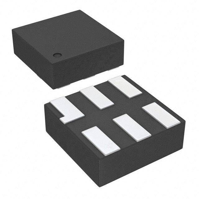
PIN CONFIGURATION
DSF PACKAGE
1-mm × 1-mm × 0.35-mm QFN-6
(TOP VIEW)
IN
1
6
ISF
GND
2
5
VCC
OUT
3
4
IDRV
PIN ASSIGNMENTS
PIN NAME
PIN NUMBER
TYPE
IN
1
Analog input
VEE
2
Ground
DESCRIPTION
Input terminal; connect this pin to the sensor output
Negative supply terminal; must be connected to ground
OUT
3
Analog output
IDRV
4
Analog input
VCC
5
Power
ISF
6
Analog input
Output terminal; connect this pin to the AFE input
Drive current adjustment; refer to the application diagram for further details
Positive supply terminal; must be decoupled to the VEE terminal with a 0.1-µF
capacitor
Sink current adjustment; refer to the application diagram for further details
FUNCTIONAL BLOCK DIAGRAM
IN
1
IIN
ICC
GND
6
ISF
5
VCC
4
IDRV
IISF
2
IIDRV
OUT
3
Figure 1. Block Diagram
4
Submit Documentation Feedback
Copyright © 2011, Texas Instruments Incorporated
Product Folder Link(s): VSP1000
�VSP1000
SBES023A – SEPTEMBER 2011 – REVISED OCTOBER 2011
www.ti.com
TYPICAL CHARACTERISTICS
At TA = +25°C, VCC = 13 V, RIDRV = 90 kΩ, RISF = 300 kΩ, and CLOAD = 22 pF, unless otherwise noted.
BANDWIDTH vs IDRV
INPUT MARGIN FROM VCC vs IDRV
300
4
Input Margin From VCC (V)
Bandwidth (MHz)
250
200
150
100
50
0
60
80
100
IDRV (µA)
120
3
2
1
0
140
50
100
150
IDRV (µA)
G001
Figure 2.
100
4
75
50
25
100
150
200
250
300
G006
INPUT LOAD CURRENT vs RISF
5
Input Load Current (mA)
IDRV Current (µA)
IDRV vs RIDRV
50
250
Figure 3.
125
0
200
350
400
450
IDRV Resistance (kΩ)
3
2
1
0
100 150 200 250 300 350 400 450 500 550 600 650
500
RISF (kΩ)
G002
Figure 4.
G004
Figure 5.
IDRV vs TEMPERATURE
INPUT LOAD CURRENT vs TEMPERATURE
80
3
Input Load Current (mA)
2.8
IDRV (µA)
75
70
65
2.6
2.4
2.2
2
1.8
1.6
1.4
1.2
60
−5
10
25
40
55
Temperature (°C)
70
85
1
0
G003
Figure 6.
12.5
25
37.5
50
Temperature (°C)
62.5
75
85
G005
Figure 7.
Submit Documentation Feedback
Copyright © 2011, Texas Instruments Incorporated
Product Folder Link(s): VSP1000
5
�VSP1000
SBES023A – SEPTEMBER 2011 – REVISED OCTOBER 2011
www.ti.com
TYPICAL CHARACTERISTICS (continued)
At TA = +25°C, VCC = 13 V, RIDRV = 90 kΩ, RISF = 300 kΩ, and CLOAD = 22 pF, unless otherwise noted.
ICC vs TEMPERATURE
3
ICC (mA)
2.5
2
1.5
1
0
12.5
25
37.5
50
Temperature (°C)
62.5
75
85
G007
Figure 8.
OVERVIEW
TYPICAL APPLICATION CIRCUIT
Figure 9 shows a typical application circuit for the VSP1000.
VCC
0.1 mF
C4
RISF
6
ISF
5
4
VCC
IDRV
RIDRV
Device
IN
1
GND
OUT
2
3
To AFE
From CCD
Figure 9. Typical Application Circuit
6
Submit Documentation Feedback
Copyright © 2011, Texas Instruments Incorporated
Product Folder Link(s): VSP1000
�VSP1000
SBES023A – SEPTEMBER 2011 – REVISED OCTOBER 2011
www.ti.com
DESIGN EQUATIONS
The CCD outputs must be loaded with current for proper operation. The VSP1000 provides the ability to draw
adjustable current through the IN pin. The value of the input load current can be set by choosing an appropriate
value of RISF connected to the ISF pin, as per Equation 1.
(VCC ´ 100 kW)
(RISF + 100 kW)
IIN =
- 1.2
1 kW
(1)
The bandwidth of the VSP1000 can be adjusted using the IDRV pin. The resistor connected at IDRV determines
the drive strength of the output buffer as well as the total quiescent current of the VSP1000. Equation 2 and
Equation 3 describe the relationship between RIDRV and the drive strength. CIDRV is used to increase the
power-supply rejection ratio of the device. A value of 0.1 µF for CIDRV is recommended.
(VCC - 5)
IDRV =
(RIDRV + 10 kW)
(2)
ICC = 26 ´ IDRV
(3)
EXAMPLE CONFIGURATIONS
Table 1 details several example configurations for the VSP1000. All examples are with VCC = 13 V.
Table 1. Example Configurations
CONFIGURATION
ICC (mA)
RISF (kΩ)
RIDRV (kΩ)
Bandwidth = 170 MHz , IIN = 2 mA
1.5
300
133
Bandwidth = 170 MHz , IIN = 4 mA
1.5
150
133
Bandwidth = 210 MHz , IIN = 2 mA
2
300
91
Bandwidth = 210 MHz , IIN = 4 mA
2
150
91
Bandwidth = 260 MHz , IIN = 2 mA
3
300
62
Bandwidth = 260 MHz , IIN = 4 mA
3
150
62
LAYOUT GUIDELINES
The decoupling capacitors CIDRV, RIDRV, and RISF should be placed as close as possible to the VSP1000.
Submit Documentation Feedback
Copyright © 2011, Texas Instruments Incorporated
Product Folder Link(s): VSP1000
7
�VSP1000
SBES023A – SEPTEMBER 2011 – REVISED OCTOBER 2011
www.ti.com
REVISION HISTORY
NOTE: Page numbers for previous revisions may differ from page numbers in the current version.
Changes from Original (September 2011) to Revision A
Page
•
Updated Figure 4 .................................................................................................................................................................. 5
•
Updated Figure 5 .................................................................................................................................................................. 5
8
Submit Documentation Feedback
Copyright © 2011, Texas Instruments Incorporated
Product Folder Link(s): VSP1000
�PACKAGE OPTION ADDENDUM
www.ti.com
10-Dec-2020
PACKAGING INFORMATION
Orderable Device
Status
(1)
Package Type Package Pins Package
Drawing
Qty
Eco Plan
(2)
Lead finish/
Ball material
MSL Peak Temp
Op Temp (°C)
Device Marking
(3)
(4/5)
(6)
VSP1000DSFR
ACTIVE
SON
DSF
6
5000
RoHS & Green NIPDAU | NIPDAUAG
Level-1-260C-UNLIM
0 to 85
VK
VSP1000DSFT
ACTIVE
SON
DSF
6
250
RoHS & Green NIPDAU | NIPDAUAG
Level-1-260C-UNLIM
0 to 85
VK
(1)
The marketing status values are defined as follows:
ACTIVE: Product device recommended for new designs.
LIFEBUY: TI has announced that the device will be discontinued, and a lifetime-buy period is in effect.
NRND: Not recommended for new designs. Device is in production to support existing customers, but TI does not recommend using this part in a new design.
PREVIEW: Device has been announced but is not in production. Samples may or may not be available.
OBSOLETE: TI has discontinued the production of the device.
(2)
RoHS: TI defines "RoHS" to mean semiconductor products that are compliant with the current EU RoHS requirements for all 10 RoHS substances, including the requirement that RoHS substance
do not exceed 0.1% by weight in homogeneous materials. Where designed to be soldered at high temperatures, "RoHS" products are suitable for use in specified lead-free processes. TI may
reference these types of products as "Pb-Free".
RoHS Exempt: TI defines "RoHS Exempt" to mean products that contain lead but are compliant with EU RoHS pursuant to a specific EU RoHS exemption.
Green: TI defines "Green" to mean the content of Chlorine (Cl) and Bromine (Br) based flame retardants meet JS709B low halogen requirements of


 工商网监
湘ICP备2023018690号
工商网监
湘ICP备2023018690号

