VS
VSP2582
P2
582
www.ti.com
SBES002B – JUNE 2008 – REVISED JUNE 2011
CCD ANALOG FRONT-END FOR DIGITAL CAMERAS
Check for Samples: VSP2582
FEATURES
DESCRIPTION
•
The VSP2582 is a complete mixed-signal processing
IC for digital cameras that provides correlated double
sampling (CDS) and analog-to-digital conversion
(ADC) for the output of charge-coupled device (CCD)
array. The CDS extracts video information of the
pixels from the CCD signal, and the ADC converts it
to a digital signal. For varying illumination conditions,
–9 dB to +35 dB very stable gain control is provided.
This gain control is linear in dB. Input signal clamping
and offset correction of the input CDS are also
provided.
1
2
•
•
•
•
•
•
CCD Signal Processing:
– 36-MHz Correlated Double Sampling (CDS)
12-Bit Analog-to-Digital Conversion:
– 36-MHz Conversion Rate
– No Missing Codes Ensured
78-dB Input-referred SNR (at CDS Gain 0 dB)
Programmable Black Level Clamping
Programmable Gain Amp (PGA):
–9 dB to +35 dB, –3 dB to +9 dB
by Analog Front Gain (CDS)
–6 dB to +26 dB by Digital Gain
Portable Operation:
– Low Voltage: 2.7 V to 3.6 V
– Low Power: 85 mW at 3.0 V and 36 MHz,
1 mW in Standby Mode
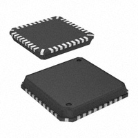
QFN-36 Package
Offset correction is performed by an Optical Black
(OB) level calibration loop, and held at a calibrated
black level clamping for an accurate black level
reference. Additionally, the black level is quickly
recovered after a gain change.
The VSP2582 is available in a QFN-36 package, and
operates from a single +3 V supply. The RHH
package features an exposed thermal pad, resulting
in substantially improved thermal performance.
1
2
Please be aware that an important notice concerning availability, standard warranty, and use in critical applications of
Texas Instruments semiconductor products and disclaimers thereto appears at the end of this data sheet.
All trademarks are the property of their respective owners.
PRODUCTION DATA information is current as of publication date.
Products conform to specifications per the terms of the Texas
Instruments standard warranty. Production processing does not
necessarily include testing of all parameters.
Copyright © 2008–2011, Texas Instruments Incorporated
�VSP2582
SBES002B – JUNE 2008 – REVISED JUNE 2011
www.ti.com
This integrated circuit can be damaged by ESD. Texas Instruments recommends that all integrated circuits be handled with
appropriate precautions. Failure to observe proper handling and installation procedures can cause damage.
ESD damage can range from subtle performance degradation to complete device failure. Precision integrated circuits may be more
susceptible to damage because very small parametric changes could cause the device not to meet its published specifications.
PACKAGE/ORDERING INFORMATION (1)
PRODUCT
PACKAGELEAD
PACKAGE
DESIGNATOR
SPECIFIED
TEMPERATURE
RANGE
PACKAGE
MARKING
VSP2582RHN
QFN-36
RHN
–25°C to +85°C
VSP2582
VSP2582RHH
QFN-36
RHH
–25°C to +85°C
VSP2582
(1)
ORDERING
NUMBER
TRANSPORT
MEDIA, QUANTITY
VSP2582RHN
Tray, 250
VSP2582RHNR
Tape and Reel, 2000
VSP2582RHH
Tray, 490
VSP2582RHHR
Tape and Reel, 2500
For the most current package and ordering information see the Package Option Addendum at the end of this document, or see the TI
web site at www.ti.com.
ABSOLUTE MAXIMUM RATINGS (1)
Over operating free-air temperature range (unless otherwise noted).
PARAMETER
VSP2582
UNIT
+4.0
V
±0.1
V
Digital input voltage
–0.3 to (VDD + 0.3)
V
Analog input voltage
–0.3 to (VCC + 0.3)
V
±10
mA
Ambient temperature under bias
–25 to +85
°C
Storage temperature
–55 to +125
°C
Junction temperature
+150
°C
Package temperature (reflow, peak)
+250
°C
Supply voltage
VCC, VDD
Ground voltage differences: AGND, DGND
Input current (any pins except supplies)
(1)
Stresses beyond those listed under absolute maximum ratings may cause permanent damage to the device. Exposure to absolutemaximum-rated conditions for extended periods may affect device reliability. These are stress ratings only and functional operation of
the device at these or any other conditions beyond those indicated under recommended operating conditions is not implied.
RECOMMENDED OPERATING CONDITIONS
Over operating free-air temperature range (unless otherwise noted).
MIN
NOM
MAX
UNIT
Analog supply voltage
VCC
2.7
3.0
3.6
V
Digital supply voltage
VDD
2.7
3.0
3.6
V
MCK
12
36
MHz
20
MHz
20
pF
+85
°C
Digital input logic family
Digital input clock frequency
CMOS
SCLK
Digital output load capacitance
Operating free-air temperature, TA
2
–25
Submit Documentation Feedback
Copyright © 2008–2011, Texas Instruments Incorporated
Product Folder Links: VSP2582
�VSP2582
www.ti.com
SBES002B – JUNE 2008 – REVISED JUNE 2011
ELECTRICAL CHARACTERISTICS
Over operating free-air temperature range (unless otherwise noted).
VSP2582RHN
PARAMETER
TEST CONDITIONS
MIN
Resolution
TYP
MAX
UNIT
36
MHz
12
Conversion rate
Bits
ANALOG INPUT (CCDIN)
Input signal level for full-scale out
CDS gain = 0 dB, DPGA gain = 0 dB
1000
mV
Maximum input range
CDS gain = –3 dB, DPGA gain = 0 dB
1300
mV
Input capacitance
15
Input limit
–0.3
pF
3.3
V
TRANSFER CHARACTERISTICS
Differential nonlinearity (DNL)
CDS gain = 0 dB, DPGA gain = 0 dB
Integral nonlinearity (INL)
CDS gain = 0 dB, DPGA gain = 0 dB
No missing codes
±2
LSB
Full-scale step input
1
Pixel
Step input from 1.8 V to 0 V
2
Pixels
6
Clock
Grounded input cap, PGA gain = 0 dB
78
dB
Grounded input cap, CDS gain = +9 dB
71
dB
Data latency
Signal-to-noise ratio (1)
LSB
Ensured
Step response settling time
Overload recovery time
±0.5
CCD offset correction range
–200
200
mV
INPUT CLAMP
Clamp-on resistance
400
Ω
Clamp level
1.5
V
PROGRAMMABLE ANALOG FRONT GAIN (CDS)
Minimum gain
Gain code = 111
–3
dB
Default gain
Gain code = 000
0
dB
Medium gain 1
Gain code = 001
3
dB
Medium gain 2
Gain code = 010
6
dB
Maximum gain
Gain code = 011
9
dB
0.5
dB
Gain control error
PROGRAMMABLE DIGITAL GAIN (DPGA)
Programmable gain range
–6
Gain step
26
dB
0.03125
dB
10
Bits
40.7
μs
OPTICAL BLACK CLAMP LOOP
Control DAC resolution
Loop time constant
OB loop IDAC × 1, CCOB = 0.1 μF
Programmable range of clamp level
Optical black clamp level
(1)
64
312
LSB
OBCLP level at CODE = 0 1000
128
LSB
OB level program step
8
LSB
Input-referred; SNR = 20 log (full-scale voltage/rms noise).
Submit Documentation Feedback
Copyright © 2008–2011, Texas Instruments Incorporated
Product Folder Links: VSP2582
3
�VSP2582
SBES002B – JUNE 2008 – REVISED JUNE 2011
www.ti.com
ELECTRICAL CHARACTERISTICS (continued)
Over operating free-air temperature range (unless otherwise noted).
VSP2582RHN
PARAMETER
TEST CONDITIONS
MIN
TYP
MAX
UNIT
DIGITAL INPUTS
Logic family
CMOS
Input voltage
Input current
VT+
LOW to HIGH threshold voltage
1.7
VT–
HIGH to LOW threshold voltage
1.0
V
V
IIH
Logic HIGH, VIN = +3 V
±20
μA
IIL
Logic LOW, VIN = 0 V
±20
μA
VCC +
0.3
V
Input capacitance
5
Maximum input voltage
–0.3
DIGITAL OUTPUTS (DATA)
Logic family
CMOS
Logic coding
Straight Binary
VOH
Output voltage
2.4
V
VOL
0.4
Additional data output delay
V
Output data delay code = 00
0
ns
Output data delay code = 01
2
ns
Output data delay code = 10
4
ns
Output data delay code = 11
6
ns
POWER SUPPLY
VCC
Supply voltage
VDD
Power dissipation
Standby mode power dissipation
2.7
3.0
3.6
2.7
3.0
3.6
V
V
at 3.0 V 36 MHz
85
mW
Clocks (SHP/SHD/ADCCK) off mode
(at 3.0 V)
1
mW
TEMPERATURE RANGE
Operation temperature
–25
+85
°C
THERMAL INFORMATION
VSP2582RHH
THERMAL METRIC (1)
VSP2582RHNR
RHH
RHN
36 PINS
36 PINS
θJA
Junction-to-ambient thermal resistance
31.7
81.0
θJCtop
Junction-to-case (top) thermal resistance
19.3
22.7
θJB
Junction-to-board thermal resistance
6.7
45.6
ψJT
Junction-to-top characterization parameter
0.3
0.8
ψJB
Junction-to-board characterization parameter
6.7
44.9
θJCbot
Junction-to-case (bottom) thermal resistance
1.5
n/a
(1)
4
UNITS
°C/W
For more information about traditional and new thermal metrics, see the IC Package Thermal Metrics application report, SPRA953.
Submit Documentation Feedback
Copyright © 2008–2011, Texas Instruments Incorporated
Product Folder Links: VSP2582
�VSP2582
www.ti.com
SBES002B – JUNE 2008 – REVISED JUNE 2011
PIN CONFIGURATION
COB
BYPP
BYP
CCDIN
AGND
AGND
VCC
VCC
AGND
RHH AND RHN PACKAGES
QFN-36
(TOP VIEW)
27
26
25
24
23
22
21
20
19
VCC
30
16
CLPOB
AGND
31
15
CLPDM
SLOAD
32
14
VCC
SDATA
33
13
ADCCK
SCLK
34
12
DGND
B0 (LSB)
35
11
VDD
B1
36
10
B11 (MSB)
2
3
4
5
6
7
8
9
B10
1
B9
SHP
B8
17
B7
29
B6
REFP
B5
SHD
B4
18
B3
28
B2
REFN
Table 1. TERMINAL FUNCTIONS
TERMINAL
(1)
NAME
NO.
TYPE (1)
B2
1
DO
Data out bit 2
B3
2
DO
Data out bit 3
B4
3
DO
Data out bit 4
B5
4
DO
Data out bit 5
B6
5
DO
Data out bit 6
B7
6
DO
Data out bit 7
B8
7
DO
Data out bit 8
B9
8
DO
Data out bit 9
B10
9
DO
Data out bit 10
B11
10
DO
Data out bit 11 (MSB)
VDD
11
P
Digital power supply for data output
DGND
12
P
Digital ground for data output
ADCCK
13
DI
Clock for digital output buffer
VCC
14
P
Analog power supply
CLPDM
15
DI
CLPDM signal
CLPOB
16
DI
CLPOB signal
Sampling clock for reference level of CCD signal
DESCRIPTION
SHP
17
DI
SHD
18
DI
Sampling clock for data level of CCD signal
AGND
19
P
Analog ground
VCC
20
P
Analog power supply
VCC
21
P
Analog power supply
Designators in TYPE: P: Power Supply and Ground, DI: Digital Input, DO: Digital Output, AI: Analog Input, AO: Analog Output.
Submit Documentation Feedback
Copyright © 2008–2011, Texas Instruments Incorporated
Product Folder Links: VSP2582
5
�VSP2582
SBES002B – JUNE 2008 – REVISED JUNE 2011
www.ti.com
Table 1. TERMINAL FUNCTIONS (continued)
TERMINAL
NAME
NO.
TYPE (1)
DESCRIPTION
AGND
22
P
Analog ground
AGND
23
P
Analog ground
CCDIN
24
AI
CCD signal input
BYP
25
AO
Internal reference bypass to ground by 0.1 μF
BYPP
26
AO
Internal reference bypass to ground by 1000 pF
COB
27
AO
OB loop feed back capacitor
REFN
28
AO
Internal reference bypass to ground by 0.1 μF
REFP
29
AO
Internal reference bypass to ground by 0.1 μF
VCC
30
P
Analog power supply
AGND
31
P
Analog ground
SLOAD
32
DI
Serial data latch signal
SDATA
33
DI
Serial data input
SCLK
34
DI
Serial data clock
B0
35
DO
Data out bit 0 (LSB)
B1
36
DO
Data out bit 1
FUNCTIONAL BLOCK DIAGRAM
BYPP
COP
BYP
REFP
REFN
Internal Reference
CCD
Output
Signal
Buff
CDS
CCDIN
Clamp
Gain Setting
CDS
Decoder
Digital
Output
12-Bit
DPGA
and
Output Register
16-Bit
Analog-to-Digital
Converter
SHP/SHD
ADCCK
ADCCK
Internal
Timing
Circuit
CLPDM
SHD
CLPDM
CLPOB
Serial Interface
and
Register
6
SHP
Submit Documentation Feedback
SDATA
SCLK
SLOAD
Copyright © 2008–2011, Texas Instruments Incorporated
Product Folder Links: VSP2582
�VSP2582
www.ti.com
SBES002B – JUNE 2008 – REVISED JUNE 2011
TIMING SPECIFICATIONS
CCD
N
N+1
N+2
N+3
tWP
SHP
tPD
tWD
tS
tWD
SHD
tINHIBIT2
tS
tCKP
tADC
tADC
tINHIBIT1
ADCCK
tOD
B0-B9
N-6
N-5
N-4
N-3
Figure 1. TG High-Speed Pulse Specifications
TIMING CHARACTERISTICS (36-MHz Operation)
SYMBOL
PARAMETER
MIN
tCKP
Clock period
27.7
TYP
MAX
tADC
ADCCK high or low level
tWP
UNIT
6.5
13.8
21.2
SHP pulse width
5.9
6.9
ns
tWD
SHD pulse width
5.9
6.9
ns
tPD
SHP trailing edge to SHD leading edge
5.0
6.9
ns
tDP
SHD trailing edge to SHP leading edge
5.2
6.9
ns
3
ns
ns
ns
tS
Sampling delay
tINHIBIT1
Inhibited clock period 1 (from rising edge of SHP to rising
edge of ADCCK)
–9
13
ns
tINHIBIT2
Inhibited clock period 2 (from rising edge of SHD to rising
edge of ADCCK)
–8
–0
ns
tOD
Output delay
0
DL
Data latency
5
6
ns
Clocks
TIMING CHARACTERISTICS (27-MHz Operation)
SYMBOL
PARAMETER
MIN
TYP
MAX
37
UNIT
tCKP
Clock period
tADC
ADCCK high or low level
6.5
18.5
ns
tWP
SHP pulse width
5.9
6.9
ns
tWD
SHD pulse width
5.9
6.9
ns
tPD
SHP trailing edge to SHD leading edge
5.9
6.9
ns
tDP
SHD trailing edge to SHP leading edge
5.2
6.9
ns
tS
Sampling delay
3
ns
tINHIBIT1
Inhibited clock period 1 (from rising edge of SHP to rising
edge of ADCCK)
–9
13
ns
tINHIBIT2
Inhibited clock period 2 (from rising edge of SHD to rising
edge of ADCCK)
–8
–0
ns
tOD
Output delay
0
DL
Data latency
30.5
5
6
ns
ns
Clocks
Submit Documentation Feedback
Copyright © 2008–2011, Texas Instruments Incorporated
Product Folder Links: VSP2582
7
�VSP2582
SBES002B – JUNE 2008 – REVISED JUNE 2011
www.ti.com
tINHIBIT1
27.77ns
SHP
ADCCK
(rise)
tINHIBIT1
tINHIBIT1
tINHIBIT1
tINHIBIT1
9ns
ADCCK
13ns
Note that in condition of OD (Output delay) = 00
tINHIBIT2
27.77ns
SHP
ADCCK
(rise)
tINHIBIT2
tINHIBIT2
tINHIBIT2
tINHIBIT2
8ns
ADCCK
0ns
Figure 2. TG High-Speed Pulse Specifications (Detail of inhibit area)
8
Submit Documentation Feedback
Copyright © 2008–2011, Texas Instruments Incorporated
Product Folder Links: VSP2582
�VSP2582
www.ti.com
SBES002B – JUNE 2008 – REVISED JUNE 2011
SLOAD
tXH
tXS
tCKL
tCKP
tCKHX
tCKH
SCLK
tDH
tDS
SDATA
LSB
A0
A1
A2
MSB
D5
D4
2 Bytes
Figure 3. Serial Interface Timing Specification
SYMBOL
PARAMETER
MIN
tCKP
Clock period
50
TYP
MAX
UNIT
ns
tCHH
Clock high pulse width
25
ns
tCHL
Clock low pulse width
25
ns
tDS
Data setup time
15
ns
tDH
Data hold time
15
ns
tXS
SLOAD to SCLK setup time
20
ns
tXH
SCLK to SLOAD hold time
20
ns
tCKHX
SCLK hold time of final SCLK
0
ns
Submit Documentation Feedback
Copyright © 2008–2011, Texas Instruments Incorporated
Product Folder Links: VSP2582
9
�VSP2582
SBES002B – JUNE 2008 – REVISED JUNE 2011
www.ti.com
APPLICATION INFORMATION
Overview
The VSP2582 is a complete mixed-signal IC that contains all of the key features associated with processing the
CCD imager output signal in a video camera, digital still camera, security camera, or similar application. A
simplified block diagram is shown in Figure 4. The VSP2582 includes a correlated double sampler (CDS), a
programmable gain amplifier (PGA), an analog-to-digital converter (ADC), an input clamp, an optical black (OB)
level clamp loop, a serial interface, timing control, and a reference voltage generator. All functions and
parameters such as PGA gain control, operating mode, and other settings are controlled by the serial interface.
BYPP
COP
From Serial Interface
Current
DAC
Buff
Decorder
Gain Control
16-Bit
ADC
CDS
CCDIN
Digital
Output
12-Bit
DPGA
Clamp
Internal Clocks (SHP/SHD ADCCK, CLPOB, CLPDM)
From Internal
Timing Circuit
Figure 4. Simplified Block Diagram of VSP2582
Correlated Double Sampler (CDS)
The output signal of a CCD image sensor is sampled twice during one pixel period: once at the reference interval
and again at the data interval. Subtracting these two samples extracts the video information of the pixel as well
as removes any noise which is common (or correlated) to both intervals. CDS is critical to reduce the reset noise
and the low-frequency noise that is present on the CCD output signal. Figure 5 shows the block diagram of the
CDS.
SHD
SHP/SHD
CINP
C1
CCDIN
CCD
Output
SHP
C2
CLPDM
REFP
SHD
SHP
Figure 5. Block Diagram of CDS and Input Clamp
10
Submit Documentation Feedback
Copyright © 2008–2011, Texas Instruments Incorporated
Product Folder Links: VSP2582
�VSP2582
www.ti.com
SBES002B – JUNE 2008 – REVISED JUNE 2011
Input Clamp
The buffered CCD output is capacitively coupled to the VSP2582. The purpose of the input clamp is to restore
the dc component of the input signal that was lost with ac coupling and establish the desired dc bias point for the
CDS. Figure 5 also shows the block diagram of the input clamp. The input level is clamped to the internal
reference voltage REFP (1.5 V) during the dummy pixel interval. More specifically, the clamping function
becomes active when both CLPDM and SHP are active. Immediately after power ON, the clamp voltage of input
capacitor has not charged. The VSP2582 provides a boost-up circuit for fast charging of the clamp voltage.
16-Bit A/D Converter
The VSP2582 includes a high-speed, 16-bit ADC. This ADC uses a fully differential pipelined architecture with
correction. The ADC architecture correction is very advantageous to achieve better linearity for a smaller signal
level because large linearity errors tend to occur at specific points in the full scale; linearity improves for a level of
signal below that specific point. The ADC ensures 16-bit resolution across the entire full-scale range.
Optical Black (OB) Level Loop and OB Clamp Level
The VSP2582 has a built-in OB offset self calibration circuit (OB loop) that compensates the OB level by using
Optical Black (OB) pixels output from the CCD image sensor. A block diagram of the OB loop and the OB clamp
circuit is shown in Figure 6. The CCD offset is compensated by this calibration circuit while activating CLPOB
during a period when OB pixels are output from the CCD.
OB Clamp
Level
CCDIN
16-Bit
ADC
CDS
DATA
OUT
DPGA
BYPP
Current
DAC
COB
Decoder
CPLOB
Figure 6. OB Loop and OB Level Clamp
Submit Documentation Feedback
Copyright © 2008–2011, Texas Instruments Incorporated
Product Folder Links: VSP2582
11
�VSP2582
SBES002B – JUNE 2008 – REVISED JUNE 2011
www.ti.com
At the CDS circuit, the CCD offset is compensated as a difference between the reference level and the data level
of the OB pixel. The compensated signal levels are recognized as actual OB levels, and outputs are clamped to
OB levels set by the serial interface. These OB levels are the base of black for the effective pixel period
thereafter.
Since the DPGA is a gain stage outside the OB loop, OB levels are not affected even when the gain changes.
The converging time of the OB loop is determined based on the capacitor value connected to the COB terminal
and the output from the current output data-to-analog converter (DAC) of the loop. The time constant can be
obtained from following equation:
xxx
T = C/(16384 ´ IMIN)
(1)
Where C is the capacitor value connected to COB, and IMIN is minimum current (0.15 μA) of the current DAC.
which is a current equivalent to 1 LSB of the DAC output. When C = 0.1 μF, T will be 40.7 μs. The slew rate, SR,
can be obtained from following equation:
xxx
SR = IMAX/C
(2)
Where, C is the capacitor value connected to COB, and IMAX is maximum current (153 μA) of the current DAC,
with a current equivalent to 1023 LSB of the DAC output.
DAC output current multiplication is provided. This function increases the DAC output current through the serial
interface at x2, x4 and x8. Increased DAC current shortens the time constant of the OB loop. This function is
effective when a particular OB level changes significantly and requires fast loop setting.
On device power up, the COB capacitor voltages have not charged. For fast start up, a COB voltage boost-up
circuit is provided.
The OB clamp level (digital output value) can be set from an external source through the serial interface by
inputting a digital code to the OB clamp level register. The digital code to be input and the corresponding OB
clamp level are shown in Table 2.
Table 2. Input Code and OB Clamp Level to be Set
CLAMP LEVEL
12
CODE
VSP2582 (12-BIT)
0 0000 (default)
64 LSB
0 0001
72 LSB
:
:
0 0110
112 LSB
0 0111
120 LSB
0 1000 (default)
128 LSB
0 1001
136 LSB
:
:
1 1110
304 LSB
1 1111
312 LSB
Submit Documentation Feedback
Copyright © 2008–2011, Texas Instruments Incorporated
Product Folder Links: VSP2582
�VSP2582
www.ti.com
SBES002B – JUNE 2008 – REVISED JUNE 2011
Programmable Gain
The VSP2582 has a wide programmable gain range of –9 dB to 35 dB. The desired gain is set as a combination
of the CDS gain and Digital Programmable Gain Amplifier (DPGA). The CDS gain can be programmed over the
range of –3 dB to 9 dB in 3-dB steps. Digital gain can be programmed from –6 dB to 26 dB by a 0.03125 dB
step. Both gain settings are controlled through the serial interface. Digital Gain changes linearly in proportion to
the setting code. Figure 7 shows the relationship of input code and digital gain.
The recommend usage of the CDS and digital gain combination is to first adjust the CDS gain as a primary
image signal amplification; then, use digital gain as an adaptive gain control. The wide range of Digital gain
covers the necessary gain range on most applications; if necessary, the CDS gain should be changed at periods
that do not affect a picture such as a blanking period.
30
25
Gain (dB)
20
15
10
5
0
-5
-10
0
128
256
384
512
640
768
896
1024
Input Code for Gain Control (0 to 1023)
Figure 7. Setting Code vs. Digital Gain
Standby Mode and Power Trim Function
For the purposes of power saving, the VSP2582 can be put into a Standby Mode by the serial interface control
when the device is not in use. In this mode, all functional blocks are disabled and the digital outputs all go to
zero. Current consumption drops to approximately 2 mA. Only 10 ms are required to restore activity from the
Standby Mode. Enter and resume from the Standby Mode through the serial interface.
The VSP2582 also provides a power trim function. This function trims the power of the CDS, ADC and Reference
source. Through this trim function, power consumption can be reduced, although this reduction is not
recommended at 36-MHz operation because accuracy may degrade. This function is useful for low sampling rate
operation.
Timings
The CDS and the ADC are operated by SHP and SHD; the respective derivative timing clocks are generated by
the on-chip timing generator. The Output Register and Decoder are operated by ADCCK. The digital output data
are synchronized with ADCCK. The timing relationship between the CCD signal, SHP, SHD, ADCCK, and the
output data is shown in Figure 1. CLPOB activates the black level clamp loop during the OB pixel interval and
CLPDM activates the input clamping during the dummy pixel interval. In the Standby mode, all of ADCCK, SHP,
SHD, CLPOB and CLPDM data are internally masked and pulled HIGH.
As explained in the Input Clamp and Optical Black Level (OB) Loop and OB Clamp Level sections, CLPOB is
used to control the OB loop which compensates CCD offset automatically. CLPDM is used to charge the input
clamp voltage to capacitor CIN which is connected to CCDIN. For proper operation, both CLPOB and CLPDM
should be activated in the following manner.
Submit Documentation Feedback
Copyright © 2008–2011, Texas Instruments Incorporated
Product Folder Links: VSP2582
13
�VSP2582
SBES002B – JUNE 2008 – REVISED JUNE 2011
www.ti.com
The CCD has several dummy and Optical Black pixels per line. The placement of these pixels depends on the
CCD manufacturer, but are usually at the beginning and end of the line with the imaging pixels in between.
During the time the dummy pixels are being read from the CCD, it is recommended to activate CLPDM. During
the time the Optical Black pixels are being read, it is recommended to activate CLPOB. If there are only a few
dummy pixels, then the leakage from capacitor CIN may become excessive. In this case, extend the active period
of CLPDM into the Optical Black pixels. Do not activate CLPDM and CLPOB at the same time; each of these
pixel types must be used only as either a dummy pixel (CLPDM active) or an Optical Black pixel (CLPOB active).
Typically for CLPOB about 20 pixels per line are sufficient and for CLPDM about CLPDM about 10-20 pixels are
sufficient. Figure 8 shows typical timing for CLPDM and CLPOB for a line of CCD readout.
Under default conditions, SHP and SHD are active on the rising edge; CLPOB and CLPDM are active low. The
active state of each signal can be selected by register settings.
SHP, SHD, CLPOB, and CLPDM are active at low periods or upon a rising edge at the default setting of the
serial interface; each active polarity can be selected by a register setting.
1H
CCD
OUTPUT
OB
DM
Pixel
Image Pixel
Image Pixel
OB Pixel
CLPOB
CLPDM
Figure 8. Timing for CLPOB and CLPDM
Voltage Reference
All reference voltages and bias currents used on the device are created from an internal bandgap circuitry. The
VSP2582 has symmetrical independent voltage reference for each channel.
Both channels of CDS and the ADC use three primary reference voltages. REFP (1.5 V) and REFN (1.0 V) are
individual references. REFP and REFN are buffered on-chip. The ADC full-scale range is determined by twice
the difference voltage between REFP and REFN.
REFP and REFN should be heavily decoupled with appropriate capacitors.
Hot Pixel Rejection
Sometimes an OB pixel output signal from the CCD includes unusual signal levels that are caused by pixel
defection. If this level reaches full-scale level, it may affect OB level stability. The VSP2582 is able to reject an
unusually large pixel level (hot pixel) at the OB pixel. This function may contribute to CCD yield improvement
which is caused by OB pixel failure.
The rejection level for hot pixels is able to programmed through the serial interface. When the OB pixel level
exceeds that level, the VSP2582 omits it and uses the previous pixel level for OB level calculation.
14
Submit Documentation Feedback
Copyright © 2008–2011, Texas Instruments Incorporated
Product Folder Links: VSP2582
�VSP2582
www.ti.com
SBES002B – JUNE 2008 – REVISED JUNE 2011
SERIAL INTERFACE
All functions and settings of the VSP2582 are controlled through the serial interface. The VSP2582 serial
interface is composed of three signals: SDATA, SCLK, and SLOAD. SDATA data are sequentially stored to shift
into the register at a rising edge or SCLK, and shift register data are stored in a parallel latch at an SLOAD rising
edge. Before a write operation, SLOAD must go LOW and stay low during the write process. (Refer serial
interface timing description)
The serial interface command is composed of a 10-bit address and 6 bits of data. The fundamental write
operation is done in a 2-byte write mode. In this mode, one serial interface command is sent by one combination
of address and data bits. The 10 address bits should be sent LSB first, followed by 6 bits of data also sent LSB
first. The 6-bit command data are stored to the respective register by the 10 address bits at the rising edge of
SLOAD. The stored serial command data takes effect immediately upon the rising edge of SLOAD.
The VSP2582 also supports a continuous write mode as below. When the input serial data are longer than 2
bytes (16 bits), the following data stream is automatically recognized as the data of next address. In this mode, 6
bits of serial command data are stored to the respective register immediately when those data are fetched.
Address and data should be sent LSB first, the same as the 2-byte writing mode. If a data bit is not complete, or
if there are 6 bits at the end part of this data stream, non fill-up data bits are ignored.
The setting for the serial interface register is described in the Serial Interface Register Description. Figure 9
shows the continuous writing mode.
SLOAD
SCLK
SDATA
A0
A9
D0
10-Bit
Address
D5
D0
6-Bit
Data (1)
D5
D0
6-Bit
Data (2)
D5
6-Bit
Data (3)
Figure 9. Continuous Writing Mode
Serial Interface Register Description
Table 3 shows the serial interface command data format. Descriptions of each register follow.
Table 3. Serial Interface Command Data Format
ADDRESS
DATA
MSB
LSB
MSB
LSB
REGISTERS
A9
A8
A7
A6
A5
A4
A3
A2
A1
A0
D5
D4
D3
D2
D1
D0
Clk-Pol-ctrl
0
0
0
0
0
0
0
0
0
0
D5
D4
D3
0
0
0
AFE-ctrl(1)
0
0
0
0
0
0
0
0
0
1
0
0
D3
0
0
D0
AFE-ctrl(2)
0
0
0
0
0
0
0
0
1
0
0
D4
0
0
D1
D0
S-delay
0
0
0
0
0
0
0
0
1
1
0
0
0
0
D1
D0
Clamp
0
0
0
0
0
0
0
1
0
0
0
D4
D3
D2
D1
D0
Hot-pixel
0
0
0
0
0
0
0
1
0
1
D5
D4
D3
D2
D1
D0
D-PGA_L
0
0
0
0
0
0
0
1
1
0
D5
D4
D3
D2
D1
D0
D-PGA_U
0
0
0
0
0
0
0
1
1
1
0
0
D3
D2
D1
D0
A-PGA
0
0
0
0
0
0
1
0
0
0
0
0
0
D2
D1
D0
Power
0
0
0
0
0
0
1
0
0
1
0
D4
D3
D2
D1
D0
Reserved
Other address is reserved.
Do not use
Submit Documentation Feedback
Copyright © 2008–2011, Texas Instruments Incorporated
Product Folder Links: VSP2582
15
�VSP2582
SBES002B – JUNE 2008 – REVISED JUNE 2011
www.ti.com
Clk-Pol-ctrl Register (Address: h000)
Clk-Pol-ctrl selects the active polarity of CLPDM, CLPOB, and SHP/SHD.
DATA BIT
NAME
D3
CLPDM Polarity
0 : Active Low
DESCRIPTION
1 : Active High
DEFAULT
0
D4
CLPOB Polarity
0 : Active Low
1 : Active High
0
D5
SHP/SHD Polarity
0 : Active Low
1 : Active High
0
AFE-ctrl(1) Register (Address: h001)
DATA BIT
NAME
DESCRIPTION
DEFAULT
D0
Standby
0: Normal operation
1: standby
0
D3
Test enable
0: disable
1: enable
0
AFE-ctrl(2) Register (Address: h002)
AFE-ctrl(2) register controls the following data output settings.
DATA BIT
NAME
DESCRIPTION
D[1:0]
Data output delay
00: 0 ns, 01: 2 ns, 10: 4 ns, 11: 6 ns
DEFAULT
D4
Output enable
0: enable
0
1: Hi-Z
0
S-delay Register (Address: h003)
S-delay register controls SHD sampling start time from the rising edge or SHP.
DATA BIT
NAME
DESCRIPTION
DEFAULT
D[1:0]
Sampling delay for SHD
00: 0 ns, 01: 2 ns (10, 11 are not allowed)
0
Clamp Register (Address: h004)
D4
D3
D2
D1
D0
CLAMP LEVEL (VSP2582)
0
0
0
0
0
64 LSB
0
0
0
0
1
72 LSB
:
:
0
0
1
1
1
120 LSB
0
1
0
0
0
128 LSB (default)
0
1
0
0
1
136 LSB
:
:
1
1
1
1
0
304 LSB
1
1
1
1
1
312 LSB
Hot-pixel Register (Address: h005)
16
DATA BIT
NAME
D[4:0]
Hot pixel rejection level
D5
Hot pixel rejection disable
DESCRIPTION
DEFAULT
Hot pixel rejection level is givens following
equation.
RL (LSB) = 16 • (d[4:0] + 1)
Where: RL is level difference from OB level.
0: disable
Submit Documentation Feedback
1: enable
11111
1
Copyright © 2008–2011, Texas Instruments Incorporated
Product Folder Links: VSP2582
�VSP2582
www.ti.com
SBES002B – JUNE 2008 – REVISED JUNE 2011
D-PGA Register (Address: h006 and h007)
D-PGA_U
D-PGA_L
D[3:0]
ANALOG GAIN
DEFAULT
Digital PGA gain is givens following equation.
Gain (dB) = (D-PGA • 0.03125 ) – 6
Where: D-PGA is decimal value of 10-bit data
which is combined D-PGA_U and D-PGA_L. DPGA_U is MSB side of D-PGA.
D[5:0]
D-PGA = 00 1100 000 = 0 dB
A-PGA Register (Address: h008)
CDS Gain control
D2
D1
D0
ANALOG GAIN
0
0
0
0 dB (default)
0
0
1
3 dB
0
1
0
6 dB
0
1
1
9 dB
1
1
1
–3 dB
NOTE
Other values of D[2:0] are not applicable.
Power Register (Address: h009)
DATA BIT
NAME
DESCRIPTION
DEFAULT
D[1:0]
OB loop IDAC output current
00: x1, 01: x2, 10: x4, 11: x8
00
D[2]
CDS Power Trim
0: Normal CDS Power, 1: Reduce CDS Power
0
D[3]
ADC Power Trim
0: Normal ADC Power, 1: Reduce ADC Power
0
D[4]
Ref Power Trim
0: Normal Ref Power, 1: Reduce Ref Power
0
POWER SUPPLY, GROUNDING AND DEVICE DECOUPLING RECOMMENDATIONS
The VSP2582 incorporates a high-precision, high-speed analog-to-digital converter and analog circuitry that is
vulnerable to any extraneous noise from the rails or elsewhere. For this reason, although the VSP2582 has
multiple supply pins, it should be treated as an analog component; all supply pins except for VDD should be
powered by only the analog supply of the system. This configuration ensures the most consistent results,
because digital power lines often carry high levels of wideband noise that would otherwise be coupled into the
device and degrade achievable performance.
Proper grounding, short lead length, and proper use of ground planes are also very important for high-frequency
designs. Multilayer printed circuit boards (PCBs) are recommended for best performance because they offer
distinct advantages such as minimizing ground impedance, separation of signal layers by ground layers, etc. It is
highly recommended that the analog and digital ground pins of the VSP2582 be joined together at the IC and be
connected only to the analog ground of the system. The driver stage of the digital outputs (B(9:0]) is supplied
through a dedicated supply pin (VDD) and should be separated from the other supply pins completely, or at least
with a ferrite bead. It is also recommended to keep the capacitive loading on the output data lines as low as
possible (typically less than 15 pF). Larger capacitive loads demand higher charging current as a result of surges
that can feed back into the analog portion of the VSP2582 and affect performance. If possible, external buffers or
latches should be used that provide the added benefit of isolating the VSP2582 from any digital noise activities
on the data lines. In addition, resistors in series with each data line may help minimize surge current.
Submit Documentation Feedback
Copyright © 2008–2011, Texas Instruments Incorporated
Product Folder Links: VSP2582
17
�VSP2582
SBES002B – JUNE 2008 – REVISED JUNE 2011
www.ti.com
Because of the high operating speed, the converter also generates high-frequency current transients and noises
that are fed back into the supply and reference lines. This interference requires the supply and reference pins to
be sufficiently bypassed. In most cases, a 0.1-μF ceramic-chip capacitor is adequate to decouple the reference
pins. Supply pins should be decoupled to the ground plane with a parallel combination of tantalum (1 μF to 22
μF) and ceramic (0.1 μF) capacitors. The effectiveness of the decoupling largely depends on the proximity to the
individual pin. VDD should be decoupled to the proximity of DGND. Special attention must be paid to the
bypassing of COB and BYPP because these capacitor values determine the important analog performance of the
device. Although the recommend capacitor values for COB and BYPP are 0.1 μF and 1000 pF, respectively, it is
better to adjust the capacitor for BYPP at the case.
18
Submit Documentation Feedback
Copyright © 2008–2011, Texas Instruments Incorporated
Product Folder Links: VSP2582
�VSP2582
www.ti.com
SBES002B – JUNE 2008 – REVISED JUNE 2011
REVISION HISTORY
NOTE: Page numbers for previous revisions may differ from page numbers in the current version.
Changes from Revision A (September 2008) to Revision B
Page
•
Added last sentence to Description section .......................................................................................................................... 1
•
Added quantity to transport media of VSP2582RHN product in Package/Ordering Information table ................................. 2
•
Added VSP2582RHH product to Package/Ordering Information table ................................................................................ 2
•
Added thermal information table ........................................................................................................................................... 3
•
Deleted Thermal Range, Thermal resistance parameters from Electrical Characteristics table .......................................... 4
•
Updated pin out drawing, added RHH package ................................................................................................................... 5
Submit Documentation Feedback
Copyright © 2008–2011, Texas Instruments Incorporated
Product Folder Links: VSP2582
19
�PACKAGE OPTION ADDENDUM
www.ti.com
10-Dec-2020
PACKAGING INFORMATION
Orderable Device
Status
(1)
Package Type Package Pins Package
Drawing
Qty
Eco Plan
(2)
Lead finish/
Ball material
MSL Peak Temp
Op Temp (°C)
Device Marking
(3)
(4/5)
(6)
VSP2582RHHR
ACTIVE
VQFN
RHH
36
2500
RoHS & Green
NIPDAU
Level-3-260C-168 HR
-25 to 85
VSP2582
VSP2582RHN
ACTIVE
VQFN
RHN
36
250
RoHS & Green
NIPDAU
Level-1-260C-UNLIM
-25 to 85
VSP2582
VSP2582RHNR
NRND
VQFN
RHN
36
2000
RoHS & Green
NIPDAU
Level-1-260C-UNLIM
-25 to 85
VSP2582
VSP2582RHNRG4
NRND
VQFN
RHN
36
2000
RoHS & Green
NIPDAU
Level-1-260C-UNLIM
-25 to 85
VSP2582
(1)
The marketing status values are defined as follows:
ACTIVE: Product device recommended for new designs.
LIFEBUY: TI has announced that the device will be discontinued, and a lifetime-buy period is in effect.
NRND: Not recommended for new designs. Device is in production to support existing customers, but TI does not recommend using this part in a new design.
PREVIEW: Device has been announced but is not in production. Samples may or may not be available.
OBSOLETE: TI has discontinued the production of the device.
(2)
RoHS: TI defines "RoHS" to mean semiconductor products that are compliant with the current EU RoHS requirements for all 10 RoHS substances, including the requirement that RoHS substance
do not exceed 0.1% by weight in homogeneous materials. Where designed to be soldered at high temperatures, "RoHS" products are suitable for use in specified lead-free processes. TI may
reference these types of products as "Pb-Free".
RoHS Exempt: TI defines "RoHS Exempt" to mean products that contain lead but are compliant with EU RoHS pursuant to a specific EU RoHS exemption.
Green: TI defines "Green" to mean the content of Chlorine (Cl) and Bromine (Br) based flame retardants meet JS709B low halogen requirements of


 工商网监
湘ICP备2023018690号
工商网监
湘ICP备2023018690号
