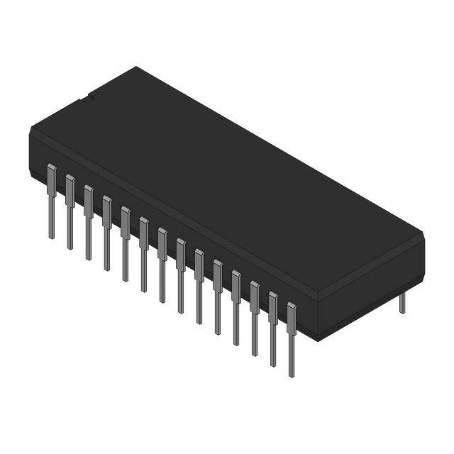
CS5321/22 24-bit, Variable-bandwidth A/D Converter Chipset
Features
CMOS A/D Converter Chipset Dynamic Range
- 130 dB @ 25 Hz Bandwidth - 121 dB @ 411 Hz Bandwidth
Description
The CS5321/CS5322 chipset functions as a unique A/D converter intended for very high-resolution measurement of signals below 1600 Hz. It is specifically designed for applications that require both a high dynamic range and a low total harmonic distortion. The chipset performs sampling, A/D conversion, and anti-alias filtering. The CS5321 uses Delta-Sigma modulation to produce highly accurate conversions. The ∆Σ modulator oversamples, virtually eliminating the need for external analog anti-alias filters. The CS5322 linear-phase FIR digital filter decimates the output to any one of seven selectable update periods: 16, 8, 4, 2, 1, 0.5, and 0.25 milliseconds. Data is output from the digital filter in a 24-bit serial format.
ORDERING INFORMATION
Delta-sigma Architecture
- Fourth-order Modulator - Variable Oversampling: 64X to 4096X - Internal Track-and-hold Amplifier
CS5321 Signal-to-distortion: 115 dB Clock-jitter-tolerant Architecture Input Voltage Range: +4.5 V Flexible Filter Chip
- Hardware- or Software-selectable Options - Seven Selectable Filter Corners (-3 dB) Frequencies: 25, 51, 102, 205, 411, 824 and 1650 Hz
Low Power Dissipation: (+VREF + 5%) ≈ (+VREF + 5%) +VREF 0V -VREF ≈ - (+VREF +5%) > - (+VREF +5%)
Error Flag Possible
Table 1. Output Coding for the CS5321 and CS5322 Combination
DS454F3
21
�CS5321/22
2.8 Performance
Figure 22, 23 and 24 illustrate the spectral performance of the CS5321/22 and chipset when operating from a 1.024 MHz master clock. Ten 1024 point FFTs were averaged to produce the plots. Figure 22 illustrates the chip set with a 100 Hz, -20 dB input signal. The sample rate was set at 1 kHz. Dynamic range is 122 dB. The dynamic range calculated by the test soft-ware is reduced somewhat in Figures 23 and 24 because of jitter in the signal test oscillator. Jitter in the 100 Hz signal source is interpreted by the signal processing software to be increased noise. The choice of master clock frequency will affect performance. The CS5321 will exhibit the best Signal to Distortion performance with slower modulator sampling clock rates as slower sample rates allow more time for amplifier settling. For lowest offset drift, the CS5321 should be operated with MCLK = 1.024 MHz and HBR = 1. Slower modulator sampling clock rates will exhibit more offset drift. Changing MCLK to 512 kHz (HBR = 1) or changing HBR to zero (MCLK = 1.024 MHz) will cause the drift rate to double. Offset drift is not linear over temperature so it is difficult to specify an exact drift rate. Offset drift characteristics vary from part to part and will vary as the power supply voltages vary. Therefore, if the CS5321 is to be used in precision dc measurement applications where offset drift is to be minimized, the power supplies should be well regulated. The CS5321 will exhibit about 6 ppm/°C of offset drift with MCLK = 1 and HBR = 1. Gain drift of the CS5321 itself is about 5 ppm/°C and is not affected by either modulator sample rate or by power supply variation.
0 -20 -40 -60 -80 -100 -120 -140 -160 -180 0 500
Figure 22. 1024 Point FFT Plot with -20 dB Input, 100 Hz Input, ten averages
D yn a m ic R a n g e = 1 2 2 .0 d B HBR = 1 OFST = 0 LPW R = 0
0 -20 -40 -60 -80 -100 -120 -140 -160 -180 0 500
see text
S /D = 1 1 6 .0 d B S /N = 1 1 8 .4 d B S /N + D = 1 1 4 .2 d B HBR = 1 OFST = 0 LPW R = 0
Figure 23. 1024 Point FFT Plot with Full Scale Input, 100 Hz Input, HBR = 1, ten averages
0 -20 -40 -60 -80 -100 -120 -140 -160 -180 0 500
see text
S /D = 1 2 2 .7 d B S /N = 1 1 7 .1 d B S /N + D = 1 1 6 .4 d B HBR = 0 OFST = 0 LPW R = 0
Figure 24. 1024 Point FFT Plot with Full Scale Input, 100 Hz Input, HBR = 0, ten averages
22
DS454F3
�CS5321/22
2.9 Power Supply Considerations
The system connection diagram, Figure 20, illustrates the recommended power supply arrangements. There are two positive power supply pins for the CS5321 and two negative power supply pins. Power must be supplied to all four pins and each of the supply pins should be de-coupled with a 0.1 µF capacitor to the nearest ground pin on the device. When used with the CS5322 digital filter, the maximum voltage differential between the positive supplies of the CS5321 and the positive digital supply of the CS5322 must be less than 0.25 V. Operation beyond this constraint may result in loss of analog performance in the CS5321/22 system performance. Many seismic or portable data acquisition systems are battery powered and utilize dc-dc converters to generate the necessary supply voltages for the system. To minimize the effects of power supply interference, it is desirable to operate the dc-dc converter at a frequency which is rejected by the digital filter, or locked to the modulator sample clock rate. A synchronous dc-dc converter, whose operating frequency is derived from the 1.024 MHz clock used to drive the CS5322, will minimize the potential for "beat frequencies" appearing in the passband between dc and the corner frequency of the digital filter.
2.11 RESET Operation
The RESET pin puts the CS5322 into a known initialized state. RESET is recognized on the next CLKIN rising edge after the RESET pin has been brought high (RESET=1). All internal logic is initialized when RESET is active. Normal device operation begins on the second CLKIN rising edge after RESET is brought low. The CS5322 will remain in an idle state, not performing convolutions, until triggered by a SYNC event. A RESET operation clears memory, sets the data output register, offset register, and status flags to all zeroes, and sets the configuration register to the state of the corresponding hardware pins (PWDN, ORCAL, DECC, DECB, DECA, USEOR, and CSEL). The reset state is entered on power on, independent of the RESET pin. If RESET is low, the first CLKIN will exit the power on reset state.
2.12 Power-down Operation
The PWDN pin puts the CS5322 into the powerdown state. The power-down state is entered on the first CLKIN rising edge after the PWDN pin is brought high. While in the power-down state, the MCLK and MSYNC signals to the CS5321 analog modulator are held low. The loss of the MCLK signal to the modulator causes it to power-down. The signals on the MDATA and MFLG pins are ignored. The serial interface of the CS5322 remains active allowing read and write operations. Information in the data register, offset register, configuration register, and convolution data memory are maintained during power-down. The internal controller requires 64 clock cycles after PWDN is asserted before CLKIN stops. The CS5322 exits the power-down state on the first CLKIN rising edge after the PWDN pin is brought low. The CS5322 then enters an idle state until triggered by a SYNC event.
2.10 Power Supply Rejection Ratio
The PSRR of the CS5321 is frequency dependent. The CS5322 digital filter attenuation will aid in rejection of power supply noise for frequencies above the corner frequency setting of the CS5322. For frequencies between dc and the corner frequency of the digital filter, the PSRR is nearly constant at about 60 dB.
DS454F3
23
�CS5321/22
To avoid possible high current states while in the power down state, the following conditions apply: 1) CLKIN must be active for at least 64 clock cycles after PWDN entry. 2) CSEL and TDATA must not both be asserted high. SCLK falling edge, each SCLK rising edge shifts out a new bit. Status reads are 16 bits, and data reads are 24 bits. Both streams are supplied as MSB first, LSB last. In the event more SCLK pulses are supplied than necessary to clock out the requested information, trailing zeroes will be output for data reads and trailing LSB’s for status reads. If the read operation is terminated before all the bits are read, the internal bit pointer is reset to the MSB so that a re-read will give the same data as the first read, with one exception. The status error flags are cleared on read and will not be available on a re-read. The status error flags must be read before entering the power-down state. If an error has occurred before entering powerdown and the status bit (ERROR) has not been read, the status bits (ERROR, OVERWRITE, MFLG, ACC1 and ACC2) may not be cleared on status reads. Upon exiting the powerdown state and entering normal operation, the user may be flagged that an error is still present. The SOD pin floats when read operation is deactivated (R/W=1, CS=1). This enables the SID and SOD pins to be tied together to form a bi-directional serial data bus. There is an internal nominal 100 kΩ pull-up resistor on the SOD pin.
2.13 SYNC Operation
The SYNC pin is used to start convolutions and synchronize the CS5322 and CS5321 to an external sampling source or timing reference. The SYNC event is recognized on the first CLKIN rising edge after the SYNC pin goes high. SYNC may remain high indefinitely. Only the sequence of SYNC rising followed by CLKIN rising generates a SYNC event. The SYNC event aligns the output sample and causes the filter to begin convolutions. The first SYNC event causes an immediate DRDY provided DRDY is low. Subsequent data ready events will occur at a rate determined by the decimation rate inputs DECC, DECB, and DECA. Multiple SYNC events can be applied with no effect on operation if they are perfectly timed according to the decimation rate. Any SYNC event not in step with the decimation rate will cause a realignment and loss of data.
2.15 Serial Write Operation
Serial write is used to write data to the configuration register. The CS, R/W, SCLK and SID pins control the serial write operation. The serial write operation is activated when CS goes low (CS=0) with R/W pin low (R/W=0). Serial input data on the SID pin is sampled on the falling edge of SCLK. The input bits are stored in a temporary buffer until either the write operation is terminated or 8 bits have been received. The data is then parallel loaded into the configuration register. If fewer than 8 bits are input before the write termination, the other bits may be indeterminate.
2.14 Serial Read Operation
Serial read is used to obtain status or conversion data. The CS, R/W, SCLK, RSEL, and SOD pins control the read operation. The serial read operation is activated when CS goes low (CS=0) with the R/W pin high (R/W=1). The RSEL pin selects between conversion data (data register) or status information (status register). The selected serial bit stream is output on the SOD (Serial Output Data) pin. On read select, SCLK can either be high or low, the first bit appears on the SOD pin and should be latched on the falling edge of SCLK. After the first
24
DS454F3
�CS5321/22
Note that a write will occur when CS = 0 and R/W = 0 even if SCLK is not toggled. Failure to clock in data with the appropriate number of SCLKs can leave the configuration register in an indeterminate condition. The serial bit stream is received MSB first, LSB last. The order of the input control data is PWDN first, followed by ORCAL, USEOR, CSEL, Reserved, DECC, DECB, and DECA. The configuration data bits are defined in Table 2. The configuration data controls device operation only when in the software mode, i.e., the H/S pin is low (H/S = 0). The Reserved configuration data bit must always be written low. cept when ORCAL = 1 and the CS5322 is RESET as this toggles the ORCAL internally). After ORCAL has been toggled, the SYNC signal must be applied to the CS5322. The filter settles on the input value in 56 output words. The output word rate is determined by the state of the decimation rate control pins, DECC, DECB, and DECA. On the 57th output word, the CS5322 issues the ORCALD status flag, outputs the offset data sample, and internally loads the offset register. During calibration, the offset register value is not used. If USEOR is high (USEOR=1), subsequent samples will have the offset subtracted from the output. The state of USEOR must remain high for the complete duration of the convolution cycle. If USEOR is low (USEOR=0), the output word is not corrected, but the offset register retains its value for later use. The results of the last calibration will be held in the offset register until the end of a new calibration, or until the CS5322 is reset using the RESET pin. USEOR does not alter the offset register value, only its usage. To restart a calibration, ORCAL and SYNC must be taken low for at least one CLKIN cycle. ORCAL must then be taken high. The calibration will restart on the next SYNC event. If the ORCAL pin remains in a high state, only a single calibration will start on the first SYNC signal.
2.16 Offset Calibration Operation
The offset calibration routine computes the offset produced by the CS5321 modulator and stores this value in the offset register. The USEOR pin or bit determines if the offset register data is to be used to correct output words. After power is applied to the chip set the CS5322 must be RESET. To begin an offset calibration, the CS5321 analog input must represent the offset value. Then in software mode (H/S = 0) the ORCAL bit must be toggled from a low to a high. In hardware mode the ORCAL pin must be toggled low for at least one CLKIN cycle, then taken high (ex-
Input Bit # 1 (MSB) 2 3 4 5 6 7 8 (LSB)
Equivalent Hardware Function PWDN ORCAL USEOR CSEL Reserved DECC DECB DECA
Description Standby mode Self-offset calibration Use Offset Register Channel Select Factory use only Filter BW selection Filter BW selection Filter BW selection
Table 2. Configuration Data Bits
DS454F3
25
�CS5321/22
2.17 Status Bits
The Status Register is a 16-bit register which allows the user to read the flags and configuration settings of the CS5322. Table 3 documents the data bits of the Status Register. The ERROR bit and ERROR pin value are the OR’ed result of OVERWRITE, MFLG, ACC1, and ACC2. The ERROR bit is active high whenever any of the four error bits are set due to a fault condition. The ERROR pin output is active low and has a nominal 100 kΩ internal pull-up resistor. The OVERWRITE bit is set when new conversion data is ready to be loaded into the data register, but the previous data was not completely read out. This can occur on either of two conditions: a read operation is in progress or a read operation was started, then aborted, and not completed. These two conditions are data read attempts. The attempt is identified by the first SCLK low edge (MSB read) of a data register read. If a data register read is not attempted, the CS5322 assumes that data is not wanted and does not assert OVERWRITE, and the old data is over-written by the new data. On an OVERWRITE condition, the old partially read data is preserved, and the new data word is lost. Status reads have no effect on OVERWRITE assert operations. The OVERWRITE bit is cleared on a status register read or RESET. The MFLG error bit reflects the CS5321 MFLG signal. Any high level on the CS5322 MFLG pin will set the MFLG status bit. The bit is cleared on a status register read or RESET operation, only if the MFLG pin on the CS5322 has returned low. A internal nominal 100 kΩ pulldown resistor is on the MFLG pin. The accumulator error bits, ACC1 and ACC2, indicate that an underflow or overflow has occurred in the FIR1 filter for ACC1, or the FIR2 and FIR3 filters for ACC2. Both errors are cleared on a status read, provided the error conditions are no longer
Output Bit # 1 (MSB) 2 3 4 5 6 7 8 9 10 11 12 13 14 15 16
Function Error OVERWRITE Error MFLG Error ACC1 Error ACC2 Error DRDY 1SYNC ORCALD PWDN ORCAL USEOR CSEL Reserved DECC DECB DECA
Description Detects one of the errors below Overwrite Error Modulator Flag Error Accumulator 1 Error Accumulator Error Data Ready First sample after SYNC Offset calibration done Standby mode Self-offset Calibration Use Offset Register Channel Select Factory use only Bandwidth Selection Status Bandwidth Selection Status Bandwidth Selection Status
Table 3. Status Data (from the SOD Pin)
26
DS454F3
�CS5321/22
present. In normal operation the ACC1 error will only occur when the input data stream to FIR1 is all 1’s for more than 32 bits. The ACC2 error cannot occur in normal operation. The DRDY bit reflects the state of the DRDY pin. DRDY rising edge indicates that a new data word has been loaded into the data register and is available for reading. DRDY will fall after the SCLK falling edge that reads the data register LSB. If nodata read attempt is made, DRDY will pulse low for 1/2 CLKIN cycle, providing a positive edge on the new data availability. In the OVERWRITE case, DRDY remains high because new data is not loaded at the normal end of conversion time. The 1SYNC status bit provides an indication of the filter group delay. It goes high on the second output sample after SYNC and is valid for only that sample. For repetitive SYNC operations, SYNC must run at one fourth the output word rate or slower to avoid interfering with the 1SYNC operation. With these slower repetitive SYNC’s or non-periodic SYNC’s separated by at least three output words, 1SYNC will occur on the second output sample after SYNC. ORCALD indicates that calibration of the offset register is complete and the offset sample is available in the output register. This flag is high only during that sample and is otherwise low. The remaining five status bits (PWDN, ORCAL, USEOR, CSEL, Reserved, DECC, DECB, and DECA) provide configuration readback for the user. These bits echo the control source for the CS5322 such that in the hardware mode (H/S=1), they follow the corresponding input pins. In host mode (H/S=0) they follow the corresponding configuration bits. A brief explanation of the eight bits are as follows: PWDN - When high, indicates that the CS5322 is in the power-down state. ORCAL - When high, indicates a potential calibration start. USEOR - When high, indicates the Offset Register is used. During calibration, this bit will read zero indicating the offset register is not being used during calibration. CSEL- When high, TDATA is selected as the filter source. When low, the MDATA output signal from the CS5321 is selected as the input source to the filter. Reserved - Always read low. DECC, DECB, and DECA - Indicate the decimation rate of the filter and are defined in Table 4.
DECC 0 0 0 0 1 1 1 1
DECB 0 0 1 1 0 0 1 1
DECA 0 1 0 1 0 1 0 1
Output Word Rate (Hz) 62.5 125 250 500 1000 2000 4000 Reserved
Clocks Filter Output 16384 8192 4096 2048 1024 512 256 -
Table 4. Bandwidth Selection: Truth Table
DS454F3
27
�CS5321/22
2.18 Board Layout Considerations
All of the 0.1 µF filter capacitors on the power supplies, AIN+, and AINR, should be placed very close to the chip and connect to the nearest ground pin on the device. The capacitors between VREF+ and VREF- should be located as close to the chip as possible. The 0.l µF capacitors on the AIN+ and AINR pins should be placed with their leads on the same axis, not side-by-side. If these capacitors are placed side-by-side their electric fields can interact and cause increased distortion. The chip should be surrounded with a ground plane. Trace fill should be used around the analog input components.
28
DS454F3
�CS5321/22
3. CS5321 PIN DESCRIPTIONS
Power Supplies Vdd1 – Positive Power One, PIN 2 Positive supply voltage. Nominally +5 Volts. Vdd2 – Positive Power Two, PIN 22 Positive supply voltage. Nominally +5 Volts. Vss1 – Negative Power One, PIN 3 Negative supply voltage. Nominally -5 Volts. Vss2 – Negative Power Two, PIN 21 Negative supply voltage. Nominally -5 Volts. GND1 through GND11 – Ground, PINS 1, 4, 7, 11, 12, 13, 14, 15, 16, 19, 23. Ground reference. Analog Inputs AIN+ - Positive Analog Input, PIN 9 Nominally ± 4.5V AIN- - Negative Analog Input, PIN 8 This pin is tied to ground.
DS454F3
29
�CS5321/22
AINR - Analog Input Rough, PIN 10 Allows a non-linear current to bypass the main external anti-aliasing filter which if allowed to happen, would cause harmonic distortion in the modulator. Please refer to the System Connection Diagram and the Analog Input and Voltage Reference section of the data sheet for recommended use of this pin. VREF+ – Positive Voltage Reference Input, PIN 5 This pin accepts an external +4.5 V voltage reference. VREF- – Negative Voltage Reference Input, PIN 6 This pin is tied to ground. Digital Inputs MCLK – Clock Input, PIN 20 A CMOS-compatible clock input to this pin (nominally 1.024 MHz) provides the necessary clock for operation of the modulator and data output portions of the A/D converter. MCLK is normally supplied by the CS5322 MSYNC – Modulator Sync, PIN 25 A transition from a low to high level on this input will re-initialize the CS5321. MSYNC resets a divider-counter to align the MDATA output bit stream from the CS5321 with the timing inside the CS5322. OFST - Offset, PIN 28 When high, adds approximately 100 mV of input referred offset to guarantee that any zero input limit cycles are out of band if present. When low, zero offset is added. LPWR - Low Power Mode, PIN 27 The CS5321 power dissipation can be reduced from its nominal value of 55 mW to 30 mW under the following conditions: LPWR=1; MCLK = 512 kHz, HBR=1; or LPWR=1; MCLK = 1.024 MHz, HBR=0 HBR – High Bit Rate, Pin 26 Selects either 1 ⁄4 MCLK (HBR=1) or 1 ⁄8MCLK (HBR=0) for the modulator sampling clock. Digital Outputs MDATA – Modulator Data Output, PIN 18 Data will be presented in a one-bit serial data stream at a bit rate of 256 kHz (HBR=1) or 128 kHz (HBR=0) with MCLK operating at 1.024 MHz. MDATA – Modulator Data Output, PIN 17 Inverse of the MDATA output. MFLG – Modulator Flag, PIN 24 A transition from a low to high level signals that the CS5321 modulator is unstable due to an overrange on the analog input
30
DS454F3
�CS5321/22
4. CS5322 PIN DESCRIPTIONS
CHIP SELECT FRAME SYNC CS SYNC R/W RSEL SCLK SID
5 6 7 8 9 10 11 12 13 14 15 16 17 18 4 3 2 1 28 27 2 6 25 24 23 22 21 20 19
READ/WRITE REGISTER SELECT SERIAL CLOCK SERIAL INPUT DATA SERIAL OUTPUT DATA DATA READY POSITIVE DIGITAL POWER DIGITAL GROUND DECIMATION RATE CONTROL DECIMATION RATE CONTROL DECIMATION RATE CONTROL
CLOCK INPUT CLKIN RESET RESET MODULATOR SYNC MSYNC MODULATOR FLAG MODULATOR CLOCK POSITIVE DIGITAL POWER DIGITAL GROUND MFLG MCLK VD+ DGND CS5322
TOP VIEW
SOD DRDY VD+ DGND DECA DECB DECC
ERROR ERROR FLAG
MODULATOR DATA MDATA TEST DATA TDATA CHANNEL SELECT HARDWARE/SOFTWARE MODE CSEL H/S
ORCAL OFFSET CALIBRATION
POWER DOWN PWDN
USEOR USE OFFSET REGISTER
Power Supplies VD+ – Positive Digital Power, Pin 8, 21 Positive digital supply voltage. Nominally +5 volts. DGND – Digital Ground, Pin 9, 20 Digital ground reference. Digital Outputs MCLK – Modulator Clock Output, Pin 7 A CMOS-compatible clock output (nominally 1.024 MHz) that provides the necessary clock for operation of the modulator. MSYNC – Modulator Sync, Pin 5 The transition from a low to high level on this output will re-initialize the CS5321. ERROR - Error Flag, Pin 23 This signal is the output of an open pull-up NOR gate with a nominal 100 kΩ pull-up resistor to which the error status data (OVERWRITE error, MFLG error, ACC1 error and ACC2 error) are inputs. When low, it notifies the host processor that an error condition exists. The ERROR signal can be wire OR’d together with other filters’ outputs. The value of the internal pull-up resistor is 100 kΩ. DRDY - Data Ready, Pin 22 When high, data is ready to be shifted out of the serial port data register.
DS454F3
31
�CS5321/22
SOD - Serial Output Data, Pin 24 The output coding is 2’s complement with the data bits presented MSB first, LSB last. Data changes on the rising edge of SCLK. An internal nominal 100 kΩ pull-up resistor is included. Digital Inputs MDATA – Modulator Data, Pin 10 Data will be presented in a one-bit serial data stream at a bit rate of 256 kHz; (CLKIN = 1.024 MHz). TDATA - Test Data, Pin 11 Input for user test data. MFLG – Modulator Flag, Pin 6 A transition from a low to high level signals that the CS5321 modulator is unstable due to an over-range on the analog input. A Status Bit will be set in the digital filter indicating an error condition. An internal nominal 100 kΩ pull-down resistor included on the input pin. RESET - Filter Reset, Pin 4 Performs a hard reset on the chip, all registers and accumulators are cleared. All signals to the device are locked out except CLKIN. The error flags in the Status Register are set to zero and the Data Register and Offset Register are set to zero. The configuration register is set to the values of the corresponding input pins. SYNC must be applied to resume convolutions after RESET deasserts. CLKIN - Clock Input, Pin 3 A CMOS-Compatible clock input to this pin (nominally 1.024 MHz) provides the necessary clock for operation the modulator and filter. SYNC - Frame Sync, Pin 2 Conversion synchronization input. This signal synchronizes the start of the filter convolution. More than one SYNC signal can occur with no effect on filter performance, providing the SYNC signals are perfectly timed at intervals equal to the output sample period. CSEL - Channel Select, Pin 12 When high, information on the TDATA pin is presented to the digital filter. A low causes data on the MDATA input to be presented to the digital filter. PWDN - Powerdown, Pin 14 Powers down the filter when taken high. Convolution cycles in the digital filter and the MCLK signal are stopped. The registers maintain their data and the serial port remains active. SYNC must be applied to resume convolutions after PWDN deasserts. DECA - Decimation Rate Control, Pin 18 See Table 4. DECB - Decimation Rate Control, Pin 17 See Table 4.
32
DS454F3
�CS5321/22
DECC - Decimation Rate Control, Pin 16 See Table 4. H/S - Hardware/Software Mode Select, Pin 13 When high, the device pins control device operation; when low, the value entered by a prior configuration write controls device operation. CS - Chip Select, Pin 1 When high, all signal activity on the SID, R/W and SCLK pins is ignored. The DRDY and ERROR signals indicate the status of the chip’s internal operation. R/W - Read/Write, Pin 28 Used in conjunction with CS such that when both signals are low, the filter inputs data from the SID pin on the falling edge of SCLK. If CS is low and R/W is high, the filter outputs data on the SOD pin on the rising edge of SCLK. R/W low floats the SOD pin allowing SID and SOD to be tied together, forming a bidirectional serial data bus. SCLK - Serial Clock, Pin 26 Clock signal generated by host processor to either input data on the SID input pin, or output data on the SOD output pin. For write, data must be valid on the SID pin on the falling edge of SCLK. Data changes on the SOD pin on the rising edge of SCLK. SID - Serial Data Input, Pin 25 Data bits are presented MSB first, LSB last. Data is latched on the falling edge of SCLK. RSEL - Register Select, Pin 27 Selects conversion data when high, or status data when low. USEOR - Use Offset Register, Pin 15 Use offset register value to correct output words when high. Output words will not be offset corrected when low. ORCAL - Offset Register Calibrate, Pin 19 Initiates an offset calibration cycle when SYNC goes high after ORCAL has been toggled from low to high. The offset value is output on the 57th word following SYNC. Subsequent words will have their offset correction controlled by USEOR.
DS454F3
33
�CS5321/22
5. PARAMETER DEFINITIONS
Dynamic Range The ratio of the full-scale (rms) signal to the broadband (rms) noise signal. Broadband noise is measured with the input grounded within the bandwidth of 1 Hz to f3 Hz (See “CS5322 FILTER CHARACTERISTICS” on page 8). Units in dB. Signal-to-Distortion The ratio of the full-scale (rms) signal to the rms sum of all harmonics up to f3 Hz. Units in dB. Intermodulation Distortion The ratio of the rms sum of the two test frequencies (30 and 50 Hz) which are each 6 dB down from full-scale to the rms sum of all intermodulation components within the bandwidth of dc to f3 Hz. Units in dB. Full Scale Error The ratio of the difference between the value of the voltage reference and analog input voltage to the full scale span (two times the voltage reference value). This ratio is calculated after the effects of offset and the external bias components are removed and the analog input voltage is adjusted. Measurement of this parameter uses the circuitry illustrated in the System Connection Diagram. Units in %. Full Scale Drift The change in the Full Scale value with temperature. Units in %/°C. Offset The difference between the analog ground and the analog voltage necessary to yield an output code from the CS5321/22 of 000000(H). Measurement of this parameter uses the circuit configuration illustrated in the System Connection Diagram. Units in mV. Offset Drift The change in the Offset value with temperature. Measurement of this parameter uses the circuit configuration illustrated in the System Connection Diagram. Units in µV/°C.
34
DS454F3
�CS5321/22
6. PACKAGE DIMENSIONS
28L PLCC PACKAGE DRAWING
e D2/E2
E1 E
B
D1 D A
A1
INCHES DIM A A1 B D D1 D2 E E1 E2 e MIN 0.165 0.090 0.013 0.485 0.450 0.390 0.485 0.450 0.390 0.040 MAX 0.180 0.120 0.021 0.495 0.456 0.430 0.495 0.456 0.430 0.060 JEDEC #: MS-018
MILLIMETERS MIN MAX 4.043 4.572 2.205 3.048 0.319 0.533 11.883 12.573 11.025 11.582 9.555 10.922 11.883 12.573 11.025 11.582 9.555 10.922 0.980 1.524
DS454F3
35
�CS5321/22
7. ORDERING INFORMATION
Model Temperature Package
CS5321-BL CS5321-BLZ (Lead Free) CS5322-BL CS5322-BLZ (Lead Free)
-55 to +85 °C 28-pin PLCC -40 to +85 °C
8. ENVIRONMENTAL, MANUFACTURING, & HANDLING INFORMATION
Model Number Peak Reflow Temp 225 °C 260 °C 225 °C 260 °C 2 365 Days MSL Rating* Max Floor Life
CS5321-BL CS5321-BLZ (Lead Free) CS5322-BL CS5322-BLZ (Lead Free)
* MSL (Moisture Sensitivity Level) as specified by IPC/JEDEC J-STD-020.
9. REVISION HISTORY
Revision PP3 F1 F2 F3 Date OCT 2003 AUG 2005 SEP 2005 NOV 2006
Initial Release. Update ordering information. MSL data added. Change CS5321 TA spec to -40 to +85 degrees. Change CS5321 TA spec to -55 to +85 degrees. Corrected Ordering Information from 28-SSOP to 28-PLCC.
Changes
Contacting Cirrus Logic Support
For all product questions and inquiries contact a Cirrus Logic Sales Representative. To find the one nearest to you go to www.cirrus.com
IMPORTANT NOTICE Cirrus Logic, Inc. and its subsidiaries ("Cirrus") believe that the information contained in this document is accurate and reliable. However, the information is subject to change without notice and is provided "AS IS" without warranty of any kind (express or implied). Customers are advised to obtain the latest version of relevant information to verify, before placing orders, that information being relied on is current and complete. All products are sold subject to the terms and conditions of sale supplied at the time of order acknowledgment, including those pertaining to warranty, indemnification, and limitation of liability. No responsibility is assumed by Cirrus for the use of this information, including use of this information as the basis for manufacture or sale of any items, or for infringement of patents or other rights of third parties. This document is the property of Cirrus and by furnishing this information, Cirrus grants no license, express or implied under any patents, mask work rights, copyrights, trademarks, trade secrets or other intellectual property rights. Cirrus owns the copyrights associated with the information contained herein and gives consent for copies to be made of the information only for use within your organization with respect to Cirrus integrated circuits or other products of Cirrus. This consent does not extend to other copying such as copying for general distribution, advertising or promotional purposes, or for creating any work for resale. CERTAIN APPLICATIONS USING SEMICONDUCTOR PRODUCTS MAY INVOLVE POTENTIAL RISKS OF DEATH, PERSONAL INJURY, OR SEVERE PROPERTY OR ENVIRONMENTAL DAMAGE ("CRITICAL APPLICATIONS"). CIRRUS PRODUCTS ARE NOT DESIGNED, AUTHORIZED OR WARRANTED FOR USE IN AIRCRAFT SYSTEMS, MILITARY APPLICATIONS, PRODUCTS SURGICALLY IMPLANTED INTO THE BODY, AUTOMOTIVE SAFETY OR SECURITY DEVICES, LIFE SUPPORT PRODUCTS OR OTHER CRITICAL APPLICATIONS. INCLUSION OF CIRRUS PRODUCTS IN SUCH APPLICATIONS IS UNDERSTOOD TO BE FULLY AT THE CUSTOMER'S RISK AND CIRRUS DISCLAIMS AND MAKES NO WARRANTY, EXPRESS, STATUTORY OR IMPLIED, INCLUDING THE IMPLIED WARRANTIES OF MERCHANTABILITY AND FITNESS FOR PARTICULAR PURPOSE, WITH REGARD TO ANY CIRRUS PRODUCT THAT IS USED IN SUCH A MANNER. IF THE CUSTOMER OR CUSTOMER'S CUSTOMER USES OR PERMITS THE USE OF CIRRUS PRODUCTS IN CRITICAL APPLICATIONS, CUSTOMER AGREES, BY SUCH USE, TO FULLY INDEMNIFY CIRRUS, ITS OFFICERS, DIRECTORS, EMPLOYEES, DISTRIBUTORS AND OTHER AGENTS FROM ANY AND ALL LIABILITY, INCLUDING ATTORNEYS' FEES AND COSTS, THAT MAY RESULT FROM OR ARISE IN CONNECTION WITH THESE USES. Cirrus Logic, Cirrus, and the Cirrus Logic logo designs are trademarks of Cirrus Logic, Inc. All other brand and product names in this document may be trademarks or service marks of their respective owners.
36
DS454F3
�


 工商网监
湘ICP备2023018690号
工商网监
湘ICP备2023018690号
