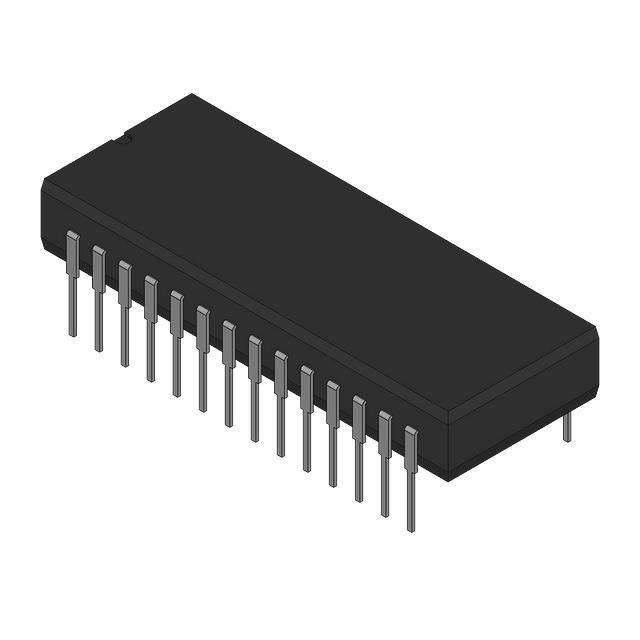
CS61574A CS61575
T1/E1 Line Interface
Features General Description
The CS61574A and CS61575 combine the complete analog transmit and receive line interface for T1 or E1 applications in a low power, 28-pin device operating from a +5V supply. Both devices support processorbased or stand-alone operation and interface with industry standard T1 and E1 framers. The receiver uses a digital Delay-Locked-Loop which is continuously calibrated from a crystal reference to provide excellent stability and jitter tolerance. The CS61574A has a receiver jitter attenuator optimized for minimum delay in switching and transmission applications, while the CS61575 attenuator is optimized for CPE applications subject to AT&T 62411 requirements. The transmitter features internal pulse shaping and a matched, constant impedance output stage to insure signal quality on mismatched, poorly terminated lines.
•
Provides Analog Transmission Line Interface for T1 and E1 Applications
• Provides Line Driver, Jitter Attenuator
and Clock Recovery Functions
• Fully Compliant with AT&T 62411
Stratum 4 Jitter Requirements
• Low Power Consumption
(typically 175 mW)
• B8ZS/HDB3/AMI Encoder/Decoder • 14 dB of Transmitter Return Loss
( ) = Pin Function in Host Mode [ ] = Pin Function in Extended Hardware Mode 2 TCLK TPOS [TDATA] TNEG [TCODE] RCLK RPOS [RDATA] RNEG [BPV] 3 R E M O T E L O O P B A C K 26
Applications
• • •
Interfacing Network Equipment such as DACS and Channel Banks to a DSX-1 Cross Connect Interfacing Customer Premises Equipment to a CSU Building Channel Service Units
ORDERING INFORMATION - See page 26.
(CLKE) (INT) (SDI) (SDO) TAOS LEN0 LEN1 LEN2 28 23 24 25
MODE 5 L O C A L L O O P B A C K
TGND
TV+
15 14 LINE DRIVER 13 16
CONTROL
PULSE SHAPER LINE RECEIVER
TTIP TRING
4
8 7
AMI, B8ZS, HDB3, CODER
19 20 17
JITTER ATTENUATOR
CLOCK & DATA RECOVERY SIGNAL QUALITY MONITOR
RTIP
RRING MTIP [RCODE] MRING [PCS] DPM [AIS]
6
DRIVER MONITOR 22 RGND
18
11 9 10 1 27 LLOOP (SCLK) 12 LOS 21 RV+
RLOOP XTALIN XTALOUT ACLKI (CS)
Crystal Semiconductor Corporation P. O. Box 17847, Austin, Texas, 78760 (512) 445-7222 FAX:(512) 445-7581
Copyright © Crystal Semiconductor Corporation 1996 (All Rights Reserved)
MAY ’96 DS154F2 1
�CS61574A CS61575
ABSOLUTE MAXIMUM RATINGS
Symbol Min Max Units DC Supply RV+ 6.0 V TV+ (RV+) + 0.3 V Input Voltage, Any Pin (Note 1) Vin RGND-0.3 (RV+) + 0.3 V Input Current, Any Pin (Note 2) Iin -10 10 mA Ambient Operating Temperature TA -40 85 °C Storage Temperature Tstg -65 150 °C WARNING:Operations at or beyond these limits may result in permanent damage to the device. Normal operation is not guaranteed at these extremes. Notes: 1. Excluding RTIP, RRING, which must stay within -6V to (RV+) + 0.3V. 2. Transient currents of up to 100 mA will not cause SCR latch-up. Also TTIP, TRING, TV+ and TGND can withstand a continuous current of 100 mA. Parameter (referenced to RGND, TGND=0V)
RECOMMENDED OPERATING CONDITIONS
Symbol Min Typ Max DC Supply (Note 3) RV+, TV+ 4.75 5.0 5.25 Ambient Operating Temperature TA -40 25 85 290 350 Power Consumption (Notes 4,5) PC Power Consumption (Notes 4,6) PC 175 Notes: 3. TV+ must not exceed RV+ by more than 0.3V. 4. Power consumption while driving line load over operating temperature range. Includes IC and Digital input levels are within 10% of the supply rails and digital outputs are driving a 50 pF capacitive load. 5. Assumes 100% ones density and maximum line length at 5.25V. 6. Assumes 50% ones density and 300ft. line length at 5.0V. Parameter Units V °C mW mW load.
DIGITAL CHARACTERISTICS
Parameter
(TA = -40°C to 85°C; TV+, RV+ = 5.0V ±5%; GND = 0V) Symbol Min Typ Max Units V V V V µA V V V
2.0 High-Level Input Voltage (Notes 7, 8) VIH PINS 1-4, 17, 18, 23-28 Low-Level Input Voltage (Notes 7, 8) VIL 0.8 PINS 1-4, 17, 18, 23-28 High-Level Output Voltage (Notes 7, 8, 9) VOH 4.0 IOUT = -40 µA PINS 6-8, 11, 12, 25 0.4 Low-Level Output Voltage (Notes 7, 8, 9) VOL IOUT = 1.6 mA PINS 6-8, 11, 12, 23, 25 Input Leakage Current (Except Pin 5) ±10 Low-Level Input Voltage, PIN 5 VIL 0.2 High-Level Input Voltage, PIN 5 VIH (RV+) - 0.2 Mid-Level Input Voltage, PIN 5 (Note 10) VIM 2.3 2.7 Notes: 7. In Extended Hardware Mode, pins 17 and 18 are digital inputs. In Host Mode, pin 23 is an open drain output and pin 25 is a tristate output. 8. This specification guarantees TTL compatibility (VOH = 2.4V @ IOUT = -40µA). 9. Output drivers will drive CMOS logic levels into a CMOS load. 10. As an alternative to supplying a 2.3-to-2.7V input, this pin may be left floating. 2
DS154F2
�CS61574A CS61575
ANALOG SPECIFICATIONS
Parameter
(TA = -40°C to 85°C; TV+, RV+ = 5.0V ±5%; GND = 0V) Min Typ Max Units
Transmitter AMI Output Pulse Amplitudes (Note 11) 2.14 2.37 2.6 V E1, 75 Ω (Note 12) 2.7 3.0 3.3 V E1, 120 Ω (Note 13) 2.7 3.0 3.3 V T1, FCC Part 68 (Note 14) 2.4 3.0 3.6 V T1, DSX-1 (Note 15) E1 Zero (space) level (LEN2/1/0 = 0/0/0) -0.237 0.237 V 1:1 transformer and 75Ω load -0.3 0.3 V 1:1.26 transformer and 120Ω load Recommended Output Load at TTIP and TRING 75 Ω Jitter Added During Remote Loopback (Note 16) 10Hz - 8kHz 0.005 0.02 UI 8kHz - 40kHz 0.008 0.025 UI 0.010 0.025 UI 10Hz - 40kHz 0.015 0.05 UI Broad Band Power in 2kHz band about 772kHz (Notes 11, 17) 12.6 15 17.9 dBm Power in 2kHz band about 1.544MHz (Notes 11, 17) -29 -38 dB (referenced to power in 2kHz band at 772kHz) Positive to Negative Pulse Imbalance (Notes 11, 17) T1, DSX-1 0.2 0.5 dB E1 amplitude at center of pulse -5 5 % -5 5 % E1 pulse width at 50% of nominal amplitude Transmitter Return Loss (Notes 11, 17, 18) 51 kHz to 102 kHz 8 dB 102 kHz to 2.048 MHz 14 dB 2.048 MHz to 3.072 MHz 10 dB Transmitter Short Circuit Current (Notes 11, 19) 50 mA RMS Driver Performance Monitor MTIP/MRING Sensitivity: Differential Voltage Required for Detection 0.6 V Notes: 11. Using a 0.47 µF capacitor in series with the primary of a transformer recommended in the Applications section. 12. Pulse amplitude measured at the output of a 1:1 or 1:1.26 transformer across a 75 Ω load for line length setting LEN2/1/0 = 0/0/0. 13. Pulse amplitude measured at the output of a 1:1.26 transformer across a 120 Ω load for line length setting LEN2/1/0 = 0/0/0. 14. Pulse amplitude measured at the output of a 1:1.15 transformer across a 100 Ω load for line length setting LEN2/1/0 = 0/1/0. 15. Pulse amplitude measured at the DSX-1 cross-connect across a 100 Ω load for line length settings LEN2/1/0 = 0/1/1, 1/0/0, 1/0/1, 1/1/0, or 1/1/1 using a 1:1.15 transformer and the length of #22 AWG, ABAM, or equivalent cable specified in Table 3. 16. Input signal to RTIP/RRING is jitter free. Values will reduce slightly if jitter free clock is input to TCLK. 17. Not production tested. Parameters guaranteed by design and characterization. 18. Return loss = 20 log10 ABS((z1 +z0)/(z1-z0)) where z1 = impedance of the transmitter, and z0 = impedance of line load. Measured with a repeating 1010 data pattern with LEN2/1/0 = 0/0/0 and a 1:1 transformer terminated with a 75Ω load, or a 1:1.26 transformer terminated with a 120Ω load. 19. Measured broadband through a 0.5 Ω resistor across the secondary of a 1:1.26 transformer during the transmission of an all ones data pattern for LEN2/1/0 = 0/0/0.
DS154F2 3
�CS61574A CS61575
ANALOG SPECIFICATIONS
Parameter
(TA = -40°C to 85°C; TV+, RV+ = 5.0V ±5%; GND = 0V) Min -13.6 500 Typ 50k Max Units Ω dB mV
Receiver RTIP/RRING Input Impedance Sensitivity Below DSX (0dB = 2.4V)
Data Decision Threshold T1, DSX-1 (Note 20) 60 65 70 % of peak T1, DSX-1 (Note 21) 53 65 77 % of peak T1, FCC Part 68 and E1 (Note 22) 45 50 55 % of peak Allowable Consecutive Zeros before LOS 160 175 190 bits Receiver Input Jitter Tolerance (Note 23) 10kHz - 100kHz 0.4 UI 6.0 UI 2kHz 10Hz and below 300 UI Loss of Signal Threshold (Note 24) 0.25 0.30 0.50 V Notes: 20. For input amplitude of 1.2 Vpk to 4.14 Vpk. 21. For input amplitude of 0.5 Vpk to 1.2 Vpk and from 4.14 Vpk to RV+. 22. For input amplitude of 1.05 Vpk to 3.3 Vpk. 23. Jitter tolerance increases at lower frequencies. See Figure 11. 24. The analog input squelch circuit shall operate when the input signal amplitude above ground on the RTIP and RRING pins falls within the range of 0.25V to 0.50V. Operation of the squelch results in the recovery of zeros. During receive LOS, the RPOS, RNEG or RDATA outputs are forced low.
4
DS154F2
�CS61574A CS61575
ANALOG SPECIFICATIONS
Parameter
(TA = -40°C to 85°C; TV+, RV+ = 5.0V ±5%; GND = 0V) Min Typ Max Units
Jitter Attenuator Jitter Attenuation Curve Corner Frequency (Notes 17, 25) CS61574A 6 Hz CS61575 3 Hz CS61574A T1 Receiver Jitter Transfer (Notes 25, 26) Jitter Freq. [Hz] Amplitude [UIpp] 10 10 3.0 6.0 dB 20 30 dB 100 10 500 10 35 40 dB 40 50 dB 1k 5 40 50 dB 10k, 40k 0.3 CS61575 T1 Receiver Jitter Transfer (Notes 25, 26) Jitter Freq. [Hz] Amplitude [UIpp] 6.0 9.0 dB 10 10 100 10 23 33 dB 500 10 38 43 dB 40 50 dB 1k 5 40 50 dB 10k, 40k 0.3 CS61574A E1 Receiver Jitter Transfer (Notes 26, 27, 28) Jitter Freq. [Hz] Amplitude [UIpp] 10 1.5 3.0 6.0 dB 20 1.5 6.0 12 dB 20 32 dB 100 1.5 30 40 dB 400 1.5 1k 1.5 35 45 dB 35 45 dB 10k, 100k 0.2 CS61575 E1 Receiver Jitter Transfer (Notes 26, 27, 28) Jitter Freq. [Hz] Amplitude [UIpp] 10 1.5 6.0 12 dB 12 18 dB 20 1.5 100 1.5 22 29 dB 30 39 dB 400 1.5 35 45 dB 1k 1.5 10k, 100k 0.2 35 45 dB Attenuator Input Jitter Tolerance (Notes 17, 28) (Before Onset of FIFO Overflow or Underflow Protection) CS61574A 12 23 UI CS61575 138 UI Notes: 25. Attenuation measured at the demodulator output of an HP3785B with input jitter equal to 3/4 of measured jitter tolerance using a measurement bandwidth of 1 Hz (10


 工商网监
湘ICP备2023018690号
工商网监
湘ICP备2023018690号
