Semiconductor Corporation
CS8130 CS8130
Multi-Standard Infrared Transceiver
Features General Description
The CS8130 is an infrared transceiver integrated circuit. The receive channel includes on-chip high gain PIN diode amplifier, IrDA, HPSIR, ASK & TV remote compatible decoder, and data pulse stretcher. The transmit path includes IrDA, HPSIR, ASK & TV remote compatible encoder, and LED driver. The computer data port is standard UART TxD and RxD compatible, and operates from 1200 to 115200 baud. External PIN diode and transmit LED are required. A control mode is provided to allow easy UART programming of different modes. The CS8130 operates from power supplies of +2.7V to +5.5V.
• Adds IR port to standard UART • IrDA, HPSIR, ASK (CW) & TV remote
compatible
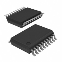
• 1200bps to 115kbps data rate • Programmable Tx LED power • Programmable Rx threshold level • Power down modes • Direct, no modulation, mode • Tiny 5x7mm 20 pin SSOP package • +2.7V to +5.5V supply
Ordering Information: See page 28.
+Supply VA+ 8 PINA
PINC
+Supply VD+ 12
11
RESET RXD RxD
FORM/BSY CTS
6
7
13
P IN Diode Preamplifier
Threshold Detect/Decode
Demodulator
16
+Supply
LED1C 1 LED Driver 1
Modulator
FIFO
Data/Control Decoder
14
TXD
STANDARD UART TxD
LED2C
15
4
D/C
DTR PWRDN
LED Driver 2 3 2 TGND1 5 AGND 19
EXTCLK
Baud Rate Generator
17 18
10
9
20
CLKFR DGND
TGND2
XTALIN XTALOUT
Preliminary Product Information
Crystal Semiconductor Corporation http://www.cirrus.com P.O. Box 17847, Austin, TX 78760 (512) 445-7222 FAX: (512) 445-7581
This document contains information for a new product. Crystal Semiconductor reserves the right to modify this product without notice.
Copyright © Crystal Copyright © Cirrus Logic, Inc. 2005 Semiconductor Corporation 1994 (All Rights Reserved) (All Rights Reserved)
JUN ’94 SEP ‘05 DS134PP2 DS134F1 1
�CS8130
CS8130
TRANSMITTER DRIVER CHARACTERISTICS (TA = 25 °C; All V+ = 3.0V, Digital Input Levels: Logic 0 = 0V, Logic 1 = V+; unless otherwise specified) Parameter Symbol Min 5%)). Typ 10 20 20 Max TBD 50 50 25 0.5 20 250 200 Units pF ns ns % Ω µA mA ns Output capacitance (Note 1) Output rise time (10% to 90%) tr Output fall time (90% to 10%) tf Overshoot over final current On resistance Off leakage current Output current (each driver) (Note 2) Output jitter relative a jitter free input clock Notes: 1. Typical LED junction capacitance is 20pF. 2. 50% duty cycle, max pulse width 165 µs (3/16 of (1/1200 bps +
RECEIVER CHARACTERISTICS (TA = 25 °C; All V+ = 3.0V, Digital Input Levels: Logic 0 = 0V, Logic 1 = V+; unless otherwise specified) Parameter Symbol Min Typ Max Units Input capacitance (Note 3) 10 TBD pF Input noise current 11 pA/rtHz Maximum signal input current from detector 2 mA Maximum DC input current (typically sunlight) 200 µA Input current detection thresholds RS4-0=00000: 7.8 nA (Programmable with a 5 bit value) RS4-0=00001: 15.6 nA 16.4 23.4 30.4 nA (Min, Max = Typical ±30%) RS4-0=00010: " ↓ ↓ ↓ (Note 4) ↓ nA 169.5 242.2 314.9 RS4-0=11110: nA 175 250 325 RS4-0=11111: Bandpass filter response High Pass -3dB: 35 kHz Low Pass -3dB: 700 kHz 5 10 ms Receiver power up time With high (200µA) dc ambient 0.3 1 ms With normal (2µA) dc ambient Turn-around time, with receiver on continuously (Note 5) 5 10 ms EMI rejection of system (0.5MHz to 100MHz). (Note 6) 3 V/m Notes: 3. Typical PIN diode junction capacitance is 50pF. 4. The ±30% tolerance covers chip-to-chip variation. The temperature coefficient of the receiver threshold setting is low. Current detection thresholds are above the DC ambient condition. Settings of RS4-0 of less than 00010 are not practical because of noise. 5. Turn-around time is the time taken for the PIN diode receiver to recover from the IR energy from the transmitter. The remote end of the link must wait for this time after receiving data before transmitting a reply. This time may be reduced to 1 µs). Power Down When the PWRDN pin is brought low, all internal logic is stopped, including the crystal oscillator. The power consumption in power down mode is very low (25 ms if using the crystal oscillator (see Clock Generation above). Control Register Definitions The various control registers within the CS8130 may be written by setting the D/C pin to low, and sending characters from the UART to the TXD pin. The characters are interpreted as a 4bit address field and a 4-bit data field, as shown in Figure 7. After the control character is received and written into the control register, it is optionally echoed back out the RXD pin. The baud rate used for this control mode is whatever is currently set in the baud rate register. If the "load baud rate" bit is written to, then the new baud rate takes effect after the character has been echoed back, if echo is enabled. Otherwise, the new baud rate is effective immediately. One of the control registers contains a shadow register set enable bit, which effectively becomes the MSB of the 5-bit register address. Hence there are 31 4-bit registers. The shadow bit must be written to a 1 to allow access to the registers with addresses 16 through 31. The shadow bit
register is always accessible, independent of the state of the shadow bit. The shadow bit must be written to 0 to enable access to registers 0 through 15. The following tables define the detailed function of all the registers inside the CS8130.
Start Bit TXD D/C CD0
Data CD1 CD2 CD3 AD0
Address AD1 AD2 AD3
Stop Bit
Start Bit RXD CD0
Data
Address
Stop Bit AD3
CD1
CD2
CD3
AD0
AD1
AD2
Figure 7. Control Mode Timing 12 DS134F1 DS134PP2
�CS8130
CS8130
Control Data Byte Format
D7
AD3
D6
AD2
D5
AD1
D4
AD0
D3
CD3
D2
CD2
D1
CD1
D0
CD0
BIT
NAME
AD3-0
Register Address (4 bits of transmitted address + MSB, which is the shadow (SHDW) bit state [Control Reg #3]. All registers have 4 data bits).
VALUE 0_0000 0_0001 0_0010 0_0011 0_0100 0_0101 0_0110 0_0111 0_1000 0_1001 0_1010 0_1011 0_1100 0_1101 0_1110 0_1111 1_0000 1_0001 1_0010 1_0011 1_0100 1_0101 1_0110 1_0111 1_1000 1_1001 1_1010 1_1011 1_1100 1_1101 1_1110 1_1111
FUNCTION
0 1 2 3 4 5 6 7 8 9 10 11 12 13 14 15 16 17 18 19 20 21 22 23 24 25 26 27 28 29 30 31
Control register #1 Control register #2 Transmit Mode Register #1 Transmit Mode Register #2 Output Power register Receive Mode register Receive Sensitivity register #1 Receive Sensitivity register #2 Baud Rate Divider register #1 Baud Rate Divider register #2 Modulator Divider register #1 Modulator Divider register #2 Digital Output Pin Control register Control Register #3 Reserved Status register (read only) TV Remote Receive Sample Rate & T Period Divider TV Remote Receive Sample Rate & T Period Divider TV Remote Receive Sample Rate & T Period Divider TV Remote Transmit Bit Rate Divider #1 TV Remote Transmit Bit Rate Divider #2 Control Register #4 Reserved Reserved ASK Receive Timing Sensitivity register Reserved Reserved Reserved CS8130 Revision Level register (Read Only) Reserved Reserved (Resets to 1111; must not be changed) Reserved (Resets to 1111; must not be changed) Contains control register data.
CD3-0
Control Data
It is essential that all reserved registers and bits are not changed from their reset state. If reserved bits are changed, then internal test modes may be invoked, which may change some input pins to output pins, and may completely change the definition of some functions and signals. Reserved bits in registers, and reserved registers, may not return a known state when read, and should be ignored. Registers 28 and 15 are read only. Other non-reserved registers are write only. The CS8130 can be set to echo back register write commands to verify correct reception of the control settings.
DS134F1 DS134PP2
13 13
�CS8130
CS8130
Register 0, Control Register #1
D3 Register Reset (R) BIT ECHO RXEN TXEN
ECHO
D2
0
D1
RXEN
D0
TXEN
0
0
0
0 VALUE 0 1 0 1 0 1 FUNCTION R Do not echo control characters Echo control characters. R Receiver disabled Receiver enabled R Transmitter disbabled Transmitter enabled
NAME Echo Control Characters Receiver Enable Transmitter Enable
Register 1, Control Register #2
D3 Register Reset (R) BIT AUTD LODB
0
D2
0
D1
AUTD
D0
LODB
0
0
0
0 VALUE 0 1 0 1 FUNCTION R Auto detect receive format disabled Auto detect receive format enabled R Do not load new baud rate count value Load new baud rate count value
NAME Receiver auto detect mode enable Load Baud Rate Counter
The LODB bit resets to 0 automatically.
14
DS134F1 DS134PP2
�CS8130
CS8130
Register 2, Transmit Mode Register #1
D3 Register Reset (R) BIT DIR TVR PWID MODU
DIR
D2
TVR
D1
PWID
D0
MODU
0
0
0
0 VALUE 0 1 0 1 0 1 0 1 R R R R FUNCTION Mode 4 Direct access mode disabled Mode 4 Direct access mode enabled Mode 3 TV remote mode disabled Mode 3 TV remote mode enabled Set pulse width to 1.6 µS Set pulse width to 3/16 of the bit period Mode 1 IrDA pulse modulation enabled Mode 2 Amplitude modulated carrier modulation
NAME Direct Mode Enable TV Remote Mode Enable Select Pulse Width Select Modulation Method
Register 3, Transmit Mode Register #2
D3 Register Reset (R) BIT CHSY BC1-0
0
D2
CHSY
D1
BC1
D0
BC0
0
1
1
0 VALUE 0 1 00 01 10 11 FUNCTION Bits are transmitted based on TXD bit transitions R Bits are transmitted timed from the start bit 6 data bits per character 7 data bits per character R 8 data bits per character 9 data bits ( 8 data, 1 parity) per character
NAME Character/bit synchronized Number of bits per character (only needed if CHSY = 1)
0 1 2 3
Register 4, Output Power Register
D3 Register Reset (R) BIT OP1-0
0
D2
0
D1
OP1
D0
OP0
0
0
0
0 VALUE 00 01 10 11 0 1 2 3 FUNCTION R No LED output enabled LED1C output only enabled LED2C output only enabled Both LED1C and LED2C outputs enabled
NAME Output Power Level
DS134F1 DS134PP2
15 15
�CS8130
CS8130
Register 5, Receive Mode Register
D3 Register Reset (R) BIT RTVR, RMOD, RWIDS, RWIDL 0 D2 0 D1 1 D0 1 VALUE 0000 0001 0010 0011 0100 1000 1100 FUNCTION 0 Mode 2 Amplitude modulated carrier mode 1 Mode 1a IRDA - fixed 1.6µs pulse 2 Mode 1b IRDA - variable 3/16 bit cell time pulse 3 R Mode 1c IRDA - Any width pulse from 1.6µs to 3/16 bit cell time 4 Mode 4 Direct access mode 8 Mode 3 TV remote mode, oversampling receive 12 Mode 3 TV remote mode, timed bit cell receive All other combinations are reserved
RTVR RMOD RWIDS RWIDL
NAME Receive Mode
Register 6, Receive Sensitivity Register #1
D3 Register Reset (R)
RS3
D2
RS2
D1
RS1
D0
RS0
0
1
1
1
Register 7, Receive Sensitivity Register #2
D3 Register Reset (R) BIT RS4-0
0
D2
0
D1
0
D0
RS4
0
0
0
0 VALUE 00000 00001 " 00111 " 11110 11111 FUNCTION 0 7.8 nA nominal receive threshold 1 15.6 nA nominal receive threshold " " 7 R 62.5 nA nominal receive threshold " " 30 242.2 nA nominal receive threshold 31 250 nA nominal receive threshold
NAME Receive threshold setting.
Threshold settings of less than 20nA should not be used because background noise will cause the apparent occurrence of constant signal.
16
DS134F1 DS134PP2
�CS8130
CS8130
Register 8, Baud Rate Divider Register #1
D3 Register Reset (R)
BR3
D2
BR2
D1
BR1
D0
BR0
0
1
1
1
Register 9, Baud Rate Divider Register #2
D3 Register Reset (R) BIT BR7-0
BR7
D2
BR6
D1
BR5
D0
BR4
0
0
0
1 VALUE 01011111 00101111 00010111 00001011 00001001 00000010 00000001 FUNCTION 95 2400 bps 47 4800 bps 23 R 9600 bps 11 19.2 kbps 5 38.4 kbps 2 76.8 kbps 1 115.2 kbps
NAME Baud Rate Divider Value (BRD). BRD=(3.6864E6/ (16*BR))-1, where BRD = divider value and BR = desired baud rate.
Register 10, Modulator Divider Register #1
D3 Register Reset (R)
MD3
D2
MD2
D1
MD1
D0
MD0
0
1
1
0
Register 11, Modulator Divider Register #2
D3 Register Reset (R) BIT MD7-0
MD7
D2
MD6
D1
MD5
D0
MD4
0
0
0
0 VALUE 01100000 96 38 kHz 00000110 6 R 527kHz FUNCTION
NAME Modulator Divider Value (MD). MD=(3.6864E6/FR)1, where MD = divider value and FR = desired modulation frequency.
The transmitted modulation frequency will be exact. The receive carrier detection frequency can be slightly different from the programmed frequency (see Receive ASK Carrier Timing Register).
DS134F1 DS134PP2
17 17
�CS8130
CS8130
Register 12, Output Pin Control Register
D3 Register Reset (R) BIT RXDT RXDH FORT 0 D2 1 D1
FORT
D0
FORH
RXDT RXDH
0
1 VALUE 0 1 0 1 0 1 0 1 R In In In R In R In In power power power power power power down, down, down, down, down, down, FUNCTION RXD will go high or low. RXD will float. RXD will go low, if RXDT = 0 RXD will go high, if RXDT = 0 FORM/BSY will go high or low. FORM/BSY will float.
FORH
NAME RXD output pin three-state enable RXD output pin high/low enable FORM/BSY output pin three-state enable FORM/BSY output pin high/low enable
In power down, FORM/BSY will go low, if FORT = 0 R In power down, FORM/BSY will go high, if FORT = 0
Register 13, Control Register #3
D3 Register Reset (R) BIT SHDW
0
D2
0
D1
0
D0
SHDW
0
0
0
0 VALUE 0 1 FUNCTION R Enable access to registers 0 though 15 Enable access to shadow registers (16 through 31)
NAME Shadow register set enable
Register 15, Status Register
D3 Register Reset (R) BIT OSCR
0
D2
OSCR
D1
ERR
D0
DMOD
0
0
0 VALUE 0 1 0 1 0 1 FUNCTION Oscillator not running, using external clock input, oscillator circuit is powered down. Oscillator running, EXTCLK is an output, if enabled. R No error A framing error has occurred since the last read of this bit. Resets after read R IrDA pulse style data format detected Amplitude modulated carrier style data format detected
NAME Oscillator running flag Framing error flag
ERR
DMOD
Detected Modulation Type
To read this register, write 0000 to address 15. Independent of the setting of the ECHO bit, the CS8130 will transmit the above contents, with an address field of 1111.
18 DS134F1 DS134PP2
�CS8130
CS8130
Register 16, TV Remote Receive Timing Register #1
D3 Register Reset (R) 1 D2 1 D1 1 D0
TVR0 TVR3 TVR2 TVR1
1
Register 17, TV Remote Receive Timing Register #2
D3 Register Reset (R)
TVR7
D2
TVR6
D1
TVR5
D0
TVR4
1
1
1
1
Register 18, TV Remote Receive Timing Register #3
D3 Register Reset (R) BIT TVR11-0 0 D2 1 D1
TVR9
D0
TVR8
TVR11 TVR10
1
1 VALUE 000000000000 000000000001 ↓ 011111111111 ↓ 111111111111 FUNCTION 0 1 ↓ 2047R ↓ 4095 T = 271 ns T = 542 ns ↓ T = 555 µs (1800 bps) ↓ T = 1.11 ms
NAME TV remote mode receiver timing register TVR = (3.6864E6 * T) -1 where T = the incoming bit period, and TVR = this register value.
For TV remote receive "oversampled" mode, this register value determines the input data sample rate. The sample rate is 3.6864 MHz divided by this register value. The sample rate should be set to as fast as possible, to give the best resolution on the incoming data edges, but should be less than 80% of the main UART communication baud rate. For TV remote receive "programmed T period" mode, this register sets the expected incoming bit cell time (T). The main UART communications rate must be set to at least 20% greater than 1/T.
DS134F1 DS134PP2
19 19
�CS8130
CS8130
Register 19, TV Remote Transmit Bit Rate Divider Register #1
D3 Register Reset (R) 1 D2 1 D1 1 D0
TBR0 TBR3 TBR2 TBR1
1
Register 20, TV Remote Transmit Bit Rate Divider Register #2
D3 Register Reset (R) BIT TBR7-0
TBR7
D2
TBR6
D1
TBR5
D0
TBR4
0
1
1
1 VALUE 01111111 127 R FUNCTION RATE = 1800 bps
NAME TV remote mode transmit bit rate register TBR= (3.6864E6/(16*RATE)) -1 where TBR is this register value & RATE is the desired transmit bit rate.
Register 21, Control Register #4
D3 Register Reset (R) BIT OSCE 0 D2 0 D1 0 D0
SRES OSCE OSCL EXCK
0 VALUE 0 1 0 1 0 1 0 1 FUNCTION R In D/C controlled power down state, crystal oscillator stays running. In D/C controlled power down state, crystal oscillator stops. R Oscillator in normal power, high accuracy, mode. Oscillator in low power, medium accuracy mode. R If crystal is used, enable clock output driver If crystal is used, disable clock output driver (Hi-Z) R Normal operation Causes a software reset, which forces all registers into their reset state. If ECHO is true, then the echo will occur at the current baud rate, before the baud rate changes to the default value.
OSCL EXCK SRES
NAME Disable crystal oscillator in D/C controlled power down state Set oscillator in low power mode Disable external clock output driver Software Reset
20
DS134F1 DS134PP2
�CS8130
CS8130
Register 24, Receive ASK Timing Sensitivity Register
D3 Register Reset (R) BIT RAT3-0 0 D2 0 D1 0 D0
RAT0 RAT3 RAT2 RAT1
0 VALUE 0000 0001 0010 ↓ 1111 0 R +0.27 1 +0.27 2 +0.27 ↓ 15 +0.27 FUNCTION µs to -0.27 µs window (500 kHz ASK mode) µs to -0.54 - 0.27 µs window µs to -1.08 - 0.27 µs window ↓ µs to -8.14 - 0.27 µs window
NAME Receiver ASK Timing Sensitivity. Timing window = +0.27 µs to -RAT(2/3.6864E06) - 0.27 µs
The timing window is relative to the modulation divider register nominal setting.
Register 28, CS8130 Silicon Revision Register
D3 Register D2 D1 D0
REV0 REV3 REV2 REV1
BIT REV3-0
NAME CS8130 silicon revision level
VALUE 0000
FUNCTION 1st silicon, designed to meet DS134PP2 data sheet, dated June 1994
This register should be read by the CS8130 driver to allow CS8130 future enhancements to be recognized, and incorporated into future versions of the driver.
DS134F1 DS134PP2
21 21
�CS8130
CS8130
Grounding & Layout Grounding and layout for the CS8130 are critical, because of the sensitive nature of the PIN diode amplifier. The CS8130 should be over its own dedicated ground plane. The PIN diode should be very close to the PINA and PINC pins. The PIN diode traces should be very short (< 5 mm), and should be surrounded by ground plane. There should be holes in the ground plane provided for mounting a metal shield over the CS8130 and the PIN diode for EMI shielding. The PIN diode and transmit LEDs should be positioned so as to line up the front optical surfaces of the packages. The optical surface of the PIN diode and transmit LED(s) should be positioned 1cm back from the daylight IR filter window inside the case of the equipment. This ensures that direct sunlight does not fall upon the top surface of the PIN diode. An evaluation kit, CDB8130, is available from Crystal. This may be used as an example of the correct layout for the CS8130 and the optical components.
Optical Components TEMIC (Tel: 408 970 5684) provides Telefunken infrared LEDs and PIN diodes which are compatible with the CS8130. Contact Crystal for details of additional qualified LED and PIN diode sources. Example Application Schematics Crystal has prepared some example schematics which demonstrate possible uses for the CS8130. Figure 8 shows a computer or PDA motherboard example, where one UART is used to drive both a wired RS232 COM port and an IR port. Figure 9 shows a pod schematic. This is an external unit which can be plugged into any existing COM port to create an IR port.
Schematic & Layout Review Service
Confirm Optimum Schematic & Layout Before Building Your Board. For Our Free Review Service Call Applications Engineering.
Call: (512) 445-7222
22
DS134F1 DS134PP2
�CS8130
CS8130
10 Ω 10 µF + 0.1 µF 8 VA+ 5 7
BPV23NF
0.1 µF 12 VD+ 19 EXTCLK XTALIN XTALOUT 17
+
+3V 10 µF Notes: (1) This circuit has not yet been built and debugged. (2) Choice of LED, power consumption and physical positioning will affect R value. 3.6864 MHz
AGND PINC PINA
18 11 13 16 14 15 10 9
6 TSHA5502 + +3V 47 µF 5.2 Ω (2) 5.2 Ω (2) 1 4
RESET
CS8130
LED1C LED2C
RXD
FORM/BSY TXD D/C PWRDN CLKFR TGND1 TGND2 DGND 2 3 20
+3V 0.33 µF 1 5 0.33 µF VCC CIAEN SHDN
C2+
14 15 25 24 0.33 µF
2 CIA+ 4
CIB-
RS-232/IR SELECT
0.33 µF
3
MAX562
CIB+ C2-
UART
DSR CTS RXD DCD RI DTR RTS TXD
6 8 2 DB9 1 Serial Connector 9 (COM PORT) 4 7 3 5
DSR CTS RXD DCD
RI
23 R1IN 22 R2IN 21 R3IN 20 R4IN
19 R5IN
R1OUT 6 R2OUT 7 R3OUT 8 R4OUT 9
R5OUT 10
DTR
RTS
18 T1OUT
17 T2OUT
T1IN 11
T2IN 12
TXD SG
16 T3OUT
T3IN 13
V-
26
V+ 28
GND 27
0.68 µF
0.33 µF
UART to both RS232 and IR Port Interface Motherboard Example Schematic
Steven Harris Crystal Semiconductor 5/26/94
Figure 8. IR and RS232 from 1 UART
DS134F1 DS134PP2
23 23
�CS8130
CS8130
10 Ω 10 µF + 0.1 µF 8 VA+ 5 7
BPV23NF
0.1 µF 12 VD+ EXTCLK XTALIN 19 17
+
+3V 10 µF 1 5 0.33 µF VCC CIACIB0.33 µF
+3V
4 0.33 µF
AGND PINC
2 CIA+
CIB+ 3 C2+ C225 24
CS8130
6 PINA XTALOUT RXD 18 13
3.6864 MHz 11
0.33 µF
RXD CTS TXD
TSHA5502 + +3V 47 µF 5.5 Ω (2) 5.5 Ω (2) 1 4
LED1C LED2C
16 FORM/BSY 14 TXD 15 D/C 11 RESET PWRDN CLKFR 10 9 +3V +3V
T1IN 12 T2IN 6 R1OUT 7 R2OUT 8 R3OUT 14 EN
MAX562
T1OUT 18 T2OUT 17 23 R1IN 22 R2IN 21 R3IN V26
2 8 3 4 7 5
DTR RTS
15 SHDN GND 27
V+ 28 0.68 µF
TGND1 TGND2 DGND 2 3 20
DB9 Serial Connector (COM PORT) 0.33 µF
Notes: (1) This circuit has not yet been built and debugged. (2) Choice of LED, power consumption and physical positioning will affect R value. (3) The creation of +3V or +5V supply is not included here.
RS232 COM PORT to Infra Red Interface Pod Schematic Steven Harris Crystal Semiconductor 5/26/94
Figure 9. Example Pod Schematic
24
DS134F1 DS134PP2
�CS8130
CS8130
LED1 CATHODE TRANSMIT GROUND 1 TRANSMIT GROUND 2 LED2 CATHODE ANALOG GROUND PIN DIODE ANODE PIN DIODE CATHODE ANALOG SUPPLY CLOCK FREQUENCY POWER DOWN
LED1C TGND1 TGND2 LED2C AGND PINA PINC VA+ CLKFR PWRDN
1 2 3 4 5 6 7 8 9 10
20 19 18 17 16 15 14 13 12 11
DGND EXTCLK XTALOUT XTALIN FORM/BSY D/C TXD RXD VD+ RESET
DIGITAL GROUND EXTERNAL CLOCK CRYSTAL OUTPUT CRYSTAL INPUT FORMAT/BUSY DATA/CONTROL TRANSMIT DATA RECEIVE DATA DIGITAL SUPPLY RESET
Power Supplies VD+ - Digital Positive Supply. Digital positive supply voltage. Nominally +3V VA+ - Analog Positive Supply. Analog positive supply voltage. Nominally +3V. DGND - Digital Ground. Digital ground, 0V, connection. AGND - Analog Ground. Analog ground, 0V, connection. TGND1, TGND2 - Transmitter Grounds. LED Transmitter grounds, 0V, connections. Analog Pins LED1C, LED2C - Transmit LED Cathode. These pins are connected to the transmit LED cathode via resistors. Appropriate resistor choice allows user setting of LED current options. The anode of the LED is connected to the positive supply. PINC - Receiver PIN Diode Cathode Receiver PIN diode cathode. PINA - Receiver PIN Diode Anode. Receiver PIN diode anode.
DS134F1 DS134PP2
25 25
�CS8130
CS8130
Digital Pins RXD - Receiver Data Output Receiver output data. Normally connected to RxD on the UART. TXD - Transmit Data Input Transmitter input data. Normally connected to TxD on the UART. D/C - Data/Control Mode Input The D/C pin determines whether the input data on TXD is treated as data to be transmitted via the LED, or as control information to set up the CS8130 internal registers. The D/C pin also can act as a power down control. FORM/BSY - Received Data Format Output/Busy Signal Output If auto format detect mode is enabled, this pin indicates the format of the incoming data. FORM is low for ASK format data, and high for IRDA/HPSIR format data. In TV remote data mode (Mode 3), this pin becomes a handshake signal to the UART. FORM/BSY low means OK to send a character. FORM/BSY high means "I am busy, do not send another character". PWRDN - Power Down Control Input PWRDN low places the CS8130 into a very low power consumption "off" state. RESET - Reset Input RESET low places all the internal logic into a known state. All the control register bits are forced high or low, as defined in the register definition section. If the crystal oscillator is in use, then RESET must be held low for >25 ms, with PWRDN high and power applied. If an external clock is used, then the RESET pulse can be short (>1 µs). XTALIN, XTALOUT - Crystal Connections To use the internal oscillator, connect either a 3.6864 MHz or a 1.8432 MHz crystal between XTALOUT and XTALIN. If using an external clock, connect XTALIN to DGND. EXTCLK - External Clock Input or Output If no crystal is present on XTALIN and XTALOUT, EXTCLK becomes an input. A 3.6864 MHz or 1.8432 MHz clock should be connected to EXTCLK. XTALIN should be connected to DGND. If a crystal is present on XTALIN and XTALOUT, EXTCLK becomes an output. EXTCLK will output the same frequency as the crystal. The EXTCLK output driver may be disabled to conserve power. CLKFR - Clock Frequency Select Input Tie CLKFR to ground to select a 3.6864 MHz clock. Connect CLKFR to the VD+ pin to select a 1.8432 MHz clock.
26
DS134F1 DS134PP2
�CS8130
20 PIN SSOP 28 PIN SSOP
N
E
SSOP Package Dimensions
123
TOP VIEW
D1 A2 A1 b2 Seating Plane
A
E 11
e
L
END VIEW
SIDE VIEW
MILLIMETERS DIM MIN 0.05 1.62 0.22 7.40 5.00 0.61 0.63 0° NOM 0.15 1.75 0.30 7.80 5.30 0.65 0.90 4° MAX 2.13 0.25 1.88 0.38 8.20 5.60 0.69 1.03 8° MIN 0.002 0.009 INCHES NOM MAX Note 0.084
Notes: 1. "D" and "E 1 " are reference datums and do not include mold flash or protrusions, but do include mold mismatch and are measured at the parting line, mold flash or protrusions shall not exceed 0.20mm per side. 2. Dimension b does not include dambar protrusion/intrusion. Allowable dambar protrusion shall be 0.13mm total in excess of b dimension at maximum material condition. Dambar intrusion shall not reduce dimension b by more than 0.07mm at least material condition. 3. These dimensions apply to the flat section of the lead between 0.10 and 0.25mm from lead tips.
A A1 A2 b D E E1 e L N
0.006 0.010 0.012 0.015 2, 3 1 1
0.064 0.070 0.074 see other table 0.291 0.307 0.323 0.197 0.209 0.220 0.024 0.026 0.027 0.025 0° D 0.035 0.040 4° 8° see other table
see other table
∝
N 20 28
see other table
MILLIMETERS MIN 6.90 9.90 NOM 7.20 MAX 7.50 MIN
INCHES NOM MAX 0.413 Note 1 1 0.272 0.283 0.295
10.20 10.50 0.390 0.402
44 DS134F1
27
�CS8130
ORDERING INFORMATION
Model Package Temperature
CS8130-CS
20-pin SSOIC
0 to +70 °C
ENVIRONMENTAL, MANUFACTURING, & HANDLING INFORMATION
Model Number Peak Reflow Temp 240 °C MSL Rating* 2 Max Floor Life 365 Days
CS8130-CS
* MSL (Moisture Sensitivity Level) as specified by IPC/JEDEC J-STD-020.
REVISION HISTORY
Revision PP2 F1 Date JUN 1994 SEP 2005 Initial Release Updated device ordering info. Updated legal notice. Added MSL data.. Changes
Contacting Cirrus Logic Support
For all product questions and inquiries contact a Cirrus Logic Sales Representative. To find the one nearest to you go to www.cirrus.com
IMPORTANT NOTICE Cirrus Logic, Inc. and its subsidiaries (“Cirrus”) believe that the information contained in this document is accurate and reliable. However, the information is subject to change without notice and is provided “AS IS” without warranty of any kind (express or implied). Customers are advised to obtain the latest version of relevant information to verify, before placing orders, that information being relied on is current and complete. All products are sold subject to the terms and conditions of sale supplied at the time of order acknowledgment, including those pertaining to warranty, indemnification, and limitation of liability. No responsibility is assumed by Cirrus for the use of this information, including use of this information as the basis for manufacture or sale of any items, or for infringement of patents or other rights of third parties. This document is the property of Cirrus and by furnishing this information, Cirrus grants no license, express or implied under any patents, mask work rights, copyrights, trademarks, trade secrets or other intellectual property rights. Cirrus owns the copyrights associated with the information contained herein and gives consent for copies to be made of the information only for use within your organization with respect to Cirrus integrated circuits or other products of Cirrus. This consent does not extend to other copying such as copying for general distribution, advertising or promotional purposes, or for creating any work for resale. CERTAIN APPLICATIONS USING SEMICONDUCTOR PRODUCTS MAY INVOLVE POTENTIAL RISKS OF DEATH, PERSONAL INJURY, OR SEVERE PROPERTY OR ENVIRONMENTAL DAMAGE (“CRITICAL APPLICATIONS”). CIRRUS PRODUCTS ARE NOT DESIGNED, AUTHORIZED OR WARRANTED FOR USE IN AIRCRAFT SYSTEMS, MILITARY APPLICATIONS, PRODUCTS SURGICALLY IMPLANTED INTO THE BODY, AUTOMOTIVE SAFETY OR SECURITY DEVICES, LIFE SUPPORT PRODUCTS OR OTHER CRITICAL APPLICATIONS. INCLUSION OF CIRRUS PRODUCTS IN SUCH APPLICATIONS IS UNDERSTOOD TO BE FULLY AT THE CUSTOMER'S RISK AND CIRRUS DISCLAIMS AND MAKES NO WARRANTY, EXPRESS, STATUTORY OR IMPLIED, INCLUDING THE IMPLIED WARRANTIES OF MERCHANTABILITY AND FITNESS FOR PARTICULAR PURPOSE, WITH REGARD TO ANY CIRRUS PRODUCT THAT IS USED IN SUCH A MANNER. IF THE CUSTOMER OR CUSTOMER'S CUSTOMER USES OR PERMITS THE USE OF CIRRUS PRODUCTS IN CRITICAL APPLICATIONS, CUSTOMER AGREES, BY SUCH USE, TO FULLY INDEMNIFY CIRRUS, ITS OFFICERS, DIRECTORS, EMPLOYEES, DISTRIBUTORS AND OTHER AGENTS FROM ANY AND ALL LIABILITY, INCLUDING ATTORNEYS' FEES AND COSTS, THAT MAY RESULT FROM OR ARISE IN CONNECTION WITH THESE USES. Cirrus Logic, Cirrus, and the Cirrus Logic logo designs are trademarks of Cirrus Logic, Inc. All other brand and product names in this document may be trademarks or service marks of their respective owners.
Smart AnalogTM is a Trademark of Crystal Semiconductor Corporation
28 DS134F1
�


 工商网监
湘ICP备2023018690号
工商网监
湘ICP备2023018690号
