CPC1909
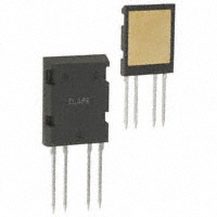
ISOPLUS™-264 Power Relay
Description
Clare and IXYS have combined to bring OptoMOS® technology, reliability, and compact size to a new family of high-power Solid State Relays. As part of this family, the CPC1909 single pole normally open (1-Form-A) Solid State Power Relay is rated for up to 15Arms continuous load current with a 5ºC/W heat sink. The CPC1909 employs optically coupled MOSFET technology to provide 2500Vrms of input to output isolation. The output is constructed with efficient MOSFET switches and photovoltaic die that use Clare’s patented OptoMOS architecture while the input, a highly efficient GaAlAs infrared LED provides the optically coupled control. The combination of low on-resistance and high load current handling capability makes this relay suitable for a variety of high performance switching applications. The unique ISOPLUS-264 package pioneered by IXYS allows Solid State Relays to achieve the highest load current and power ratings. This package features a unique IXYS process where the silicon chips are soft soldered onto the Direct Copper Bond (DCB) substrate instead of the traditional copper leadframe. The DCB ceramic, the same substrate used in high power modules, not only provides 2500Vrms isolation but also very low thermal resistance (0.3 °C/W).
Parameter Blocking Voltage Load Current, TA=25ºC With 5°C/W Heat Sink No Heat Sink On-resistance RθJC
Rating 60 15 6.5 0.1 0.3
Units VP
Arms Ω ºC/W
Features
• • • • • • • • • Compact ISOPLUS-264 Power Package Low Thermal Resistance (0.3 °C/W) 15Arms Load Current with 5°C/W Heat Sink Electrically Non-conductive Thermal Pad for Heat Sink Applications Low Drive Power Requirements Arc-Free With No Snubbing Circuits 2500Vrms Input/Output Isolation No EMI/RFI Generation Machine Insertable, Wave Solderable
Applications
• • • • • Industrial Controls Motor Control Robotics Medical Equipment—Patient/Equipment Isolation Instrumentation • Multiplexers • Data Acquisition • Electronic Switching • I/O Subsystems • Meters (Watt-Hour, Water, Gas) • Transportation Equipment • Aerospace/Defense
Approvals
• UL recognized component: File # E69938 • Certified to: UL 508
Ordering Information
Part Number CPC1909J Description ISOPLUS-264 (25 per tube)
Pin Configuration
Switching Characteristics of Normally Open (Form A) Devices
CONTROL
ILOAD
+ 90% 10%+
RoHS
2002/95/EC
e3
www.clare.com
TON
TOFF
DS-CPC1909-R03
1
�CPC1909
Absolute Maximum Ratings
Parameter Blocking Voltage Reverse Input Voltage Input Control Current Peak (10ms) Input Power Dissipation Isolation voltage Input to Output Operational Temperature Storage Temperature Ratings 60 5 100 1 150 2500 -40 to +85 -40 to +125 Units VP V mA A mW Vrms °C °C Absolute Maximum Ratings are stress ratings. Stresses in excess of these ratings can cause permanent damage to the device. Functional operation of the device at conditions beyond those indicated in the operational sections of this data sheet is not implied.
Electrical absolute maximum ratings are at 25°C
Electrical Characteristics
Parameter Output Characteristics, Load Current 1 Peak Continuous Continuous Continuous On-Resistance 2 Off-State Leakage Current Switching Speeds Turn-On Turn-Off Output Capacitance Input Characteristics, Input Control Current 3 Input Dropout Current Input Voltage Drop Reverse Input Current Common Characteristics, Capacitance Input to Output
1 2 3
Conditions TA = 25°C t ≤ 10ms No Heat Sink TC=25°C TC=99°C IF=10mA, IL=1A VL=60V
Symbol
Min
Typ
Max
Units
IL IL(99) RON ILEAK TON TOFF COUT IF IF VF IR CI/O -
0.6 0.9 -
0.05 15 0.3 4000 1.2 1
25 6.5 15 7.85 0.1 1 25 10 10 1.4 10 -
AP Arms Ω µA
IF=20mA, VL=10V V=25V, f=1MHz TA = 25°C IL=1A IF=5mA VR=5V TA = 25°C -
ms pF mA mA V µA pF
Proper heat sinking required for maximum continuous load current. Measurement taken within 1 second of on time. For applications requiring high temperature operation (TC > 60°C) an LED drive current of 20mA is recommended.
2
www.clare.com
R03
�CPC1909
Thermal Characteristics
Parameter Thermal Resistance (junction to case) Thermal Resistance (junction to ambient) Junction Temperature (operation) Conditions Free air Symbol RθJC RθJA TJ Min -40 Typ 33 Max 0.3 100 Units °C/W °C/W °C
Thermal Management
Device high current characterization was performed using Kunze heat sink KU 1-159, phase change thermal interface material KU-ALC 5, and transistor clip KU 4-499/1. This combination provided an approximate junction-to-ambient thermal resistance of 12.5°C/W.
Heat Sink Calculation
Higher load currents are possible by using lower thermal resistance heat sink combinations. Heat Sink Rating
RθCA =
(TJ - TA) IL(99)2 IL
2
•
RθJC
- RθJC
TJ = Junction Temperature (°C), TJ ≤ 100°C * TA = Ambient Temperature (°C) IL(99) = Load Current with Case Temperature @ 99°C (Arms) IL = Desired Operating Load Current (Arms), IL ≤ IL(MAX) RθJC = Thermal Resistance, Junction to Case (°C/W) = 0.3°C/W RθCA = Thermal Resistance of Heat Sink & Thermal Interface Material , Case to Ambient (°C/W) * Elevated junction temperature reduces semiconductor lifetime.
R03
www.clare.com
3
�CPC1909
PERFORMANCE DATA*
CPC1909 Typical LED Forward Voltage Drop (N = 50, TA = 25ºC, I L = 1ADC, I F = 10mA) CPC1909 Typical On-resistance Distribution (N = 50, TA = 25ºC, I L = 1ADC, I F = 10mA) CPC1909 Typical Turn-On Time (N = 50, TA = 25ºC, I L = 1ADC, I F = 20mA)
35 30 Device Count (N)
35 30 Device Count (N) 25 20 15 10 5 0
35 30 Device Count (N) 25 20 15 10 5 0
25 20 15 10 5 0 1.30 1.31 1.32 1.33 1.34 LED Forward Voltage (V)
0.033
0.037 0.041 0.045 0.049 On-resistance (Ω)
0.053
10.0
12.5
15.0
17.5
20.0
22.5
Turn-On (ms)
25 20 15 10 5 0
CPC1909 Typical Turn-Off Time (N = 50, TA = 25ºC, I L = 1ADC, I F = 20mA)
Load Current (Arms)
CPC1909 Maximum Load Current vs. Temperature with Heat Sink (IF = 20mA)
20 1ºC/W Leakage (µA) 15
CPC1909 Typical Leakage vs. Temperature at Maximum Rated Voltage (Measured across Pins 1 & 2)
0.014 0.012 0.010 0.008 0.006 0.004 0.002 0 -40 -20 0 20 40 60 80 100
Device Count (N)
10
5ºC/W 10ºC/W
5 No Heat Sink 0
0.17
0.23
0.29
0.35
0.41
0.47
0
20
40
60
80
100
Turn-Off (ms)
Temperature (ºC)
Temperature (ºC)
CPC1909 Normalized Blocking Voltage vs. Temperature
84 Blocking Voltage (VP) 82 Turn-On (ms) 80 78 76 74 72 70 68 -40 -20 0 20 40 60 80 100 Temperature (ºC) 42 36 30 24 18 12 6 0 -40
CPC1909 Typical Turn-On vs. Temperature (IL = 1ADC)
IF = 10mA
Turn-Off (ms)
0.48 0.42 0.36 0.30 0.24 0.18 0.12 0.06
CPC1909 Typical Turn-Off vs. Temperature (IL = 1ADC)
IF = 20mA
IF = 20mA
IF = 10mA
-20
0
20
40
60
80
100
-40
-20
0
Temperature (ºC)
20 40 60 Temperature (ºC)
80
100
CPC1909 Typical LED Forward Voltage Drop vs. Temperature
LED Forward Voltage Drop (V) 1.8 1.6 Turn-On (ms) 1.4 1.2 1.0 0.8 -40 -20 0 20 40 60 80 Temperature (ºC) 100 120
CPC1909 Typical Turn-On vs.LED Forward Current (Load Current = 1ADC)
120 100
0.45 0.40 0.35 Turn-Off (ms) 0.30 0.25 0.20 0.15 0.10 0.05 0.00
CPC1909 Typical Turn-Off vs. LED Forward Current (Load Current = 1ADC)
IF = 50mA IF = 20mA IF = 10mA
80 60 40 20 0 0 5 10 15 20 25 30 35 40 45 50 LED Forward Current (mA)
0
5
10
15
20
25
30
35
40
45
50
LED Forward Current (mA)
Unless otherwise specified, all performance data was acquired without the use of a heat sink. *The Performance data shown in the graphs above is typical of device performance. For guaranteed parameters not indicated in the written specifications, please contact our application department.
4
www.clare.com
R03
�CPC1909
PERFORMANCE DATA*
CPC1909 Typical IF for Switch Operation vs. Temperature (IL = 1ADC)
5.0 4.5 4.0 3.5 3.0 2.5 2.0 1.5 1.0 0.5 0
0.060 0.058
CPC1909 Typical On-resistance vs. Temperature (IL = 1ADC)
IF = 10mA
0.054 0.052 0.050 0.048 0.046
-40
-20
0
20
40
60
80
100
0.044 -40
-20
0
Temperature (ºC)
20 40 60 Temperature (ºC)
80
100
Load Current (A)
0.056
10 8 6 4 2 0 -2 -4 -6 -8 -10 -0.54
CPC1909 Typical Load Current vs. Load Voltage (TA = 25ºC, I F = 10mA)
LED Current (mA)
On-resistance (Ω)
-0.36
-0.18
0
0.18
0.36
0.54
Load Voltage (V)
CPC1909 Typical On-resistance vs. Temperature (Load Current = max rated)
0.09 0.08 On-resistance (Ω) 0.07 0.06 0.05 0.04 0.03 0.02 0.01 0.00 -40 -20 0 20 40 60 Temperature (ºC) 80 100 30
CPC1909 Energy Rating Curve (Free air, no heat sink)
25 Load Current (AP) 20 15 10 5 0 10µs 100µs 1ms 10ms 100ms Time
IF = 10mA
1s
10s 100s
Unless otherwise specified, all performance data was acquired without the use of a heat sink. *The Performance data shown in the graphs above is typical of device performance. For guaranteed parameters not indicated in the written specifications, please contact our application department.
R03
www.clare.com
5
�CPC1909
MANUFACTURING INFORMATION
Soldering For proper assembly, the component must be processed in accordance with the current revision of IPC/JEDEC standard J-STD-020. Failure to follow the recommended guidelines may cause permanent damage to the device resulting in impaired performance and/or a reduced lifetime expectancy. Washing Clare does not recommend ultrasonic cleaning or the use of chlorinated solvents.
RoHS
2002/95/EC
e3
MECHANICAL DIMENSIONS:
4-Pin ISOPLUS-264
0.190 MIN - 0.205 MAX (4.83 MIN - 5.21 MAX) 0.046 MIN - 0.055 MAX (1.17 MIN - 1.40 MAX) 0.770 MIN - 0.799 MAX (19.56 MIN - 20.29 MAX) 0.210 MIN - 0.235 MAX (5.33 MIN - 5.97 MAX) 0.100 MIN - 0.180 MAX (2.54 MIN - 4.57 MAX) 0.065 MIN - 0.080 MAX (1.65 MIN - 2.03 MAX) 0.668 MIN - 0.690 MAX (16.97 MIN - 17.53 MAX)
1.020 MIN - 1.040 MAX (25.91 MIN - 26.42 MAX)
0.490 MIN - 0.513 MAX (12.54 MIN - 13.03 MAX)
0.801 MIN - 0.821 MAX (20.34 MIN - 20.85 MAX)
0.100 MIN - 0.130 MAX (2.54 MIN - 3.03 MAX) 1 2 3 4
0.080 MIN - 0.102 MAX (2.03 MIN - 2.59 MAX) 0.780 MIN - 0.820 MAX (19.81 MIN - 20.83 MAX)
0.300 BSC (7.62) BSC
0.150 BSC (3.81 BSC)
0.020 MIN - 0.029 MAX (0.51 MIN - 0.74 MAX)
0.058 MIN - 0.068 MAX (1.47 MIN - 1.73 MAX) 0.102 MIN - 0.118 MAX (2.59 MIN - 3.00 MAX) 0.045 MIN - 0.055 MAX (1.14 MIN - 1.40 MAX)
DIMENSIONS: INCHES (MM) NOTE: Bottom heatsink meets 2500Vrms isolation to the pins.
Dimensions: inches (mm) For additional information please visit our website at: www.clare.com
Clare, Inc. makes no representations or warranties with respect to the accuracy or completeness of the contents of this publication and reserves the right to make changes to specifications and product descriptions at any time without notice. Neither circuit patent licenses nor indemnity are expressed or implied. Except as set forth in Clare’s Standard Terms and Conditions of Sale, Clare, Inc. assumes no liability whatsoever, and disclaims any express or implied warranty, relating to its products including, but not limited to, the implied warranty of merchantability, fitness for a particular purpose, or infringement of any intellectual property right. The products described in this document are not designed, intended, authorized or warranted for use as components in systems intended for surgical implant into the body, or in other applications intended to support or sustain life, or where malfunction of Clare’s product may result in direct physical harm, injury, or death to a person or severe property or environmental damage. Clare, Inc. reserves the right to discontinue or make changes to its products at any time without notice.
DS-CPC1909-R03 ©Copyright 2007, Clare, Inc. OptoMOS® is a registered trademark of Clare, Inc. ISOPLUS™ is a trademark of IXYS Corporation All rights reserved. Printed in USA. 3/20/07
�


 工商网监
湘ICP备2023018690号
工商网监
湘ICP备2023018690号
