CPC5603
N Channel Depletion Mode FET
Parameter Drain-to-Source Voltage (VDS) Max On-Resistance (Ron-max) Max Power
Rating 415 14 2.5
Units V Ω W
Description
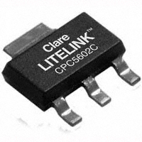
The CPC5603 is an “N” channel depletion mode Field Effect Transistor (FET) that utilizes Clare’s proprietary third generation vertical DMOS process. The third generation process realizes world class, high voltage MOSFET performance in an economical silicon gate process. The vertical DMOS process yields a highly reliable device particularly in difficult application environments such as telecommunications. One of the primary applications for the CPC5603 is as a linear regulator/ hook switch for the LITELINK™ family of Data Access Arrangements (DAA) Devices CPC5620A, CPC5621A, and CPC5622A. The CPC5603 has a typical on-resistance of 8Ω, a drain-to-source voltage of 415V and is available in an SOT-223 package. As with all MOS devices, the FET structure prevents thermal runaway and thermalinduced secondary breakdown.
Features
• • • • • • • 415V Drain-to-Source Voltage Low On-Resistance: 8 Ohms (Typical) High Input Impedance Low Input and Output Leakage Small Package Size SOT-223 PC Card (PCMCIA) Compatible PCB Space and Cost Savings
Applications
• Support Component for LITELINK™ Data Access Arrangement (DAA) • Telecom
Ordering Information
Part # CPC5603C CPC5603CTR Description N-Channel Depletion Mode FET, SOT-223 Package (80/tube) N-Channel Depletion Mode FET, SOT-223 Package Tape and Reel (1000/reel)
Package Pinout
D 4 23 D S
1 G
Pin Number Name 1 GATE 2 DRAIN 3 SOURCE 4 DRAIN
Pb
RoHS
2002/95/EC
e3
www.clare.com www.clare.com 1
DS-CPC5603-R03
�CPC5603
Absolute Maximum Ratings
Parameter Drain-to-Source Voltage (VDS) Total Package Dissipation Operational Temperature Storage Temperature Min 415 -40 -40 Max 2.5 +85 +125 Units V W oC oC Absolute Maximum Ratings are stress ratings. Stresses in excess of these ratings can cause permanent damage to the device. Functional operation of the device at conditions beyond those indicated in the operational sections of this data sheet is not implied.
Electrical absolute maximum ratings are at 25ºC.
Electrical Characteristics (@25oC unless otherwise specified)
Parameter Gate-to-Source Off Voltage Drain-to-Source Leakage Current Drain Current On Resistance Gate Leakage Current Gate Capacitance Symbol VGS(off) IDS(off) ID RDS(on) IGSS CISS Conditions ID= 2µA, VDS=10V, VDS=100V VGS= -5V, VDS=250V VGS= -5V, VDS=415V VGS= -2.7V, VDS=5V, VDS=50V VGS= -0.57V, VDS=5V VGS= -0.35V, IDS=50mA VGS=10V, VGS=-10V VDS= VGS=0V Min -3.6 130 Typ 8 Max -2.0 20 1 5 14 0.1 300 Units V nA μA mA mA Ω μA pF
Thermal Characteristics
Parameter Thermal Resistance Symbol RθJC Conditions Min Typ Max 14 Units ºC/W
2
www.clare.com
R03
�CPC5603
MANUFACTURING INFORMATION
Soldering For proper assembly, the component must be processed in accordance with the current revision of IPC/JEDEC standard J-STD-020. Failure to follow the recommended guidelines may cause permanent damage to the device resulting in impaired performance and/or a reduced lifetime expectancy. Washing Clare does not recommend ultrasonic cleaning or the use of chlorinated solvents.
Pb
RoHS
2002/95/EC
e3
MECHANICAL DIMENSIONS
SOT-223 Package
1.75 ± 0.10 (0.069 ± 0.004) 3.05 ± 0.10 (0.120 ± 0.004) 0.31 ± 0.07 (0.012 ± 0.003)
Recommended PCB Land Pattern
1.90 (0.075) 6.20 (0.244) 3.15 (0.124)
3.50 ± 0.20 (0.138 ± 0.008)
7.00 ± 0.38 (0.276 ± 0.015) 0.80 ± 0.127 (0.031 ± 0.005)
1.90 (0.075) 1.75 Nom (0.069 Nom) 0.75 ± 0.04 (0.029 ± 0.002) 6.50 ± 0.20 (0.256 ± 0.008) 1.60 ± 0.10 (0.063 ± 0.004) 0.051 +0.076/-0.051 (0.002 +0.003/-0.002) 1.85 MAX (0.073 MAX) 2.30 ± 0.10 (0.0905 ± 0.004) Dimensions mm (inches) 2.30 (0.0905) 0.95 (0.0374)
7” Tape and Reel Packaging for the SOT-223 Package
177.8 Dia (7.00 Dia) Top Cover Tape Thickness 0.102 Max (0.004 Max)
W=16.0 ± 0.3 (0.630 ± 0.012) BO=7.5 ± 0.1 (0.295 ± 0.004)
KO=1.956 MAX. (0.077 MAX.)
Embossed Carrier
AO=7.0 ± 0.1 (0.276 ± 0.004) P=8.0 ± 0.1 (0.315 ± 0.004)
Dimensions mm (inches)
Embossment
NOTE: Tape dimensions not shown comply with JEDEC Standard EIA-481-2
For additional information please visit our website at: www.clare.com
Clare, Inc. makes no representations or warranties with respect to the accuracy or completeness of the contents of this publication and reserves the right to make changes to specifications and product descriptions at any time without notice. Neither circuit patent licenses nor indemnity are expressed or implied. Except as set forth in Clare’s Standard Terms and Conditions of Sale, Clare, Inc. assumes no liability whatsoever, and disclaims any express or implied warranty, relating to its products including, but not limited to, the implied warranty of merchantability, fitness for a particular purpose, or infringement of any intellectual property right. The products described in this document are not designed, intended, authorized or warranted for use as components in systems intended for surgical implant into the body, or in other applications intended to support or sustain life, or where malfunction of Clare’s product may result in direct physical harm, injury, or death to a person or severe property or environmental damage. Clare, Inc. reserves the right to discontinue or make changes to its products at any time without notice. Specification: DS-CPC5603-R03 ©Copyright 2008, Clare, Inc. All rights reserved. Printed in USA. 9/30/08
3
�
很抱歉,暂时无法提供与“CPC5603CTR”相匹配的价格&库存,您可以联系我们找货
免费人工找货