Available at Digi-Key
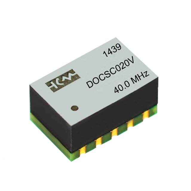
Surface Mount
Oven Stabilized Oscillator
DOCSC Series
www.digikey.com
OCXO or VCOCXO
2111 Comprehensive Drive
2111 Comprehensive Drive
Aurora, Illinois 60505
Aurora, Illinois 60505
Phone: 630- 851- 4722
Phone: 630- 851- 4722
Fax: 630- 851- 5040
Fax: 630- 851- 5040
www.conwin.com
www.conwin.com
Description:
Features:
Connor-Winfield’s high stability
DOCSC Series is an exceptionally
precise frequency standard, excellent
for use in cellular base stations, test
equipment, Synchronous Ethernet
and VSAT applications.
Based on an SC-cut crystal,
the DOCSC Series offers low aging and tight
stability in a 9x14mm surface mount package.
• OCXO or VCOCXO
• 3.3 Vdc Operation
• SMT Package
• Frequency Stability: ±20ppb or ±50ppb
• Temperature Ranges:
0 to 70°C, -20 to 75°C or -40 to 85°C
• Low Phase Noise
• LVCMOS Output
• RoHS Compliant / Lead Free
Suggested Pad Layout
Package Outline
Top
View
Side
View
0.085
(2.16mm)
0.060
(1.52mm)
4
0.100
(2.54mm)
DNC
Bottom
View
3
Top
5 View 2
0.260
(6.60mm)
0.100
(2.54mm)
0.040
(1.02mm)
0.025
(0.64mm)
0.375
(9.52mm)
0.085
(2.16mm)
DNC
0.275
(6.99mm)
1
0.555
(14.1mm)
0.060
(1.52mm)
0.330
(8.38mm)
1525
DOCSC022F
24.576MHz
0.358
(9.1mm)
0.040
(1.02mm)
6
1
DNC = Do Not Connect
Keep
Out
Area
Dimensional Tolerance: +/-0.005 (0.127mm)
Marking Diagram
Pad Connections
1: N/C or Voltage Control
2: Do Not Connect*
3: Ground
4: Output
5: Do Not Connect*
6: Supply Voltage (Vcc)
*DO NOT connect "DNC" pads
to ground or supply rails.
Ordering Information
Bulletin
Page
Revision
Date
Cx264
1 of 4
08
05 Oct 2021
DOCSC
02
0
F
Oscillator
Type
Frequency
Stability
Temperature
Range
Voltage Control
Option
3.3 Vdc
LVCMOS Output
Surface Mount
OCXO
02 = ±20 ppb
05 = ±50 ppb
0 = 0 to 70°C
1 = -20 to 75°C
2 = -40 to 85°C
F = OCXO
(Fixed Freq.)
V = VCOCXO
(Voltage Controlled)
-024.576M
Output
Frequency
* Number
of allowable
Frequency Format digits after
-xxx.xM Min *
the decimal
-xxx.xxxxxxM Max * point.
M = MHz
Attention: System Designers please review Application Note AN2093:
System Design Information and Printed Circuit Board Layout Guidelines for OCXO Oscillators.
@ www.conwin.com/technologies.html
�2111 Comprehensive Drive
Aurora, Illinois 60505
Phone: 630- 851- 4722
Fax: 630- 851- 5040
www.conwin.com
Absolute Maximum Ratings
Parameter
Minimum
Storage Temperature
Supply Voltage - 3.3 Vdc (Vcc)
Control Voltage (Vc)
Nominal
-55
-0.5
-0.5
-
-
-
Maximum
Units
Notes
125
4.5
Vcc+0.5
°C
Vdc
Vdc
Operating Specifications
Parameter
Center Frequency (Fo)
Frequency Stability vs. Change in Temperature
Option 02
Operating Temperature Range
Option 0
Option 1
Option 2
Frequency Calibration
Frequency Stability vs Load
Frequency Stability vs Voltage
Aging: Daily
Aging: First Year
Total Frequency Tolerance (20 Years)
Supply Voltage (Vcc)
Power Consumption Vcc = Nominal Voltage
Commercial Temperature Range: 0 to 70 °C
Turn On
Steady State @ 25°C
Industrial Temperature Range: -40 to 85 °C
Turn On
Steady State @ 25°C
Phase Jitter: (BW: 12 KHz to 5MHz @ Fo=40.0MHz)
Allan Deviation (Tau=1s)
Start-Up Time (for Vcc ramp < 500us)
Warm Up Time (Within Specification @ 25°C)
Warm Up Time (Within Specification @ -40°C)
Minimum
Nominal
Maximum
Units
Notes
-20
-
20
ppb
1
0
-20
-40
-1.0
-20
-20
-5.0
-0.3
-3.0
3.13
-
-
-
-
-
-
-
-
-
3.30
70
75
85
1.0
20
20
5.0
0.3
3.0
3.47
°C
°C
°C
ppm
ppb
ppb
ppb/day
ppm
ppm
Vdc
2
±5%
±5%
3
-
-
-
-
2.5
1.1
W
W
-
-
-
-
-
-
-
-
-
0.25
3.0E-11
-
-
-
3.0
1.3
0.35
10
60
90
W
W
ps RMS
ms
s
s
6
Notes
10
-
40
MHz
4
5
CMOS Output Characteristics
Parameter
Load
Output Voltage
Output Voltage: High (Voh)
Low (Vol)
Output Current: High (Ioh)
Low (Iol)
Duty Cycle at 50% of Vcc
Rise / Fall Time: 10% to 90%
Minimum
Nominal
Maximum
Units
2.7
-
-4
-
45
-
-
-
-
-
50
-
-
0.3
-
4
55
6.5
V
V
mA
mA
%
ns
-
15
-
pF
7
Typical Phase Noise Characteristics
Parameter
@ 1 Hz offset
@ 10 Hz offset
@ 100 Hz offset
@ 1 KHz offset
@ 10 KHz offset
@ 100 KHz offset
@ 1MHz offset
Fo=10 MHz
-72
-100
-128
-145
-151
-154
-155
Fo=24.576MHz
-70
-96
-125
-145
-151
-154
-155
Fo=40.0MHz
-67
-90
-116
-139
-147
-153
-153
Attention: System Designers please review Application Note AN2093:
System Design Information and Printed Circuit Board Layout Guidelines for OCXO Oscillators.
@ www.conwin.com/technologies.html
Units
dBC/Hz
dBC/Hz
dBC/Hz
dBC/Hz
dBC/Hz
dBC/Hz
dBC/Hz
Bulletin
Page
Revision
Date
Specifications subject to change without notification. See Connor-Winfield's website for latest revision.
© Copyright 2019 The Connor-Winfield Corporation Not intended for life support applications.
Notes
Cx264
2 of 4
08
05 Oct 2021
�2111 Comprehensive Drive
Aurora, Illinois 60505
Phone: 630- 851- 4722
Fax: 630- 851- 5040
www.conwin.com
Input Characteristics - Voltage Controlled Option
Parameter
Control Voltage Range:
Frequency Pullability:
Input Impedance
Linearity
Minimum
0.30
±3.0
100K
-
Nominal
1.65
-
-
-
Maximum
3.00
±10.0
-
±5
Units
V
ppm
Ohms
%
Notes
8
9
Package Characteristics
DOC Package
Package consisting of a FR-4 substrate and Ryton-R-4 cover. Water Resistant package,
non-hermetic seal. (Engineering Properties of Ryton R-4 Application Note AN2100)
Environmental Characteristics
Shock
500 G’s 1ms, Halfsine, 3 shocks per direction, per MIL-STD 202G, Method 213B Test Condition D.
Sinusoidal Vibration
0.06” D.A. or 10G’s Peak, 10 to 500 Hz, per MIL-STD-202G, Method 204D, Test Condition A.
Random Vibration
5.35 G’s rms. 20 to 2000 Hz per MIL-STD-202G, Method 214,Test Condition 1A, 15 minutes each axis.
Moisture
10 cycles, 95% RH, Per MIL-STD-202G, Method 112.
Marking Permanency
Per MIL-STD-202G, Method 215J.
Solder Process Recommendations:
RoHS compliant, lead free. See solder profile on page 4.
In-line reflow:
Refer to recommended reflow pre-heat and reflow temperatures on page 4. Package material
consist of Ryton R-4 high temperature cover with FR4 substrate. Component solder is Pb free high
temperature eutectic alloy with a melting point of 221°C.
In-line oven profile:
We recommend using KIC profiler or similar device placing one of the thermocouples on the
device to insure that the internal package temperature does not exceed 221°C.
Removal of device:
If for any reason the device needs to be removed from the board, use a temperature controlled
repair station with profile monitoring capabilities. Following a monitored profile will insure the
device is properly pre-heated prior to reflow. Refer to IPC 610E for inspection guidelines.
Recommended Cleaning Process: (If required)
Device is non-hermetic, water resistance with four weep holes, one in each corner to allow
moisture to be removed during the drying cycle. We recommend in-line warm water wash
with air knife and drying capabilities. If cleaner does not have drying capability, then use hot air
circulated oven. Boards should be placed in the oven vertically for good water runoff.
Device must be dried properly prior to use!
Note: If saponifier is used make sure the device is rinsed properly to insure all residues are removed. PH of saponifier should
not exceed 10.
Drying Temperature:
Between 85 to 100°C.
Drying Time:
Time will vary depending on the board size.
Caution: Do not submerge the device!
Notes:
1. Frequency stability vs. change in temperature. [±(Fmax - Fmin)/(2*Fo)].
2. Initial calibration @ 25°C. For OCXO with voltage control option, the control voltage must be fixed.
3. After 10 days of operation
4. Inclusive of calibration @ 25°C, frequency vs. change in temperature, change in supply voltage (±5%), load change (±5%), shock and vibration
and 20 years aging
5. Minimum "Power On Time" after rail rises from 0 to within +/-5% of Vcc = 1 second.
Supply voltage must reach Vcc level monotonically.
6. 10ms start time is guaranteed when supply voltage reaches Vcc level in less than or equal to 500us. If supply ramp is greater than 500us, then start
times as long as 1s are possible.
7. Attention: To achieve optimal frequency stability, and in some cases to meet the specification stated on this data sheet, it is required that the circuit
connected to this OCXO output must have the equivalent input capacitance that is specified by the nominal load capacitance. Deviations from the
nominal load capacitance will have a graduated effect on the stability of approximately 20 ppb per pF load difference.
8. Positive slope. (Frequency increases as Vc voltage increases). To ensure proper operation of VCOCXO's, the control voltage input must be biased
the nominal control voltage. Failure to bias the Vc input will cause an unstable output condition.
9. Referenced to Fo.
Attention: System Designers please review Application Note AN2093:
System Design Information and Printed Circuit Board Layout Guidelines for OCXO Oscillators.
@ www.conwin.com/technologies.html
Bulletin
Page
Revision
Date
Specifications subject to change without notification. See Connor-Winfield's website for latest revision.
© Copyright 2019 The Connor-Winfield Corporation Not intended for life support applications.
Cx264
3 of 4
08
05 Oct 2021
�2111 Comprehensive Drive
Aurora, Illinois 60505
Phone: 630- 851- 4722
Fax: 630- 851- 5040
www.conwin.com
Phase Noise Plot
Allan Deviation Plot
LVCMOS Test Circuit
RoHS Solder Profile
Temperature
DNC
10uF
to
100 uF
260°C
260°C
Output
220°C
180°C
0.01uF
150°C
2
DNC
Pad 1
VCOCXO = Vc
OCXO = NC
120°C
15 pF
DNC = Do Not Connect
DO NOT connect "DNC" pads
to ground or supply rails.
0
10 s
Up to 120 s
60 to 90 s
Typical
Typical
Meets IPC/JEDEC J-STD-020C
Tape and Reel Information
CMOS Output Waveform
1V/Div
SM-MECH51
Attention: System Designers please review Application Note AN2093:
System Design Information and Printed Circuit Board Layout Guidelines for OCXO Oscillators.
@ www.conwin.com/technologies.html
Bulletin
Page
Revision
Date
Specifications subject to change without notification. See Connor-Winfield's website for latest revision.
© Copyright 2019 The Connor-Winfield Corporation Not intended for life support applications.
Cx264
4 of 4
08
05 Oct 2021
�
很抱歉,暂时无法提供与“DOCSC022F-030.72M”相匹配的价格&库存,您可以联系我们找货
免费人工找货- 国内价格
- 1+474.55771
- 10+449.98734
- 国内价格
- 50+441.80719
- 100+425.44480


 工商网监
湘ICP备2023018690号
工商网监
湘ICP备2023018690号

