Available at Digi-Key
www.digikey.com
2111 Comprehensive Drive
Aurora, Illinois 60505
Phone: 630- 851- 4722
Fax: 630- 851- 5040
www.conwin.com
D
A
T
A
S
125 Series
FTS125-COO-010.0 MHz
GPS Disciplined Oscillators
General Description
The FTS125-COO-010.0 MHz frequency and time
standard module is an OCXO based GPS driven,
mixed-signal phase lock loop, providing a 1 PPS CMOS
output from a Connor-Winfield GPS timing receiver and
generating a 10 MHz CMOS and a 10 MHz SINE output
from an intrinsically low jitter voltage controlled crystal
oscillator. The FTS125 can lock to a 10 MHz reference
derived from the on-board GPS receiver or an external
10 MHz reference or to an external 1 PPS reference.
Alarms are provided to indicate Loss-of-Lock, Holdover,
and Antenna Fault. The on-board GPS receiver requires
an outdoor mounted GPS antenna for the best stability
and consistent performance.
The mode control inputs are used to manually
switch between references and/or holdover. The user
application should monitor the alarm outputs and
manually switch modes as needed.
Serial I/O lines provide access to the NMEA messages from the GPS receiver
(referenced in the Connor-Winfield’s Wi125 User Manual. Contact Connor-Winfield Sales
for a copy). The serial I/O lines can be used to access GPS timestamp information, or to
verify that the receiver has recovered from an alarm condition. The reset is used to reset
the GPS receiver (if needed).
H
Features
E
• 1 PPS output
• Phase locked 10 MHz output
• 3 selectable references: GPS, External 10 MHz or External 1 PPS
• Holdover
E
• Three alarm outputs. (Loss-of-Lock, Holdover and Antenna Fault)
• Serial input and output ports (GPS receiver)
T
• Master reset
• +3.3 Volt power supply
• Commercial Temp (0-70° C)
• Meets ITU-T G.811 Wander Generation Mask
• Meets ETSI-PRC Wander Generation Mask (with OCXO reference)
• MCX GPS Antenna Connection
• Fixed Position Unit
• Package: 32-pin Through-Hole
• Physical Dimensions: 4.15” x 3.3” x 0.718” (105.41mm x 83.82mm x 18.22mm)
Bulletin
Revision
Date
Issued By
SG184
02
03 Jan 12
ENG
�Functional Block Diagram
Figure 1
OCXO
or
TCXO
REFERENCE
FTS125 Module
SERIAL OUTPUT (A, B, C)
MCX
Connector
BOOT SEL
HOLDOVER STATUS
LOCK STATUS
ANTENNNA FAULT STATUS
Wi125
(GPS Receiver)
1 PPS CMOS OUTPUT
SERIAL IN
(A, B, C)
33Ω
1 PPS
∆
GPS REF
10 MHz REF
DPFD
1 PPS REF
RESET
SYNC 1 CONTROL
SYNC 2 CONTROL
CPLD
ANALOG
FILTER
LOW JITTER
VCXO
or
OCVCXO
1/N
DRIVER
33Ω
DISABLE
JTAG
(Programming Only)
DRIVER
&
TRANSLATION
FTS125-COO Data Sheet #: SG184
Page 2
10 MHz CMOS
OUTPUT
10 MHz SINE
OUTPUT
Rev: 02
Date: 01/03/12
© Copyright 2012 The Connor-Winfield Corp. All Rights Reserved Specifications subject to change without notice
�Typical Application
Figure 2
FTS125-COO Data Sheet #: SG184
Page 3
Rev: 02
Date: 01/03/12
© Copyright 2012 The Connor-Winfield Corp. All Rights Reserved Specifications subject to change without notice
�Pin Description
Table 1
Pin #
Pin Name
Description
1
TXC
RS-232 communication transmit signal for UART2 (Optional)
2
TXB
RS-232 communication transmit signal for UART1 (Optional)
3
TXA
RS-232 communication transmit signal for UART0 (Optional)
4
GND
5
RXC
RS-232 communication receive signal for UART2 (Optional)
6
RXB
RS-232 communication receive signal for UART1 (Optional)
7
RXA
RS-232 communication receive signal for UART0 (Optional)
8
*Bootsel
9
10 MHz Ref Input
External LVCMOS 10 MHz reference (Optional). Default state is pulled high internally.
10
*Reset
Hardware Reset for the GPS timing circuitry. Pull low to reset. Default state is pulled
high internally.
11
GND
12
1 PPS Ref Input
13
GND
14
Antenna Supply Voltage
15
GND
16
VCC1
Supply voltage for GPS timing circuitry.
17
VCC2
Supply voltage for noise clean-up and interfacing circuitry.
18
GND
19
SYNC1 Control
Lock mode control signal 1. See Table 4 for functional description.
Default state is pulled high internally.
20
SYNC2 Control
Lock mode control signal 2. See Table 4 for functional description.
Default state is pulled high internally.
21
*Disable
22
Unused
23
Holdover Status
24
Lock Status
25
Antenna Fault Status
High= A fault has been detected on Pin 14 (Antenna Supply Voltage)
26
1 PPS CMOS Output
1 PPS CMOS output provided by the Wi125
27
GND
28
10 MHz CMOS Output
29
Unused
30
Unused
31
GND
32
10 MHz SINE Output
Normally HIGH - Only pulled low for RS-232 re-programming of GPS software.
Default state is pulled high internally.
External LVCMOS 1 PPS reference (Optional). Default state is pulled high internally.
Antenna Supply Voltage. Limit continuous current to 45mA Max.
Open/High = enabled outputs. Pull low to disable the 10MHz CMOS and SINE outputs.
Default state is pulled high internally.
High= Unit is in Holdover
High= Unit is locked to selected reference.
10 MHz low jitter CMOS output
10 MHz AC coupled low jitter SINE output
FTS125-COO Data Sheet #: SG184
Page 4
Rev: 02
Date: 01/03/12
© Copyright 2012 The Connor-Winfield Corp. All Rights Reserved Specifications subject to change without notice
�Absolute Maximum Rating
Table 2
Symbol
Parameter
Minimum
Maximum
Units
N otes
VCC
Power Supply Voltage
-0.3
3.7
Volts
1
VIN
Input Voltage
-0.3
4.6
Volts
1
VPREAMP
Antenna Supply Voltage
2.7
13.2
Volts
1
TS
Storage Temperature
-30
80
°C
1
Operating Specifications
Table 3
Symbol
Parameter
VCC1
Supply Voltage 1
ICC1
Supply Current 1
VCC2
Supply Voltage 2
ICC2
Supply Current 2
TO
Temperature Range
tJTOL
Input Jitter Tolerance
tAQ_GPS
GPS Input Acquisition Time
150
sec
3
tAQ_EXT
External Input Acquisition Time
120
sec
3
Oscillator Performance
FCAP
Capture/Pull-in Range
Minimum
Nominal
Maximum
3.135
3.3
3.465
V
.480
1.2
A
3.135
3.3
3.465
V
.380
1.0
A
0
70
°C
30
±45 ppb
FBW
Jitter Filter Bandwidth
0.1 Hz Typ.
DC
Duty Cycle
45/55%
RMS
RMS Phase Noise
10 Hz - 2 MHz
12 kHz - 2 MHz
1 ps Typ.
0.6 ps Typ
Units
Vcc Stability
ADAILY
Daily Aging
2 ppb
AYEARLY
Yearly Aging
80 ppb
Wander Generation Specification
ETSI-PRC
2
ns
Holdover/Wander Generation Performance
TSTA
Temperature Stability
±20 ppb
VSTA
Notes
4
5
±5 ppb
NOTES:
1. Stresses beyond those listed under “Absolute Maximum Rating” may cause permanent damage to the module. These are stress ratings only and functional operation of the device at these or any other
conditions beyond those indicated under “Operating Specifications” is not implied. Exposure to absolute maximum rated conditions for extended periods may affect device reliability.
2. Requires external regulation and supply decoupling.
3. Cold Power-up.
4. Holdover will be re-calculated with each successful lock. Yearly aging represents 1 continuous year in Holdover.
5. Relative to 25°C.
FTS125-COO Data Sheet #: SG184
Page 5
Rev: 02
Date: 01/03/12
© Copyright 2012 The Connor-Winfield Corp. All Rights Reserved Specifications subject to change without notice
�Mode Control Table
Table 4
* Note: Holdover is not supported in this mode; loss of the 10MHz reference will rail the
PLL output until the reference returns or another mode is selected.
Input And Output Characteristics
Table 5
LVCMOS Inputs and Outputs
Minimum
Maximum
Symbol
Parameter
Units
VIH
High Level Input Voltage
1.7
4.0
V
VIL
Low Level Input Voltage
-0.5
0.8
V
VOH
High Level Output Voltage
2.4
V
VOL
Low Level Output Voltage
0.4
V
CO
Output Capacitance
10
pF
Symbol
Parameter
Load
50
ohms
Output Power
9
dBm
Total Harmonic Distortion
2.2
%
Notes
10MHz Sine Output
Typical
Units
Notes
GPS Receiver Specifications
Table 6
Parameter
Specifications
Acquisition/Tracking Sensitivity
-155dBm/-156dBm
Notes
Acquisition Time:
Hot Start w/ Network Assist Outdoor:
很抱歉,暂时无法提供与“FTS125-COO-010.0M”相匹配的价格&库存,您可以联系我们找货
免费人工找货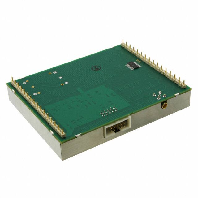


 工商网监
湘ICP备2023018690号
工商网监
湘ICP备2023018690号
