Available at Digi-Key
www.digikey.com
2111 Comprehensive Drive
Aurora, Illinois 60505
Phone: 630- 851- 4722
Fax: 630- 851- 5040
www.conwin.com
D
A
T
A
S
H
E
FTS250-HP GPS
Disciplined Oscillator
Connor-Winfield’s GPS Disciplined
Oscillators (GPSDOs) were created specifically for
precision timing, synchronization and time stamping
applications requiring high end, cost sensitive
solutions. By combining our uniquely designed
phase lock loop circuitry, a GPS/GNSS receiver and
our high-quality oscillators, Connor Winfield is able
to offer a wide variety of superior, cost-effective GPS
timing solutions. The FTS250-HP Series modules
provide customer applications with the precise timing
capabilities needed to optimize critical system performance.
General Description
The FTS250-HP-010.0M Frequency and Time Standard module is a GPS/GNNS driven, mixed-signal
phase lock loop, providing a 1 PPS CMOS output from an onboard GPS/GNSS timing receiver. The
FTS250-HP generates a 10 MHz CMOS and a 10 MHz SINE output from an intrinsically low jitter
voltage controlled crystal oscillator. The FTS250-HP locks to a 1 PPS reference derived from the onboard GPS receiver from which It generates the 10MHz outputs and the 1PPS output.
The module can also be programmed to lock to an external 10 MHz reference or to an external 1 PPS
reference. Alarms are provided to indicate Loss-of-Lock, Holdover, and Antenna Fault status. The onboard GPS receiver requires an outdoor mounted GPS antenna for the best stability and consistent
performance.The mode control inputs are used to manually switch between references and/or holdover.
The user application should monitor the alarm outputs and manually switch modes as needed.
Serial I/O lines provide access to the NMEA messages from the GPS receiver. The serial I/O lines can
be used to access GPS timestamp information, or to verify that the receiver has recovered from an
alarm condition. The reset is used to reset the GPS receiver (if needed).
Features
E
• Phase locked 10 MHz output (other frequencies available upon request)
T
• Multiple Holdover Thermal Stability Options
• Phase locked 1 PPS output
• Three selectable references: GPS, External 10 MHz or External 1 PPS
• Three alarm outputs. (Loss-of-Lock, Holdover and Antenna Fault)
• Serial input and output ports (GPS receiver)
• Master reset
• +3.3 Volt power supply
• Temperature Range: -40°C to 85°C
• Meets ITU-T G.811 Wander Generation Mask
• SMA Bulkhead GPS Antenna Connection
• Package: 28-pin Through-Hole
• Physical Dimensions: 2.8” x 1.725” x 0.368” (71mm x 43.82mm x 9.34mm)
• Fixed Position
Bulletin
Revision
Date
SG176
04
03 July 2019
• Multiple Output Frequency Options in addition to 10MHz.
�Functional Block Diagram
Figure 1
FTS250 Module
SERIAL OUTPUT
SMA Bulkhead
Connector
HOLDOVER STATUS
LOCK STATUS
ANTENNNA FAULT STATUS
LEA-M8F
1 PPS CMOS OUTPUT
(GPS Receiver)
SERIAL IN
1 PPS
GPS REF
NS2000-1PPS
10 MHz REF
DPLL
1 PPS REF
RESET
SYNC 1 CONTROL
SYNC 2 CONTROL
DISABLE
Micro
Controller
ANALOG
PLL
DRIVER
10 MHz CMOS
OUTPUT
10 MHz SINE
OUTPUT
Pin Description
Table 1
1
2
3
4
5
6
7
8
9
10
11
12
13
14
15
16
17
18
19
20
21
22
23
24
25
26
27
28
33Ω
DRIVER
&
TRANSLATION
TCXO
or OCXO MCLK
VCXO
Phase Control
NCO Adjust
1PPS Pulse
Generator
BOOT SEL
Pin #
LOW JITTER
Pin Name
Vcc2
GND
*Reset
*Disable
1 PPS Ref Input
GND
10 MHz Ref Input
NU
NU
NU
NU
*Bootsel
GND
Vcc1
Antenna Supply Voltage
GND
RXA
TXA
SYNC2 Control
SYNC1 Control
Lock Status
Holdover Status
Antenna Fault Status
1 PPS CMOS Output
GND
10 MHz CMOS Output
GND
10 MHz SINE Output
Description
Note
3.3V ±5% Supply Voltage
Hardware Reset for GPS Circuitry. Pull low to Reset
Open/High = Enabled Outputs. Low = Disabled Outputs
External 1 PPS reference
1
1
1
External LVCMOS 10 MHz Reference
Used for Factory Programming
Used for Factory Programming
Used for Factory Programming
Used for Factory Programming
Normally High - Pulled low during Wi125 software updates
1
3.3V ±5% Supply Voltage
2.7 to 13.2V Input Supply Voltage for the Antenna. Max 45mA continuous current
2
RS-232 Communication receive signal for UART-0
RS-232 Communication transmit signal for UART-0
Lock mode selection control signal 2
Lock mode selection control signal 1
High = Unit is locked to the selected reference
High = Unit is in Holdover
High = Fault detected on the Antenna Supply Voltage (Self Clearing)
1 PPS LVCMOS Output
10 MHz LVCMOS Output (Defalt)
1
1
1
1
1
1
1, 3
10 MHz Sine Output (~9dBm)
Note: 1. 3.3 VDC (LVCMOS) compatible
2. If OCXO option is chosen, must add OCXO current to this base current.
FTS250-HP Data Sheet #: SG176
Page 2
Rev: 04
Date: 07/03/19
Specifications subject to change without notification. See Connor-Winfield’s website for latest revision.
© Copyright 2019 The Connor-Winfield Corporation Not intended for life support applications.
�Absolute Maximum Rating
Table 2
Symbol
Parameter
Minimum
Maximum
Units
N otes
VCC
Power Supply Voltage
-0.3
3.7
Volts
1
VIN
Input Voltage
-0.3
4.6
Volts
1
VPREAMP
Antenna Supply Voltage
2.7
13.2
Volts
1
TS
Storage Temperature
-40
85
°C
1
Operating Specifications
Table 3
Symbol
Parameter
Minimum
VCC1
Supply Voltage 1
3.135
ICC1
Supply Current 1
VCC2
Supply Voltage 2
3.135
ICC2
Supply Current 2
TO
Temperature Range
-40
tJTOL
Input Jitter Tolerance
30
ns
tAQ_GPS
GPS Input Acquisition Time
100
sec
3
tAQ_EXT
External Input Acquisition Time
100
sec
3
FCAP
Capture/Pull-in Range
Nominal
3.3
Maximum
Units
Notes
3.465
V
2
A
0.270
3.465
V
0.036
3.3
A
85
°C
O
scillator Performance
Dependent upon holdover option chosen
ppm
FBW
Jitter Filter Bandwidth
0.8
Hz
DC
Duty Cycle
45/55
%
RMS
RMS Phase Noise
10 Hz - 2 MHz
12 kHz - 2 MHz
1.2
0.6
ps
Holdover/Wander Generation Performance
Frequency Stability
Wander Generation Specification
2
See Holdover Specification Options
ppm
4
5
ITU-T G.811
NOTES:
1. Stresses beyond those listed under “Absolute Maximum Rating” may cause permanent damage to the module. These are stress ratings only and
functional operation of the device at these or any other conditions beyond those indicated under “Operating Specifications” is not implied. Exposure
to absolute maximum rated conditions for extended periods may affect device reliability.
2. Requires external regulation and supply decoupling.
3. Cold Power-up.
4. Holdover will be re-calculated with each successful lock. Yearly aging represents 1 continuous year in Holdover.
5. Includes unidirectional temperature stability, Vcc stability, and 24 hours of aging.
FTS250-HP Data Sheet #: SG176
Page 3
Rev: 04
Specifications subject to change without notification. See Connor-Winfield’s website for latest revision.
© Copyright 2019 The Connor-Winfield Corporation Not intended for life support applications.
Date: 07/03/19
�Mode Control Table
Table 4
SYNC 1
0
0
1
1
SYNC 2
0
1
0
1
Operating Mode
Force Holdover
Lock to External 10 MHz reference*
Lock to External 1 PPS reference
(Default) Lock to GPS Signal
* Note: Holdover is not supported in this mode; loss of the 10MHz reference will rail the
PLL output until the reference returns or another mode is selected.
Input And Output Characteristics
Table 5
LVCMOS Inputs and Outputs
Minimum
Maximum
Symbol
Parameter
VIH
High Level Input Voltage
1.7
4.0
Units
VIL
Low Level Input Voltage
-0.5
0.8
V
VOH
High Level Output Voltage
2.4
V
VOL
Low Level Output Voltage
0.4
V
CO
Output Capacitance
10
pF
Symbol
Parameter
Load
50
ohms
Output Power
Total Harmonic Distortion
9
2.2
dBm
%
10 MHz Sine Output
Typical
Table 6
Units
Notes
GPS Receiver Specifications
Parameter
Specifications
Time to First Fix:
Cold:
Aided Cold Start
Timing Fix:
29 sec
很抱歉,暂时无法提供与“FTS250-010.0M”相匹配的价格&库存,您可以联系我们找货
免费人工找货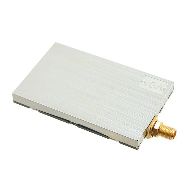


 工商网监
湘ICP备2023018690号
工商网监
湘ICP备2023018690号
