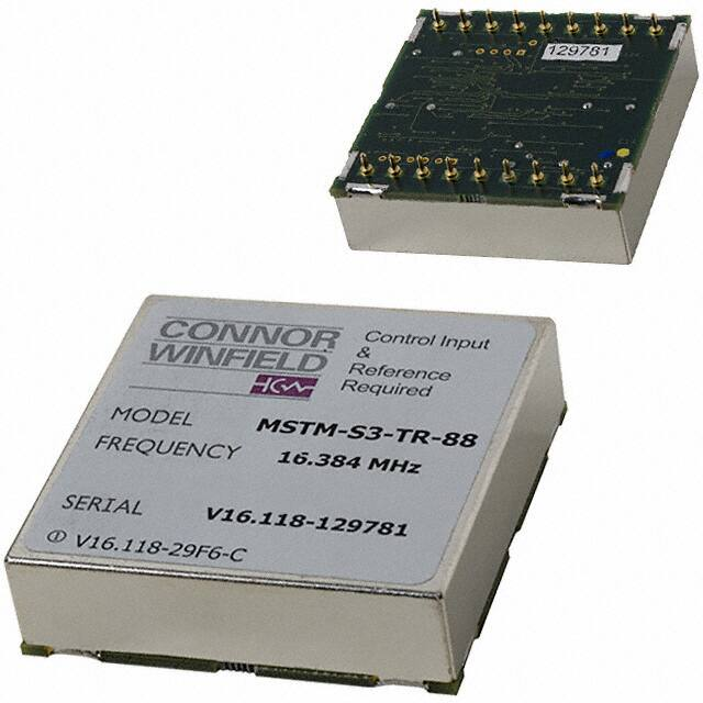
MSTM-S3-TR
Stratum 3
Timing Module
2111 Comprehensive Drive
Aurora, Illinois 60505
Phone: 630- 851- 4722
Fax: 630- 851- 5040
www.conwin.com
Bulletin
Page
Revision
Date
Issued By
TM027
1 of 16
P05
02 DEC 02
MBatts
Application
Features
The Connor-Winfield MSTM-S3-TR
Simplified Control Timing Module acts as a
complete system clock module for Stratum 3
timing applications in accordance with GR1244, Issue 2 and GR-253, Issue 3.
Connor Winfield’s Stratum 3 timing modules
helps reduce the cost of your design by
minimizing your development time and
maximizing your control of the system clock
with our simplified design.
• 5V Miniature Timing
Module
• Redundant
References
• 2 Synchronous
Outputs Available
From 8 kHz to
77.76MHz
• 40 sec., Filtered,
Hold Over History
• Operational Status
Flags
�General Description
Functional Block Diagram
The Connor-Winfield Stratum 3 Simplified Control Timing Module acts as a complete system clock module for general Stratum
3 timing applications. The MSTM is designed to replace similar
units from TF Systems (TF118B) and Raltron (SY0001B).
Full external control input allows for selection and monitoring
of any of four possible operating states: 1) Holdover, 2) External
Reference #1, 3) External Reference #2, and 4) Free Run. Table
#1 illustrates the control signal inputs and corresponding operational states.
In the absence of External Control Inputs (A,B), the MSTM
enters the Free Run mode and signals an External Alarm. The
MSTM will enter other operating modes upon application of a
proper control signal. Mode 1 operation (A=1, B=0) results in an
output signal that is phase locked to the External Reference
Input #1. Mode 2 operation (A=0, B=1) results in an output signal that is phase locked to External Reference Input #2. Holdover mode operation (A=1, B=1) results in an output signal at or
near the frequency as determined by the latest (last) lockedsignal input values and the holdover performance of the MSTM.
Free Run ModeFree Run mode operation (A=0, B=0) is a guaranteed output of 4.6 ppm of the nominal frequency.
Alarm signals are generated at the Alarm Output during Holdover and Free Run operation. Alarm Signals are also generated
by Loss-of-Lock and Loss-of-Reference conditions. A high level
indicates an alarm condition. Real-time indication of the operational mode is available at unique operating mode outputs on
pins 1-4.
Control loop 0.1 Hz filters effectively attenuate any reference
jitter, smooth out phase transients, comply with wander transfer
and jitter tolerances.
Figure 1
1
Free Run
CNTL A
2
Ref #1
CNTL B
3
Ref #2
4
Hold Over
Free Run
PLL_TVL
Hold Over
Tuning
Voltage
Monitor
Ex Ref 1
Ref
Control
Ex Ref 2
Alarm_Out
Holdover
FIFO
LOL & LOR
Phase
Build Out
Circuit
DPLL
DAC
Stratum3
OCXO
Sync_Out
÷N
Opt_Out*
Reference
Clock
*Only one Opt_Out option is available per module
Function Control Table
Table 1
CNTL
A
CNTL
B
Operational
Mode
0
0
1
0
External
Reference
#1
0
1
External
Reference
#2
1
1
Ref 1
Free Run (Default Mode)
Ref 2
Hold Over
Free Run
PLL Unlock
Alarm Out
0
0
0
1
0
1
Normal
PLL_Unlock
LOR
1
1
0
0
0
0
0
0
1
0
0
0
0
1
0
0
0
1
Normal
PLL_Unlock
LOR
0
0
0
1
1
0
0
0
1
0
0
0
0
1
0
0
0
1
0
0
1
0
0
1
Hold Over
Absolute Maximum Rating
Table 2
Symbol
Parameter
Minimum
Maximum
Units
Notes
VCC
Power Supply Voltage
-0.5
Nominal
7.0
Volts
1.0
VI
Input Voltage
-0.5
VCC + 0.5
Volts
1.0
Ts
Storage Temperature
-55
100
deg. C
1.0
Data Sheet #: TM027
Page 2 of 16
Rev: P05
Date: 12 / 02 / 02
© Copyright 2001 The Connor-Winfield Corp. All Rights Reserved Specifications subject to change without notice
�Recommended Operating Conditions
Table 3
Symbol
Parameter
Minimum
Nominal
Maximum
Units
Vcc
Power supply voltage
4.75
5.00
5.25
Volts
VTH
Reset threshold voltage
4.25
4.5
Volts
VIH
High level input voltage - TTL
2.0
VCC
Volts
VIL
Low level input voltage - TTL
0
tIN
Input signal transition - TTL
CIN
Input capacitance
VOH
High level output voltage,
IOH = -4.0mA, VCC = min.
VOL
Low level output voltage,
IOL = 12.0 mA, VCC = min.
tTRANS
Clock output transition time
tPULSE
8kHz input reference pulse
width( positive or negative)
30
TOP
Operating temperature
0
2.4
0.8
Volts
250
ns
15
pF
5.25
Volts
0.4
Volts
4.0
Notes
2.0
ns
ns
70
°C
Specifications
Table 4
Parameter
Specifications
Frequency Range (Sync_Out)
8 kHz to 77.76 MHz
Notes
Frequency Range (Opt_Out)
8 kHz to 77.76 MHz
Supply Current
250 mA typical, 400 mA during warm-up (Maximum)
Timing Reference Inputs
8 kHz - 19.44 MHz
Jitter, Wander and Phase Transient Tolerances
GR-1244-CORE 4.2-4.4, GR-253-CORE 5.4.4.3.6
3.0
Wander Generation
GR-1244-CORE 5.3, GR-253-CORE 5.4.4.3.2
Wander Transfer
GR-1244-CORE 5.4
Jitter Generation
GR-1244-CORE 5.5, GR-253-CORE 5.6.2.3
Jitter Transfer
GR-1244-CORE 5.5, GR-253-CORE 5.6.2.1
Phase Transients
GR-1244-CORE 5.6, GR-253-CORE 5.4.4.3.3
Free Run Accuracy
4.6 ppm over TOP
Hold Over Stability
±0.37 ppm for initial 24 hrs
Inital Offset
±0.05 ppm
Temperature
±0.28 ppm
Drift
±0.04 ppm
Maximum Hold Over History
40 seconds
Pull-in/ Hold-in Range
±13.8 ppm minimum
Lock Time
30 seconds typical
DPLL Bandwidth
< 0.1 Hz
NOTES:
1.0: Stresses beyond those listed under Absolute Maximum Rating may cause damage
to the device. Operation beyond Recommended Conditions is not implied.
4.0:
2.0:
Logic is 3.3V CMOS
5.0:
3.0
GR-1244-CORE 3.2.1
4.0
5.0
Hold Over stability is the cumulative fractional frequency offset as described by
GR-1244-CORE, 5.2
Pull-in Range is the maximum frequency deviation from nominal clock rate on the
reference inputs to the timing module that can be overcome to pull into synchronization
with the reference
Data Sheet #: TM027
© Copyright 2001 The Connor-Winfield Corp.
Page 3 of 16
Rev: P05
Date: 12 / 02 / 02
All Rights Reserved Specifications subject to change without notice
�Pin Description
Table 5
Pin #
Connection
Description
1
Hold Over
Indicator output. High output when Hold Over mode is selected by control pins.
2
Ref 1
Indicator output. High output when Ref 1 mode is selected by control pins.
3
Ref 2
Indicator output. High output when Ref 2 mode is selected by control pins.
4
Free Run
Indicator output. High output when Free Run mode is selected by control pins.
5
GND
Ground
6
Alarm _Out
Alarm output. High output if module is in Free Run, or Hold Over, or LOR.
7
CNTL A
Mode control input
8
CNTL B
Mode control input
9
PLL_Unlock
Indicates that the PLL is not locked to a reference.
10
Tri-State/GND
0 = Normal operation, 1= Tri-State. Pin is pulled low internally.
Ground pin for normal operation.
11
Sync_Out
Primary timing output signal. Signal is sychronized to reference.
12
GND
Ground
13
Opt_Out
Secondary output signal. Signal is derived from Sync_Out or from an internal
reference clock depending upon the choosen configuration.
14
GND
Ground
15
Ex_Ref_2
External Input Reference #2
16
GND
Ground
17
Ex_Ref_1
External Input Reference #1
18
Vcc
+5V dc supply
Ordering Information
MSTM-S3-TR-(Input Reference Frequency)(Opt_Out Frequency)-(Primary Output)
1= 1.544 MHz
2= 2.048 MHz
8= 8 kHz
9= 19.44 MHz
S= Other
Primary Output ÷ N option:
2= 2.048 MHz
8= 8 kHz
N= No output
S= Other
Reference Clock Out option:
6= 16.384 MHz
9= 19.44 MHz
02.048M = 2.048MHz
016.384M = 16.384 MHz
019.44M = 19.44 MHz
032.768M = 32.768 MHz
038.88 M = 38.88 MHz
077.76 M = 77.76 MHz
Example: MSTM-S3-TR-88-038.88M
Data Sheet #: TM027
Page 4 of 16
Rev: P05
Date: 12 / 02 / 02
© Copyright 2001 The Connor-Winfield Corp. All Rights Reserved Specifications subject to change without notice
�Typical Application
Figure 2
BITS
System
Signal
Input Select
Line Card 1
S
A
CW’s SCG
2000/4000
MUX
A
MUX
B
B
CW’s STM/MSTM module
Y
Y
Clock out
S
RCV
Line Card N
Timing Card #N
S
A
A
MUX
B
MUX
CW’s STM/MSTM module
Y
B
CW’s SCG
2000/4000
Y
Clock out
RCV
S
System Select
Typical System Test Set-up
Figure 3
G P S or LO R AN
T im in g S o u r c e
T h is d e v ic e s u p p lie s s y s te m tim e
in f o r m a t io n . It c a n b e th o u g h t o f a s
s u p p ly in g " a b s o lu te tim e " r e fe r e n c e
in f o r m a t io n
S a m p le M T IE D a t a fo r S T M -S 3 /M S T M - S 3
1 .0 E - 6
P o s s ib le C h o i c e s In c lu d e
S ta n fo r d R e s e a r c h M o d e l: F S 7 0 0
T r u e tim e M o d e l X X X
T y p i c a l r e s p o n s e - 3 0 0 0 s e c o n d t e s t - J it t e r a p p li e d ( 2 U I @
re f d a t e A P R
1 0 H z)
2 2 1 99 8
k dh
M T IE (s
1 0 0 .0 E - 9
10
MHz
M T IE
1 0 .0 E - 9
1 2 4 4 - 5 .2 M a s k ( A )
1 2 4 4 - 5 .2 M a s k ( B )
1 2 4 4 - 5 .6 M a s k
G R 2 5 3 - 5 . 4 . 4 .3 . 2
1 .0 E - 9
1 0 0 .0 E - 3
1 .0 E + 0
1 0 .0 E + 0
1 0 0 .0 E + 0
O b s e r v a t io n T im e ( s )
1 .0 E + 3
C o p y ri g h t
1 0 .0 E + 3
1 9 9 8 C o n n o r - W in f i e ld a l l r i g h t s re s e r v e d
T a rg e t S y s te m U n d e r T e s t
C lo c k o r B IT S lo g ic le v e l
c lo c k in p u t ( T T L , C M O S ,
e tc .)
A r b it r a r y
W a v e fo r m
G e n e ra to r
[N o is e
S o u rc e ]
S a m p le W a n d e r G e n e r a t io n (T D E V ) f o r S T M /M S T M - S 3
1 .0 E - 6
T y p i c a l r e s p o n s e - 3 0 0 0 s e c o n d te s t - J itt e r a p p l ie d ( 2 U I @
re f d a te A P R
10 H z)
2 2 1 99 8
k dh
1 0 0 .0 E - 9
1 0 .0 E - 9
TDE V (s e c
DS-1 Line Card
OC-48 Line Card
OC-3 Line Card
. . . . ...
OC-12 Line Card
M T IE , T D E V , W a n d e r T r a n s f e r ,
a n d W a n d e r G e n e r a t io n P l o t s
Line Card
Noise Modulation Input
10
MHz
E x te r n a l
R e fe re n c e
In p u t
S ta n d a r d s
C o m p lia n c e
D o c u m e n ts
D S 1 r a te R Z ( 1 .5 4 4 M H z ) , E 1 r a te R Z o r 8 k H z
c lo c k R Z w ith n o is e m o d u la tio n
Timing Card
A r b it r a r y
W a v e fo r m
G e n e ra to r
Timing Card
E x te r n a l
R e fe re n c e
In p u t
T D EV
G R 1 2 4 4 - F ig 5 . 1
1 .0 E - 9
G R 1 2 4 4 - F ig 5 - 3
1 0 0 .0 E - 1 2
1 0 .0 E - 3
1 0 0 .0 E - 3
1 .0 E + 0
In te g r a t io n
(s e c )
1 0 0 .0 E + 0
1 .0 E + 3
C o p y r i g h t 1 9 9 8 C o n n o r - W i n f ie l d a ll l rig h t s r e s e r v e d
T im e - s ta m p e d e n s e m b le
b a s e d o n a b s o lu te tim e
r e fe r e n c e ( 1 0 M H z in p u t)
10
MHz
D S 1 r a te [1 .5 4 4 M H z ] B IT S B ip o la r
1 0 .0 E + 0
T im e
P h a s e E r r o r d a ta o u t p u t
D S - 1 , O C - 3 , O C - 1 2 e le c tr ic a l o r o p tic a l s ig n a ls
10
MHz
T e k tr o n ix
S J300E
E x te r n a l
R e fe re n c e
In p u t
HP 53310A
M o d u la tio n A n a ly z e r / T im e I n te r v a l A n a ly z e r
W a n d e r A n a ly z e r d a ta ( IE E E - 4 8 8 )
E x te r n a l
R e fe re n c e
In p u t
IE E E - 4 8 8 C o n tr o lle r
P la t f o r m f o r s o f tw a r e
H P 5 3 3 0 5 A P h a s e A n a ly z e r
H P E 1748A S ync
M e a s u re m e n t
T e k t r o n ix W a n d e r A n a ly z e r
T E K T R O N IX S J 3 0 0 E
Data Sheet #: TM027
© Copyright 2001 The Connor-Winfield Corp.
Page 5 of 16
Rev: P05
Date: 12 / 02 / 02
All Rights Reserved Specifications subject to change without notice
�MSTM-S3-TR Typical Current Draw
Figure 4
TYPICAL CURRENT DRAW
STS/MSTS-S3-T2
0.45
CURRENT (A)
0.4
0.35
0.3
0.25
0.2
0.15
0.1
0.05
0
0
10
20
30
40
50
60
TIME (Sec)
Typical Calibrated Wander Transfer TDEV
Figure 5
10000
100
TDEV (ns)
GR1244, Fig 5.3
10
10000
1000
100
10
1
0.1
1
0.01
TDEV (ns)
1000
Integration Time (Sec.)
Data Sheet #: TM027
Page 6 of 16
Rev: P05
Date: 12 / 02 / 02
© Copyright 2001 The Connor-Winfield Corp. All Rights Reserved Specifications subject to change without notice
�Typical Wander Generation MTIE
Figure 6
1000
G R 1 2 4 4 , F ig 5 .2 (A )
G R 1 2 4 4 , F ig 5 .2 (B )
G R 2 5 3 -5 .4 .4 .3 .2 , F ig 5 .1 7
MTIE (ns)
M T IE (n s )
100
1000000
100000
10000
1000
100
10
1
0.1
10
O b s e r v a tio n T im e (s e c .)
Typical Wander Generation TDEV
Figure 7
100
T D E V (n s)
G R 1244, F ig 5.1
TDEV (ns)
10
1
10000
1000
100
10
1
0.1
0 .1
In te g ra tio n T im e (s e c .)
Data Sheet #: TM027
© Copyright 2001 The Connor-Winfield Corp.
Page 7 of 16
Rev: P05
Date: 12 / 02 / 02
All Rights Reserved Specifications subject to change without notice
�1µ
µs Phase Transient TIE
Figure 8
1200
1000
TIE (ns)
800
600
400
200
0
-200
0
1
2
3
4
5
6
7
8
9
10
Time (sec)
Typical Phase Transient MTIE
Figure 9
10000
MTIE (ns)
1000
G R -2 5 3 , F i g . 5 -1 9 , R e q u i r e m e n t
M T I E (n s)
100
10
1
0 .0 1
0 .1
1
10
100
1000
O b s e rv a tio n T im e (s e c )
Data Sheet #: TM027
Page 8 of 16
Rev: P05
Date: 12 / 02 / 02
© Copyright 2001 The Connor-Winfield Corp. All Rights Reserved Specifications subject to change without notice
�Entry Into Hold Over
Figure 10
10000
MTIE (ns)
1000
100
G R -1 2 4 4 O b je c tive , F ig . 5 -8
G R -1 2 4 4 R e q ui re m e nt, F ig . 5 -8
G R -2 5 3 , F ig . 5 -1 9 , R e q uire m e nt
T yp ic a l M T IE
10
1
0 .0 0 1
0 .0 1
0 .1
1
10
100
1000
O b s e rv a tio n T im e (s e c o n d s )
Return from Hold Over
Figure 11
10000
MTIE (ns)
1000
100
G R -1 2 4 4 R e q u ire m e n t , F ig . 5 -7
G R -2 5 3 , F ig . 5 -1 9 , R e q u ire m e n t
Ty p ic a l M TIE
10
1
0.001
0.01
0.1
1
10
100
1000
O b se r v a ti o n T i m e (se c . )
Data Sheet #: TM027
© Copyright 2001 The Connor-Winfield Corp.
Page 9 of 16
Rev: P05
Date: 12 / 02 / 02
All Rights Reserved Specifications subject to change without notice
�MSTM-S3-TR Mode Indicator Delay
Figure 12
Change in
Operational Mode
Operational Mode
Indicator
∆tm
10
usec


 工商网监
湘ICP备2023018690号
工商网监
湘ICP备2023018690号
