Available at Digi-Key
www.digikey.com
OX200-SC
10 MHz VCOCXO
CO-8 Package
Features:
Description:
2111 Comprehensive Drive
37
Fax: 630- 851- 5040
www.conwin.com
12
Phone: 630- 851- 4722
SC
0- z
20 MH
OX .0
12
10
90
78
56
34
12
Aurora, Illinois 60505
Connor-Winfield model OX200-SC
is a 12 Vdc, Oven Compensated
Crystal Oscillator with Voltage
Control Option (VCOCXO) in a
CO-8 package. The OX200-SC is
designed for use with applications
that require a LVCMOS output, very
high frequency stability, low jitter
and low phase noise.
• VCOCXO
• 12 Vdc Operation
• CO-8 Footprint
• Frequency Stability: ±1.5 ppb
• Temperature Range: 0 to 70°C
• LVMOS Output
• Low Jitter and Phase Noise
• RoHS Compliant / Lead Free
Absolute Maximum Ratings
Parameter
Storage Temperature
Operable Temperature Range:
Supply Voltage (Vcc)
Output Load
Minimum
-55
-55
-
-
Nominal
-
-
-
-
Maximum
125
85
15
50
Units
Notes
°C
°C
Vdc
pF
CMOS Signal
Units
Notes
Frequency Stabilities
Parameter
Minimum
Nominal
Maximum
-1.5
-200
-100
-200
-100
-0.3
-0.3
-0.2
-60
-100
0
-
-
-
-
-
-
-
-
-
-
-
1.5
200
100
200
100
0.3
0.3
0.2
60
100
70
Center Frequency: (Fo)
Frequency Calibration
Frequency Stability
vs Temperature (0 to 70 °C)
vs. Warm Up (60 minutes on)
vs. Warm Up (120 minutes on)
vs. Warm Up (24 hours on)
vs. Warm Up (72 hours on)
vs. Supply Voltage Change
vs. Load Change
vs. Aging per day
vs. Aging 5 Years
Total Tolerance
Operating Temperature Range:
-
-25
10.0
-
-
25
MHz
ppb 1
ppb
2
ppb
7 days off
ppb
7 days off
ppb unlimited time off
ppb unlimited time off
ppb
Vcc ±5%
ppb
Load ±5%
ppb 30 days operation
ppb 72 hrs. operation
ppb 3
°C
Supply Voltage (Vcc)
Parameter
Minimum
Nominal
Maximum
Units
Notes
Units
Notes
Units
Notes
Supply Voltage: (Vcc)
11.4
12.0
12.6
Vdc
Power Consumption:
Turn On
-
-
9
W Warm up
Steady State
-
-
3
W @ 25°C
Input Characteristics - Voltage Control (Vc)
Parameter
Minimum
Nominal
Maximum
Tuning Range
±0.2
-
-
Tuning Sensitivity
0.1
0.3
Linearity
-
-
20
Control Voltage Range
0.0
2.5
4.0
Tuning Slope
Positive
ppm
ppm/V
%
Vdc
LVCMOS Output Characteristics
Parameter
Bulletin
Page
Revision
Date
Cx194
1 of 3
06
12 July 2018
Minimum
Load -
Voltage: High (Voh)
Low (Vol)
Duty Cycle (Voh-Vol/2)
Output Current
SSB Phase Noise at 1Hz offset
SSB Phase Noise at 10Hz offset
SSB Phase Noise at 100Hz offset
SSB Phase Noise at 1KHz offset
SSB Phase Noise at 10KHz offset
-
3.0
-
45
-
-
-
-
-
-
Nominal
-
-
-
50
-
-
-
-
-
-
Maximum
15
3.6
0.2
55
2.5
-90
-115
-135
-140
-140
pF
Vdc
%
mA
dBc/Hz
dBc/Hz
dBc/Hz
dBc/Hz
dBc/Hz
�2111 Comprehensive Drive
Aurora, Illinois 60505
Phone: 630- 851- 4722
Fax: 630- 851- 5040
www.conwin.com
Pin Connections
Package Characteristics
Package
CO-8 footprint, resistive welded package with grounded case.
Environmental Characteristics
Shock
Sinusoidal Vibration
Random Vibration
Moisture
Marking Permanency
Attachment Method PCB
Resistance to Solder Heat
Solder Process
500 G’s 1ms, Halfsine, 3 shocks per direction, per MIL-
STD 202F, Method 213B Test Condition D.
0
.06” D.A. or 10G’s Peak, 10 to 500 Hz, per MIL-STD-
202F, Method 204D, Test Condition A.
5.35 G’s rms. 20 to 2000 Hz per MIL-STD-202F, Method
214,Test Condition 1A, 15 minutes each axis.
10 cycles, 95% RH, Per MIL-STD-202F, Method 112.
Per MIL-STD-202F, Method 215J.
Through Hole Mounted
Per MIL-STD-202F, Method 210, Condition E.
RoHS compliant, lead free. See solder profile.
Pin Connection
1: Voltage Control (Vc)
2: N/C
3: Supply Voltage (Vcc)
4: RF Output
5: Ground (Case)
Solder Profile
Temperature
260°C
260°C
220°C
180°C
150°C
120°C
0
Notes:
1. At time of shipment after 60 minutes of operation, @25°C, Vc = 2.5 Vdc.
2. Frequency stability vs. change in temperature [±(Fmax-Fmin)/(2*Fo)].
3. 5 years from time of shipment after 72 hours of operation and Vc = 2.5 Vdc.
10 s
Up to 120 s
60 to 90 s
Typical
Typical
Meets IPC/JEDEC J-STD-020C
Package Outline
Marking Diagram
0.530
Max.
13.46mm
0.035 Dia.
0.88mm Dia.
1237
0.197
5.0mm Max.
OX200-SC
10.0 MHz
123456789012
123456789012
1.417
36mm
0.600
15.24mm
Bottom View
4
2
0.350
8.9mm
Pin 1
1.063
27mm
3
Ordering Information
0.700
17.78mm
1.000
25.4mm
OX200-SC
- 010.0M
OCXO
SERIES
Test Circuit
12 Vdc
Model Number
Output Frequency
Serial # Barcode
Serial Number
1
5
0.700
17.78mm
Date Code (YYWW)
CENTER
FREQUENCY
Vcc Output
.01 uF
N/C
Vc
15 pF
Ground
Bulletin
Page
Revision
Date
Specifications subject to change without notification. See Connor-Winfield's website for latest revision.
© Copyright 2018 The Connor-Winfield Corporation Not intended for life support applications.
Cx194
2 of 3
06
12 July 2018
�2111 Comprehensive Drive
Aurora, Illinois 60505
Phone: 630- 851- 4722
Fax: 630- 851- 5040
www.conwin.com
OX200-SC-010.0M MTIE per Stratum 3E (OCXO is covered)
Loop Bandwidth = 0.0016 Hz
ADEV Plot
Revision History
Revision
Date
Description
00
01
02
03
04
05
06
11/12/09
11/30/10
04/05/12
09/18/12
04/10/13
11/19/13
07/12/18
New issue
Added aging 5 years
Changed from 3ppb absolute to +/-1.5ppb
Updated marking information
Changed HCMOS to LVCMOS
Added Voltage Control
Added MTIE and ADEV performance plots
Specifications subject to change without notification. See Connor-Winfield's website for latest revision.
© Copyright 2018 The Connor-Winfield Corporation Not intended for life support applications.
Bulletin
Page
Revision
Date
Cx194
3 of 3
06
12 July 2018
�
很抱歉,暂时无法提供与“OX200-SC-010.0M”相匹配的价格&库存,您可以联系我们找货
免费人工找货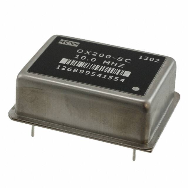


 工商网监
湘ICP备2023018690号
工商网监
湘ICP备2023018690号

