Available at Digi-Key**
www.digikey.com
Improved Performance
5x7mm
TB / TVB Model Series
TCXO / VCTCXO
2111 Comprehensive Drive
Aurora, Illinois 60505
Phone: 630- 851- 4722
Fax: 630- 851- 5040
www.conwin.com
Description:
Features:
Connor-Winfield's TBxxx
and TVBxxx series
TV
B5
0
10 4 12
are 5x7mm TCXO and
.0
MH 42
Z
VCTCXO products with
exceptional frequency
stability and low phase
noise.
Similar to our Txxx
/ TVxxx series, these devices are quieter,
smoother over temperature and are available at
higher frequencies.
Using the latest analog TCXO technology,
the TBxxx and TVBxxx series have improved
phase noise and frequency stability
performance and are available in 4-pad or 10pad surface mount footprints.
These products are designed for
such applications as IEEE 1588 PTP and
Synchronous Ethernet.
• Frequency Stabilities Available:
+/-0.28 ppm (10 to 50 MHz)
+/-0.50 ppm, +/-1.00 ppm or +/-2.00 ppm
(10 to 100 MHz)
• Temperature Ranges Available:
0 to 85°C, 0 to 70°C, -40 to 85°C or -20 to 70°C
• Packages Available:
TB - Series: 5 x 7mm - 10 Pad
TVB - Series: 5 x 7mm - 4 Pad
• 3.3 Vdc Operation
• Output Logic: LVCMOS or Clipped Sinewave
• Fixed Frequency - TCXO
• Voltage Controlled - VCTCXO
• Low Jitter 52 to 100 MHz)
-
-
12
mA
Clipped Sine (10 to 52 MHz)
-
1.3
2.9
mA
Clipped Sine (>52 to 100 MHz)
-
-
12
mA
Jitter:
Period Jitter
-
3.0
5.0
ps RMS
Integrated Phase Jitter (12K to Fo/2)
-
0.3
1.0
ps RMS
8
Allan Deviation (1s) Fo=10.0 MHz
-
1.0E-10
-
Typical SSB Phase Noise
For Fo
10.0 MHz
50.0 MHz
100.0 MHz
@ 10 Hz offset
-98
-70
-60
dBc/Hz
@ 100 Hz offset
-125
-100
-91
dBc/Hz
@ 1 KHz offset
-143
-122
-119
dBc/Hz
@ 10 KHz offset
-151
-145
-142
dBc/Hz
@ 100 KHz offset
-152
-150
-153
dBc/Hz
@ 1 MHz offset
-155
-152
-153
dBc/Hz
Start-Up Time
-
-
10
ms
Bulletin
Page
Revision
Date
Specifications subject to change without notification. See Connor-Winfield's website for latest revision.
© Copyright 2018 The Connor-Winfield Corporation Not intended for life support applications.
Tx380
2 of 6
10
07 Aug 2018
�2111 Comprehensive Drive
Aurora, Illinois 60505
Phone: 630- 851- 4722
Fax: 630- 851- 5040
www.conwin.com
Control Voltage Input Characteristics
ParameterMinimum
Minimum
Control Voltage
0.3
Frequency Pullability
Pull Range Options 4 and 5:
±10
Pull Range Option 9:
±5
Pull Slope (Vc=1.65V)
Pull Range Options 4 and 5:
-
Pull Range Option 9:
-
Control Voltage Slope
Monotonic Linearity
-
Input Impedance
100K
Modulation Bandwidth (3dB)
10
Nominal
1.65
Maximum
3.0
Units
V
±12
±6
-
±8
ppm
ppm
8.00
-
4.50
-
Positive Slope
-
5
-
-
-
-
Notes
ppm/V
ppm/V
%
Ohm
KHz
OE Enable /Disable Input Characteristics (Pad 8) TB Series only
Parameter
Enable Voltage (High)
Disable Voltage (Low)
Function
Low:
High or Open:
Minimum
70%Vcc
-
Nominal
-
-
Maximum
-
30%Vcc
Units
Vdc
Vdc
Notes
9
9
Maximum
Units
Notes
Units
Notes
Output
Disabled (High Impedance)
Enabled
LVCMOS Output Characteristics
Parameter
Load (CL)
Voltage (High) (Voh)
(Low)
(Vol)
Current (High) (Ioh)
(Low)
(Iol)
Duty Cycle at 50% of Vcc
Rise / Fall Time 10% to 90%
Minimum
-
90%Vcc
-
-4
-
45
-
Nominal
15
-
-
-
-
50
4
-
-
10%Vcc
-
4
55
8
pF
Vdc
Vdc
mA
mA
%
ns
10
Clipped Sinewave Output Characteristics
Parameter
Minimum
Nominal
Maximum
Load (RC)
Output Load Resistance
-
10K
-
Ohm
Output Load Capacitance
-
10
-
pF
Output Voltage(< 40 MHz)
1.0
1.2
-
V
Output Voltage(=>40 MHz)
0.8
1.0
-
V
Output Impedance
-
200
-
Ohms
11
12
pk-pk
pk-pk
Package Characteristics
Package
Hermetically sealed ceramic package with grounded metal cover
Environmental Characteristics
Vibration:
Shock:
Soldering Process:
Notes:
Vibration per Mil Std 883E Method 2007.3 Test Condition A.
Mechanical Shock per Mil Std 883E Method 2002.4 Test Condition B.
RoHS compliant lead free. See soldering profile on page 6.
1. Initial calibration @ 25°C. ±2°C, for VCTCXO's Vc = 1.65V. Specifications at time of shipment
2. Frequency stability vs. change in temperature. [±(Fmax-Fmin)/(2*Fo]). For VCTCXO, Vc = 1.65Vdc
3. Inclusive of frequency stability, supply voltage change (±1%), aging, for 24 hours. Per STRATUM 3 GR-1244-CORE.
4. Frequency change after reciprocal temperature ramped over the operating range. Frequency measured before and after at 25°C
5. Two consecutive solder reflows after 1 hour recovery @ 25°C.
6. Frequency drift over 1 year @ 25°C.
7. Inclusive of calibration @ 25°C, frequency vs. change in temperature, change in supply voltage (±5%), load change (±5%), reflow
soldering process and 20 years aging.
8. For Fo40MHz, BW=12kHz to 20MHz
9. Ouput is active with Pad 8 not connected. Leave Pad 8 open if disable function is not required. When disabled, output stage is off
but oscillator and compensation circuits are still powered (current consumption
很抱歉,暂时无法提供与“TB522-080.0M”相匹配的价格&库存,您可以联系我们找货
免费人工找货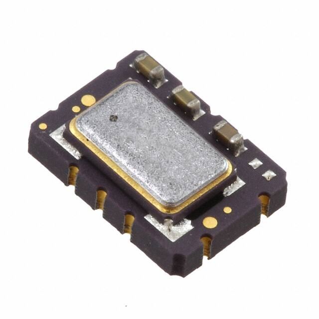


 工商网监
湘ICP备2023018690号
工商网监
湘ICP备2023018690号
