TCXO
Specification
Models TL602 and TVL602
2111 Comprehensive Drive
Aurora, Illinois 60505
Phone: 630- 851- 4722
Fax: 630- 851- 5040
Description:
Features:
The Connor-Winfield TL602 and TVL602
are surface mount 5x7mm, 3.3V, LVCMOS
Temperature Compensated Crystal
Oscillators (TCXO) designed for application
compliance to Telcordia Stratum 3, ITU-T
G.813 Option 2, and ITU-T G.8262 Option 2.
• 3.3 Vdc Operation
• Frequency Stability: ± 0.14 ppm
• Temperature Range: -40 to 85°C
• LVCMOS Output
• Ceramic Surface Mount Package
• Tape and Reel Packaging
• RoHS Compliant / Pb Free
Absolute Maximum Ratings
www.conwin.com
Parameter
US Headquarters:
630-851-4722
European Headquarters:
+353-61-472221
Storage Temperature
Supply Voltage (Vcc)
Input Voltage
Minimum
Nominal
Maximum
Units
-55
-0.5
-0.5
-
-
-
85
6.0
Vcc+0.5
°C
Vdc
Maximum
Units
Notes
Operating Specifications
Parameter
Nominal Frequency (Fo)
Frequency Calibration @ 25 °C
Frequency Stability vs. Temperature
Frequency vs. Load Stability
Frequency vs. Voltage Stability
Static Temperature Hysteresis
Short Term Allan Variance (1 second)
Constant Temperature Stability
Aging 1st Year
Total Tolerance
Operating Temperature Range:
Supply Voltage (Vcc)
Supply Current (Icc)
Period Jitter
Integrated Phase Jitter
SSB Phase Noise at 10Hz offset
SSB Phase Noise at 100Hz offset
SSB Phase Noise at 1KHz offset
SSB Phase Noise at 10KHz offset
SSB Phase Noise at 100KHz offset
Start-up Time
Minimum
Nominal
-
-1.0
-140
-50
-50
-
-
-40
-1.0
-4.6
-40
3.135
-
-
-
-
-
-
-
-
-
20.0 and 24.576M
-
-
-
-
-
1.0E-10
-
-
-
-
3.3
-
3
0.5
-80
-110
-135
-150
-150
-
-
1.0
140
50
50
0.40
-
40
1.0
4.6
85
3.465
6
5
1.0
-
-
-
-
-
1
Notes
MHz
ppm 1
ppb 2
ppb ±5%
ppb ±5%
ppm 3
ppb
24 Hours
ppm
ppm
°C
Vdc ±5%
mA
ps rms
ps rms 4
dBc/Hz
dBc/Hz
dBc/Hz
dBc/Hz
dBc/Hz
ms
Enable / Disable Input Characteristics (TL602 only)
Parameter
Minimum
Enable Voltage (High)
Disable Voltage (Low)
Nominal
Maximum
70%Vcc
-
-
-
30%Vcc
Units
Notes
Vdc
Vdc
5
5
LVCMOS Output Characteristics
Parameter
Load
Voltage (High) (Voh)
(Low)
(Vol)
Duty Cycle at 50% of Vcc
Rise / Fall Time 10% to 90%
Minimum
Nominal
Maximum
-
90%Vcc
-
45
-
15
-
-
50
4
-
-
10%Vcc
55
8
Units
Package Characteristics
Package
Hermetically sealed crystal mounted on a ceramic package
Environmental Characteristics
Vibration:
Shock:
Soldering Process;
Vibration per Mil Std 883E Method 2007.3 Test Condition A
Mechanical Shock per Mil Std 883E Method 2002.4 Test Condition B.
RoHS compliant lead free. See soldering profile on page 2.
Ordering Information
Bulletin
Page
Revision
Date
Tx414
1 of 3
02
19 March 2015
Notes
pF
Vdc
Vdc
%
ns
TL602-020.0M, TL602-024.576M, TVL602-020.0M, TVL602-024.576M
Notes:
1. Frequency referenced to Fo. @ 25°C. Specification at time of shipment after 48 hours operation
2. Frequency stability vs. change in temperature. [±(Fmax - Fmin)/2.Fo].
3. Frequency change after reciprocal temperature ramped over the operating range. Frequency measured before and after at 25°C.
4. Bandwidth = 12KHz to Fo/2 MHz.
5. Output is enabled with no connection on pad 8 (for TL602 only).
�2111 Comprehensive Drive
Aurora, Illinois 60505
Phone: 630- 851- 4722
Fax: 630- 851- 5040
www.conwin.com
TL602-020.0M Package Layout
TL602 Suggested Pad Layout
0.079 Max.
(2.0mm)
0.276 ±0.006
(7.0mm)
Pad
0.295
(7.49mm)
0.051
(1.28mm)
0.030
(0.76mm)
Keep Out Area
0.197
±0.006
(5.0mm)
TL602 1438
20.0 MHZ
8
0.037
(0.94mm)
0.215
(5.46mm)
0.025(6 Places)
(0.635mm)
Pin 1
10
0.030
(0.762mm)
(4 Places)
2
1
Temperature
3
220°C
120°C
0
10 s
Up to 120 s
60 to 90 s
Typical
Typical
Meets IPC/JEDEC J-STD-020C
0.100
(2.54mm)
Bottom
View
9
8
0.038
(0.965mm)
(4 Places)
7
0.040
(1.02mm)
(6 Places)
5
6
6
5
Top View
10
4
2
3
0.051
(1.28mm)
* Do not route any traces in the keep out area.
It is recommended the next layer under the
keep out area is to be ground plane.
Dimensional Tolerance:
±.005 (.127mm)
±.02 (.508mm)
0.100
(2.54mm)
7
9
1
4
260°C
260°C
180°C
150°C
TL602 Pad Connections
Connection
1: Do Not Connect
2: Do Not Connect
3: Do Not Connect
4: Ground
5: Output
6: Do Not Connect
7: Do Not Connect
8: Tri-State Enable / Disable
9: Supply Voltage Vcc
10: N/C
Output Waveform
Solder Profile
Temperature
TL602-024.576M Package Layout
260°C
260°C
220°C
TL602 1438
150°C
0.095
(2.4mm)
(2.4mm)
(7.0mm)
TL602 1438
24.576MHz
MHz
24.576
180°C
0.095
0.276 ±0.006
±0.006
(7.0mm)
0.276
120°C
0.197
0
0.197
±0.006
±0.006
(5.0mm)
(5.0mm)
10 s
Up to 120 s
60 to 90 s
Typical
Typical
1V/Div
Meets IPC/JEDEC J-STD-020C
TVL602-020.0M Package Layout
0.276 ±0.006
(7.0mm)
(Top View)
TVL602 Suggested Pad Layout
0.079 Max.
(2.0mm)
0.071
(1.8mm)
4 Places
4
TVL602 1511
20.0 MHZ
0.197
±0.006
(5.0mm)
0.165
(4.2mm)
0.034
(0.90mm)
(4 Places)
2
(Bottom View)
4
3
Dimensional Tolerance:
±.005 (.127mm)
±.02 (.508mm)
0.055
(1.40mm)
(4 Places)
0.047
(1.2mm)
4 Places
(Top View)
Pad 1
1
3
1
0.224
(5.7mm)
2
TVL602
Pad Connections
Pad
1:
2:
3:
4:
Connection
N/C
Ground
Output
Supply Voltage Vcc
Keep
Out *
Area
* Do not route any traces in the keep out area. It is
recommended the next layer under the keep out
area is to be ground plane.
TVL602-024.576M Package Layout
0.095
0.095
(2.4mm)
(2.4mm)
0.276 ±0.006
(7.0mm)
TL602 1438
TVL602
1511
24.576
MHz
24.576 MHz
0.197
0.197
±0.006
±0.006
(5.0mm)
(5.0mm)
Bulletin
Page
Revision
Date
Specifications subject to change without notification. See Connor-Winfield's website for latest revision. All dimensions in inches.
© Copyright 2015 The Connor-Winfield Corporation Not intended for life support applications.
Tx414
2 of 3
02
19 March 2015
�2111 Comprehensive Drive
Aurora, Illinois 60505
Phone: 630- 851- 4722
Fax: 630- 851- 5040
www.conwin.com
Design Recommendations
Vcc, should have
a large copper
area for reduced
inductance.
Connect a 0.01uF
bypass capacitor
很抱歉,暂时无法提供与“TL602-020.0M”相匹配的价格&库存,您可以联系我们找货
免费人工找货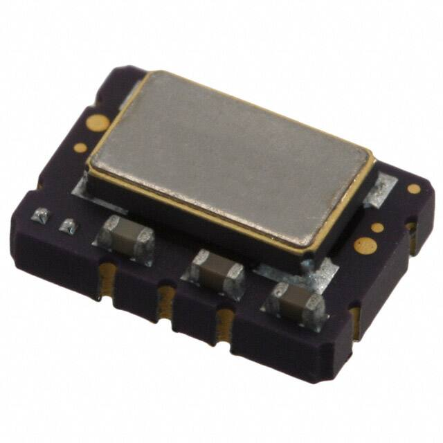


 工商网监
湘ICP备2023018690号
工商网监
湘ICP备2023018690号
