High Frequency
Low Jitter
VCXO
2111 Comprehensive Drive
Aurora, Illinois 60505
Phone: 630- 851- 4722
Fax: 630- 851- 5040
www.conwin.com
US Headquarters:
630-851-4722
European Headquarters:
+353-61-472221
Description
Features
The Connor-Winfield models V777,
V778, V787 and V788 are 3.3V, Surface
Mount 5.0x7.0mm, Voltage Controlled
Crystal Oscillator (VCXO) with LVPECL
differential outputs and enable/disable
function. The V777, V778, V787 and V788 are designed
for use with applications utilizing a PLL system requiring
very high frequency and low jitter. The surface mount
package is designed for high-density mounting and is
optimum for mass production.
• 3.3V Operation
• Absolute Pull Range (APR): ±30ppm
• Temperature Range: 0 to 70°C or
-40 to 85°C
• Differencial LVPECL Outputs
• Low Jitter 70fs RMS Typical
• Enable / Disable Function:
Models Vxx7: Enable Low
Models Vxx8: Enable High
• 5.0x7.0mm Surface Mount Package
• Tape and Reel Packaging
• RoHS Compliant / Lead Free
Absolute Maximum Ratings
Parameter
Storage Temperature
Supply Voltage (Vcc)
Input Voltage (Vc)
Minimum
-55
-0.5
-0.5
Nominal
-
-
-
Maximum
125
4.6
Vcc+0.5
Units
°C
Vdc
Vdc
Notes
Operating Specifications
Parameter
Minimum
Center Frequency: (Fo)
150
Operating Temperature Range:
Models Vx7x:
0
Models Vx8x:
-40
Supply Voltage: (Vcc)
3.135
Supply Current (lcc)
-
Integrated Phase Jitter (BW=12kHz to 20MHz) -
Typical Phase Noise for Fo = 245.76 MHz
SSB Phase Noise at 10Hz offset
-
SSB Phase Noise at 100Hz offset
-
SSB Phase Noise at 1KHz offset
-
SSB Phase Noise at 10KHz offset
-
SSB Phase Noise at 100KHz offset
-
SSB Phase Noise at 1MHz offset
-
SSB Phase Noise at 10MHz offset
-
Sub Harmonic Content
@ 25% Fo
-
@ 50% Fo
@ 75% Fo
Harmonic Content @ 2xFo
-
Spurious Content
-
Nominal
Maximum
Units
-
-
3.30
-
70
85
3.465
100
100
°C
°C
Vdc
mA
fs RMS
-60
-85
-110
-135
-150
-150
-158
-
-
-
-
-
-
-
dBc/Hz
dBc/Hz
dBc/Hz
dBc/Hz
dBc/Hz
dBc/Hz
dBc/Hz
-45
-40
-45
-17
-
-
-
-
-
-70
dBc
dBc
dBc
dBc
dBc
Maximum
Units
-
710
70
MHz
Notes
Input Characteristics
Parameter
Minimum
Control Voltage Range (Vc)
0.3
Tuning Slope (Kv)
-
Absolute Pull Range (APR)
±30
Monotonic Linearity
-10
Input Impedance
130K
Modulation Bandwidth (3dB)
25
Models: Vxx7 Enable / Disable Function
Enable Input Voltage (Low) (Vil)
-
Disable Input Voltage (High) (Vih) 2.275
Models: Vxx8 Enable / Disable Function
Enable Input Voltage (High) (Vil) 2.275
Disable Input Voltage (Low) (Vih) -
Nominal
1.65
80
-
-
180K
-
Notes
3.0
-
-
10
-
-
Vdc
ppm/V
ppm 1
%
Ohm
KHz
-
-
1.68
-
Vdc
Vdc 2
-
-
-
1.68
Vdc
Vdc 2
LVPECL Output Characteristics
Parameter
Bulletin
Page
Revision
Date
Vx605
1 of 2
05
13 April 2017
Load
Voltage (High) Voh
(Low) Vol
Duty Cycle at 50% Level
Rise / Fall Time 20% to 80%
Minimum
-
2.275
-
45
-
Nominal
-
-
-
50
0.30
Maximum
50
-
1.68
55
0.45
Units
Notes
Ohms 3
Vdc
Vdc
%
ns
�2111
2111
Comprehensive
Comprehensive
Drive
Drive
Aurora,
Aurora,
Illinois
Illinois
60505
60505
2111 Comprehensive
Drive
2111 Comprehensive Drive
Aurora, Phone:
Illinois
60505
Phone:
630-851-4722
630-851-4722
Aurora,
Illinois 60505
Phone: 630-851-4722
Fax:
Fax:
630-851-5040
630-851-5040
Phone:
630- 851- 4722
Fax: 630-851-5040
www.conwin.com
www.conwin.com
Fax: 630- 851- 5040
www.conwin.com
www.conwin.com
Models
Models
: V777-V787
: V777-V787
EModels
nable
E nable
Dis
/ Dis
able
able
F unc
F unc
tion
tion
(P(P
adad
2)/2)Disable
Output
Output
Enable
Function
:/V777-V787
S oldering Proces s
R oHS compliant, lead free. S ee s older profile.
NoNo
C
onnection
C onnection
E nable
E nable
/ Dis able
F unc
tion
(P ad Vxx7
2)
Output E nable
Models:
Package Hermetically sealed ceramic package with grounded metal
cover.
Low
Low/ Disable Function (Pad
E nable Output
Enable
2) E nable
No C onnection
E nable
Soldering Process RoHS compliant, lead free. See Solder Profile.
HighNo Connection Disable
Disable
(High
Impedance)
Impedance)
Low High
E nable(High
Enable
Notes
High
LowDisable (High Impedance) Enable
Models
Models
: V778-V788
: V778-V788
1 Absolute pull range (APR) is the minimum guaranteed pull range of the VCXO
Disable (High Impedance)
High
:/ V778-V788
nable
E nable
Dis
/ Dis
able
able
F unc
F unc
tion
tion
(P(P
adad
2) 2)
Output
Output
under all conditions over the lifetime operation. Including calibration @ 25°C, EModels
E nable / Dis able
F
unc
tion
(P
ad
2)
Output
Models:
Vxx8
frequency vs change in temperature, frequency vs. change in supply voltage,
NoNo
C onnection
C onnection
E nable
E nable
frequency vs. change in load, shock and vibration and aging for ten years.
Enable
2) E nable
No C onnection
E nable
High
High/ Disable Function (Pad
E nable Output
The APR is referenced to Fo. Positive Transfer Function.
High Low
E nable(High
Enable
LowNo Connection Disable
Disable
(High
Impedance)
Impedance)
2. Outputs are enabled with no connection on pad 2. When oscillator is disabled
Low
HighDisable (High Impedance) Enable
both outputs are in high impedance state.
Disable (High Impedance)
Low
3. 50 ohm termination into Vcc-2V or Thevein equivalent.
R oHS
R oHS
compliant,
compliant,
lead
lead
free.
free.
S ee
S ee
s older
s older
profile.
profile.
Packaging
Characteristics
S oldering
S oldering
Proces
Proces
s s
Package Layout
0.275
0.275
0.2750.275
(7.0mm)
(7.0mm)
6 (7.0mm)
6 (7.0mm)
5
4 4
6 6 5 5 5
4
4
CW
CW 1412
1412
1412
CW
1715
V778
V778
V778
V778
(5.0mm)
622.08
622.08
622.08
M MM
Bottom
Bottom
Bottom
Bottom
View
ViewView
0.197
0.197
0.197
0.197
(5.0mm)
(5.0mm)
(5.0mm)
622.08M
1 1 1 2 2 2 3 3 3
1
0.070
0.070
0.070
(1.8mm)
(1.8mm)
(1.8mm)
0.070
2
3
(1.8mm)
View
Suggested Pad Layout
View
(4.2mm)
(4.2mm) View
1
1 1
2
2 2
3
3
1.65V
1.65V
1.65V
Pad Connections
P adPPad
P adConnection
tion tion
ad
P ad
PCad
Ponnec
ad
C onnec
C onnec
tion
Voltage
1 11: Control
Voltage
1 C ontrol
C ontrol
C ontrol
Voltage
Voltage Q
Disable 80%
2 2: Enable
E nable / Dis/able
22
E nable
E nable
/ Dis
/ Dis
able
able 50%
(Case)
3 3: Ground
G round (C as
e)
33
G round
G round
(C(C
asas
e)e) 20%
Bypass
4 4: Output
Output QQ
Q
Bypass
Bypass
Capacitor
44
Output
Output
QQ
Capacitor
Capacitor 5 5: Output
0.01uF
Output QQ
0.01uF
0.01uF
5
5
Output
Output
Q
Q
3Ground
6 6: Vcc
Vcc
Ground
Ground
0.070
66
Vcc
Vcc
Rt =
45 / 55
45 /45
55/ 55
45 / 55
Temperature
Temperature
Duty
Duty
Cycle
Cycle
260°C
45 /45
55/ 55
Q Q
Solder Profile
260°C
260°C
Temperature
Temperature
220°C
260°C
260°C
260°C
260°C
260°C
180°C
220°C
220°C
220°C
150°C
180°C
180°C
180°C
150°C
120°C
150°C
150°C
120°C
80%
80%
50%
50%
Rt Rt
Rt =
Rt =
Output Waveform
Duty Cycle
Rt Rt Rt
Rt
E/DE/D
E/D
Vcc = Vcc2
==3.3Vdc
VccVcc
Vcc2
= Vcc2
= 3.3Vdc
= 3.3Vdc
+/-0.008 (+/-0.2mm)
(5.08mm)
(5.08mm)0.100
0.100
0.100
(2.54mm)
(2.54mm)
(2.54mm)
4
6
5
0.079
4(2.0mm)
4 0.079
6 6
5 5
0.079
(2.0mm)
(2.0mm)
Top
0.165
TopTop
0.165
0.165 View
(4.2mm)
2 2
2
1 1
1
0.102
0.102
0.102
1
(2.6mm)
(2.6mm)
(2.6mm)
Dimensional
Dimensional
Dimensional
0.102
Tolerance
+/-0.008
(+/-0.2mm)
Tolerance
Tolerance
+/-0.008
+/-0.008
(+/-0.2mm)
(+/-0.2mm)
(2.6mm) Dimensional
Tolerance
0.200
0.200
0.200
(5.08mm)
Test Circuit
0.055
0.055
0.055
0.055
(1.4mm)
(1.4mm)
(1.4mm) (1.4mm)
120°C
120°C
20%
20%
Q Q
tr
tr tr
0
0
tf
0
tf tf
0
120 S
Max.
(1.78mm)
0.070
0.070
(1.78mm)
(1.78mm)
Time
10 S
10 s
s
60 S120Up
120
S toS 120
10 S10
60Sto 90 s
Max.Max.Max.
Typical
60 S60 Typical
S
360 Sec. Max.
Max.Max.
TimeTime
360 360
Sec.Sec.
Max.Max.
Meets IPC/JEDEC J-STD-020C
Tape and Reel
V7
7
Phase Noise Plot
622.08M
8
622.08M
77
V Temperature
V7 7
- 622.08M
8 8Output-Frequency:
R ange: E nable/Dias ble:
Frequency Format
7 = 0 to 70° C
7= E nable Low
Output
Output
Frequency:
Frequency:
R ange:
R ange:E nable/Diasble:
EHigh
nable/Diasble:
-xxx.xM Min.*
8 = -40Temperature
to Temperature
85 ° C
8 = E nable
Frequency
Frequency
Format
Format
7 =7 0=to0 70°
to 70°
C C
1
-xxx.xxxxxxM
Max.*
7= 7=
E nable
E nable
LowLow
-xxx.xM
-xxx.xM
Min.*
Min.*
*Amount
of numbers
8 =8 -40
= -40
toS 85
to °85
C °Voltage:
C
8 =8 E=nable
E nable
High
High
APR :
upply
-xxx.xxxxxxM
Max.*
Max.*
after the decimal-xxx.xxxxxxM
point.
+ /-30ppm
3.3Vdc
*Amount
of numbers
of numbers
M = MHz*Amount
1
APRAPR
: :
S upply
S upply
Voltage:
Voltage:
afterafter
the the
decimal
decimal
point.
point.
+ /-30ppm
+ /-30ppm
3.3Vdc
3.3Vdc
M =MMHz
= MHz
E xample:
V778-622.08M = 5x7mm, LVPE C L, VC XO,
E xample:
3.3Vdc, -40 to 85C , E+xample:
/-30APR
,
US Headquarters:
V778-622.08M
V778-622.08M
5x7mm,
= 5x7mm,
LVPE
LVPE
C L,CVC
L, VC
XO,XO,
Output
Frequency =622.08MHz
1
3.3Vdc,
3.3Vdc,
-40-40
to 85C
to 85C
, + ,/-30APR
+ /-30APR
, 630-851-4722
,
USUS
Headquarters:
Headquarters:
European Headquarters:
Output
Output
Frequency
Frequency
622.08MHz
622.08MHz
630-851-4722
630-851-4722
European
European
Headquarters:
Headquarters:
+ 353-61-472221
+ 353-61-472221
+ 353-61-472221
Bulle tin
Vx605
Page
Bulle
Bulle
tintin 2 of 2
Re vision Page
03
Page
Specifications subject to change without notice. All dimensions in inches. © Copyright 2008 The Connor-Winfield Corporation
Ordering Information
Specifications
Specifications
subject
subject
to change
to change
without
without
notice.
notice.
All All
dimensions
dimensions
in inches.
in inches.
© Copyright
© Copyright
2008
2008
TheThe
Connor-Winfield
Connor-Winfield
Corporation
Corporation
V7
Type
V7 = LVPECL
5 x 7mm
VCXO Series
7
Temperature
Range
7 = 0 to 70°C
8 = -40 to 85°C
APR: ±30ppm
8
622.08M
Enable/Disable
Output Frequency:
7 = Enable Low
8 = Enable High
Frequency Format
-xxx.xM Min*
-xxx.xxxxxxM Max*
*Amount of numbers after the
decimal point. M = MHz
Supply Voltage
3.3Vdc
Example:
V778-622.08M = 5x7mm, LVPECL, VCXO
3.3Vdc, 0 to 70°C, ±30APR,
Output Frequency 622.08MHz
Specifications subject to change without notification. See Connor-Winfield's website for latest revision.
© Copyright 2017 The Connor-Winfield Corporation Not intended for life support applications.
Da te
15 Se p 2011
ReRe
vision
vision
DaDa
te te
0303
1515
SeSe
p 2011
p 2011
Bulletin
Page
Revision
Date
Vx605
Vx605
2 of
2 of
2 2
Vx605
2 of 2
05
13 April 2017
�
很抱歉,暂时无法提供与“V788-622.08M”相匹配的价格&库存,您可以联系我们找货
免费人工找货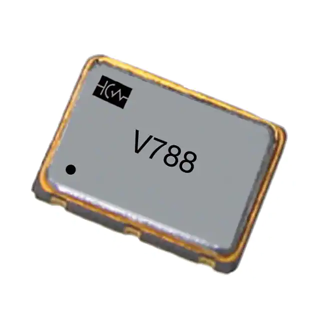


 工商网监
湘ICP备2023018690号
工商网监
湘ICP备2023018690号
