CPLL66-3160-3380
0.60" SQ SMD
Features
1GHz-5GHz Range Standard 3 Wire Interface Small layout 0.6" x 0.6"
Applications
Digital Radio Equipment Fixed Wireless Access Satellite Communications Systems Base Stations Personal Communications Systems Portable Radios Test Instruments Wireless Infrastructure
The CPLL66 is a complete PLL/Synthesizer needing only an external frequency reference and supply voltages for the internal PLL (phase lock loop) and VCO (voltage controlled oscillator). The Crystek CPLL66 is programmed using a standard three line interface (Data, Clock and Load Enable). The newly introduced CPLL66 family has been initially released to cover 1GHz to 5GHz in bands. It is housed in a compact 0.6-in. x 0.6-in. x 0.15-in. SMD package which saves board space. Typical phase noise at 4GHz is -90dBc/Hz at 10KHz offset with 0dBm minimum output power.
Rev. C
Page 1 of 6
�CPLL66-3160-3380
0.60" SQ SMD
UNITS GHz KHz msec dBm dBc/Hz dBc/Hz dBc/Hz dBc/Hz Volts Volts mA mA -60 -70 -10 -15 5 dBc dBc dBc dBc MHz dBm Ohm Ohm °C P ERFORMANCE SPECIFICATION Frequency Range: Step Size Settling Time Output Pow er: Output Phase Noise @1KHz offset @10KHz offset @100KHz offset @1MHz offset Pow er Supply V1=VCO Supply V2=PLL Supply Supply Current I1=VCO Input Current I2=PLL Input Current Spurious Suppression PFDSpur Reference Feedthru Harmonic Suppression (2nd Harmonic): 2nd 3rd Reference Frequency RF Output Level Input Impedance Rf Output Impedance Operating Temperature Range: MIN 3.160 TYP 2500 3 3 -85 -95 -115 -135 4.75 2.7 5 3 50 25 -70 -80 -15 -25 10 0 100K 50 MAX 3.380
0
6 -80 -90 -110 -130 5.25 3.3
-5
-40
+85
Output Phase Noise:
Page 2 of 6
�CPLL66-3160-3380
0.60" SQ SMD
TOP VIEW
0.600 0.500 0.420 0.340 0.260 0.180 0.100
BOTTOM VIEW
0.00 GND GND GND GND GND GND 0.00
CRYSTEK
CPLL66 2400-2500 Date Code
0.140 0.220 0.300 0.380 0.460 0.600
GND REF V2 V1 RF GND GND GND GND GND GND
LE DATA CLK LD N/C
TOP ORIENTATION MARK
LE= Load Enable, CMOS Input DATA= Serial Data Input CLK= Serial Data Input LD= Lock Detect REF= Reference Input V1= Analog Supply Input (VCO) V2= Digital Supply Input (PLL) RF= RF Output
BOTTOM ORIENTATION MARK
0.042 0.000 0.000 0.030 0.060 0.220
RECOMMENDED REFLOW SOLDERING PROFILE
Ramp-Up 3°C/Sec Max. Critical Temperature Zone Ramp-Down 6°C/Sec.
260°C TEMPERATURE 217°C 200°C 150°C
Preheat 180 Secs. Max. 8 Minutes Max.
0.000
Pad Detail
90 Secs. Max.
260°C for 10 Secs. Max.
Page 3 of 6
�CPLL66-3160-3380
0.60" SQ SMD
ENVIRONMENTAL COMPLIANCE Parameter Mechanical Shock Mechanical Vibration Solderability Resistance to Solvents Conditions MIL-STD-883, Method 2002 MIL-STD-883, Method 2007 MIL-STD-883, Method 1014 MIL-STD-883, Method 2016
Programming Guide for CPLL66-XXXX
Introduction
The CPLL66 uses a simple 3 wire interface to program four internal registers. See Figure 1.
Figure 1. Timing Diagram There are four 24 bit registers that need to be programmed. Which register is written into is simply controlled by Control Bits C1 and C2. Table I summarizes the Truth Table for Control Bits C1 and C2.
Table I. C2, C1 Truth Table Control Bits C2 C1 0 0 0 1 1 0 1 1 Data Latch R Counter N Counter (A and B) Function Latch (Including Prescaler) Initialization Latch
Table II shows the details of the four 24 bit registers.
Page 4 of 6
�CPLL66-3160-3380
0.60" SQ SMD
Table II. Latch Summary
REFERENCE COUNTER LATCH
LOCK DETECT PRECISION TEST MODE BITS ANTIBACKLASH WIDTH DB17 ABP2 DB16 ABP1 DB15 R14 DB14 R13 DB13 R12 DB12 R11 DB11 R10 CONTROL BITS
RESERVED
14-BIT REFERENCE COUNTER
DB23 X
DB22 0
DB21 0
DB20 LDP
DB19 T2
DB18 T1
DB10 R9
DB9 R8
DB8 R7
DB7 R6
DB6 R5
DB5 R4
DB4 R3
DB3 R2
DB2 R1
DB1 C2 (0)
DB0 C1 (0)
N COUNTER LATCH
CP GAIN CONTROL BITS
RESERVED
13-BIT B COUNTER
6-BIT A COUNTER
DB23
DB22
DB21 G1
DB20 B13
DB19 B12
DB18 B11
DB17 B10
DB16 B9
DB15 B8
DB14 B7
DB13 B6
DB12 B5
DB11 B4
DB10 B3
DB9 B2
DB8 B1
DB7 A6
DB6 A5
DB5 A4
DB4 A3
DB3 A2
DB2 A1
DB1 C2 (0)
DB0 C1 (1)
FUNCTION LATCH
FASTLOCK MODE FASTLOCK ENABLE CP THREESTATE PD POLARITY PRESCALER VALUE CURRENT SETTING 2 DB20 CP16 DB19 CP15 DB18 CP14 DB17 CP13 CURRENT SETTING 1 DB16 CP12 DB15 CP11 DB14 TC4 TIMER COUNTER CONTROL MUXOUT CONTROL COUNTER RESET DB2 F1 POWERDOWN 2 POWERDOWN 1 CONTROL BITS
DB23 P2
DB22 P1
DB21 PD2
DB13 TC3
DB12 TC2
DB11 TC1
DB10 F5
DB9 F4
DB8 F3
DB7 F2
DB6 M3
DB5 M2
DB4 M1
DB3 PD1
DB1 C2 (1)
DB0 C1 (0)
INITIALIZATION LATCH
FASTLOCK MODE FASTLOCK ENABLE CP THREESTATE PD POLARITY PRESCALER VALUE CURRENT SETTING 2 DB20 CP16 DB19 CP15 DB18 CP14 DB17 CP13 CURRENT SETTING 1 DB16 CP12 DB15 CP11 DB14 TC4 TIMER COUNTER CONTROL MUXOUT CONTROL COUNTER RESET DB2 F1 POWERDOWN 2 POWERDOWN 1 CONTROL BITS
DB23 P2
DB22 P1
DB21 PD2
DB13 TC3
DB12 TC2
DB11 TC1
DB10 F5
DB9 F4
DB8 F3
DB7 F2
DB6 M3
DB5 M2
DB4 M1
DB3 PD1
DB1 C2 (1)
DB0 C1 (1)
When using the CPLL66 family in a synthesizer application, all four 24 bit registers need to be written into after power-up. After writing all four latches the first time, subsequent frequency step changes can be accomplished by changing the N Counter Latch only.
Page 5 of 6
�CPLL66-3160-3380
0.60" SQ SMD
Programming Crystek p/n: CPLL66-3160-3380
The following is specific programming for CPLL66-3160-3380 (3.160GHz~3.380GHz with 2500KHz Step Size and 10MHz input reference frequency). Program all three registers with the following: Function Latch: 9F8083 H N Counter Latch: 002741 H R Counter Latch: 000013 H The above values will set the CPLL66-3160-3380 to 3.160GHz
Page 6 of 6
�
很抱歉,暂时无法提供与“CPLL66-3160-3380”相匹配的价格&库存,您可以联系我们找货
免费人工找货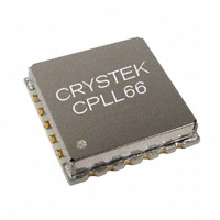


 工商网监
湘ICP备2023018690号
工商网监
湘ICP备2023018690号
