Additional Resources:
Product Page
date
09/04/2012
page
1 of 5
SERIES: VBSD1-SIP │ DESCRIPTION: DC-DC CONVERTER
1 W isolated output
industry standard 4 pin SIP package
single unregulated outputs
1,000 V isolation
UL safety approvals
wide temperature (-40~85°C)
efficiency up to 81%
U
•
•
•
•
•
•
•
ED
FEATURES
input
voltage
MODEL
output
voltage
range
(Vdc)
(Vdc)
VBSD1-S3.3-S3.3-SIP
3.3
3.0~3.6
VBSD1-S3.3-S5-SIP
3.3
VBSD1-S5-S3.3-SIP
5
VBSD1-S5-S5-SIP
VBSD1-S5-S9-SIP
output
current
output
power
ripple1
noise1
efficiency
min
(mA)
max
(mA)
max
(W)
max
(mVp-p)
max
(mVp-p)
typ
(%)
3.3
30
300
1
75
150
72
3.0~3.6
5
20
200
1
75
150
73
4.5~5.5
3.3
30
300
1
75
150
74
5
4.5~5.5
5
20
200
1
75
150
78
5
4.5~5.5
9
12
111
1
75
150
79
VBSD1-S5-S12-SIP
5
4.5~5.5
12
9
83
1
75
150
80
VBSD1-S5-S15-SIP
5
4.5~5.5
15
7
67
1
75
150
78
N
TI
typ
(Vdc)
N
RoHS
12
10.8~13.2
3.3
30
300
1
75
150
75
12
10.8~13.2
5
20
200
1
75
150
78
12
10.8~13.2
9
12
111
1
75
150
80
12
10.8~13.2
12
9
83
1
75
150
81
12
10.8~13.2
15
7
67
1
75
150
79
15
13.5~16.5
3.3
30
300
1
75
150
73
VBSD1-S15-S5-SIP
15
13.5~16.5
5
20
200
1
75
150
74
VBSD1-S15-S9-SIP
15
13.5~16.5
9
12
111
1
75
150
75
VBSD1-S15-S12-SIP
15
13.5~16.5
12
9
83
1
75
150
79
VBSD1-S15-S15-SIP
15
13.5~16.5
15
7
67
1
75
150
79
VBSD1-S24-S3.3-SIP
24
21.6~26.4
3.3
30
300
1
75
150
76
VBSD1-S24-S5-SIP
24
21.6~26.4
5
20
200
1
75
150
79
VBSD1-S24-S9-SIP
24
21.6~26.4
9
12
111
1
75
150
80
VBSD1-S24-S12-SIP
24
21.6~26.4
12
9
83
1
75
150
81
VBSD1-S24-S15-SIP
24
21.6~26.4
15
7
67
1
75
150
79
VBSD1-S24-S24-SIP
24
21.6~26.4
24
4
42
1
75
150
80
VBSD1-S12-S9-SIP
VBSD1-S12-S12-SIP
VBSD1-S12-S15-SIP
D
IS
C
VBSD1-S15-S3.3-SIP
O
VBSD1-S12-S3.3-SIP
VBSD1-S12-S5-SIP
Notes:
1. ripple and noise are measured at 20 MHz BW
cui.com
�Additional Resources:
Product Page
CUI Inc │ SERIES: VBSD1-SIP │ DESCRIPTION: DC-DC CONVERTER
date 09/04/2012 │ page 2 of 5
PART NUMBER KEY
Base Number
Input Voltage
Output Voltage
ED
VBSD1 - SXX - SXX -SIP
Packaging Style
INPUT
conditions/description
min
operating input voltage
3.3 V model
5 V model
12 V model
15 V model
24 V model
2.97
4.5
10.8
13.5
21.6
N
OUTPUT
conditions/description
line regulation
for Vin change of 1%, 3.3 V model
for Vin change of 1%, all other models
min
load regulation
measured from 10% load to full load
3.3 V model
5 V model
9 V model
12 V model
15 V model
TI
parameter
see derating curves
switching frequency
100% load, input voltage range
N
voltage accuracy
PROTECTIONS
parameter
conditions/description
min
IS
C
short circuit protection
O
temperature coefficient
typ
max
units
3
5
12
15
24
3.63
5.5
13.2
16.5
26.4
Vdc
Vdc
Vdc
Vdc
Vdc
typ
max
units
1.5
1.2
%
%
20
15
15
15
15
%
%
%
%
%
U
parameter
15
12.8
8.3
6.8
6.3
100
kHz
±0.03
%/°C
typ
max
units
1
s
max
units
SAFETY AND COMPLIANCE
parameter
conditions/description
min
isolation voltage
for 1 minute at 1 mA max.
1,000
Vdc
isolation resistance
at 500 Vdc
1,000
MΩ
safety approvals
UL 60950-1 (E222736)
3,500,000
hours
MTBF
burn-in
full load at 85°C, 4 hours at no load and 4 hours at full load
RoHS compliant
yes
typ
D
ENVIRONMENTAL
parameter
conditions/description
min
operating temperature
storage temperature
storage humidity
non-condensing
temperature rise
at full load
lead temperature
1.5 mm from case for 10 seconds
max
units
-40
typ
85
°C
-55
125
°C
95
%
25
°C
300
°C
15
cui.com
�Additional Resources:
Product Page
CUI Inc │ SERIES: VBSD1-SIP │ DESCRIPTION: DC-DC CONVERTER
date 09/04/2012 │ page 3 of 5
DERATING CURVES
2. output voltage vs. output current
ED
1. output power vs. ambient temperature
+10%
80
60
40
-20
0
20
40
60
85
100
Voltage
120
N
0.46 x 0.23 x 0.39 (11.70 x 6.00 x 10.00 mm)
min
case material
plastic (UL94-V0)
N
TI
conditions/description
dimensions
+0.15
0
(0.1)
(0.1)
2.54
O
Side View
12 3
4
PIN CONNECTIONS
Bottom View
PIN
1 2 3 4
D
IS
C
100%
Output Current (%)
parameter
units: mm [inches]
tolerance: ±0.25 [±0.010]
pin section tolerance: ±0.10 mm [±0.004]
50%
10%
MECHANICAL
MECHANICAL DRAWING
-2.5%
-7.5%
Ambient Temperature (°C)
weight
+2.5%
Nominal
U
20
-40
+5%
Output Voltate (%)
Load (%)
100
cui.com
FUNCTION
1
GND
2
+Vin
3
0V
4
+Vo
typ
max
units
inch
2.1
g
�Additional Resources:
Product Page
CUI Inc │ SERIES: VBSD1-SIP │ DESCRIPTION: DC-DC CONVERTER
date 09/04/2012 │ page 4 of 5
APPLICATION NOTES
Requirement on Output Load
In order to ensure the product operates efficiently and reliably, make sure the specified range of input voltage is not exceeded and the
minimum output load is not less than 10% load. If the actual load is less than the specified minimum load, the output ripple may
increase sharply while its efficiency and reliability will reduce greatly. If the actual output power is very small, please add an
appropriate resistor as extra loading.
2.
Overload Protection
Under normal operating conditions, the output circuit of these products has no protection against over-current and short-circuits. The
simplest method is to connect a self-recovery fuse in series at the input end or add a circuit breaker to the circuit.
3.
Filtering
In some circuits which are sensitive to noise and ripple, a filtering capacitor may be added to the DC/DC output end and input end to
reduce the noise and ripple. However, the capacitance of the output filter capacitor must be proper. If the capacitance is too big, a
startup problem might arise. For every channel of output, provided the safe and reliable operation is ensured, the greatest
capacitance of its filter capacitor sees the external capacitor table. To get an extremely low ripple, an “LC” filtering network may be
connected to the input and output ends of the DC/DC converter, which may produce a more significant filtering effect. It should also
be noted that the inductance and the frequency of the “LC” filtering network should be staggered with the DC/DC frequency to avoid
mutual interference (Figure 1).
Figure 1
+Vout
DC DC
&
-Vin
&
-Vout
TI
4.
L
N
L
+Vin
U
ED
1.
Output Voltage Regulation and Over-voltage Protection Circuit
The simplest device for output voltage regulation, over-voltage and over-current protection is a linear voltage regulator with overheat
protection that is connected to the input or output end in series (Figure 2).
+Vin
+Vout
REG
DC DC
N
Figure 2
-Vin
+Vin
-Vout
+Vout
REG
O
DC DC
-Vin
External Capacitor Table
It is not recommended to connect any external capacitor in the application field with less than 0.5 W output.
IS
C
5.
-Vout
Cout
(μF)
Vout
(Vdc)
Cout
(μF)
3.3/5
4.7
3.3
10
12
2.2
5
10
24
1
9
4.7
--
--
12
2.2
--
--
15
1
D
Table 1
Vin
(Vdc)
cui.com
�Additional Resources:
Product Page
CUI Inc │ SERIES: VBSD1-SIP │ DESCRIPTION: DC-DC CONVERTER
date 09/04/2012 │ page 5 of 5
REVISION HISTORY
description
date
09/01/2009
1.0
initial release
1.01
new template applied
1.02
V-Infinity branding removed
ED
rev.
04/10/2012
09/04/2012
D
IS
C
O
N
TI
N
U
The revision history provided is for informational purposes only and is believed to be accurate.
Headquarters
20050 SW 112th Ave.
Tualatin, OR 97062
800.275.4899
Fax 503.612.2383
cui.com
techsupport@cui.com
CUI offers a two (2) year limited warranty. Complete warranty information is listed on our website.
CUI reserves the right to make changes to the product at any time without notice. Information provided by CUI is believed to be accurate and reliable. However, no responsibility is
assumed by CUI for its use, nor for any infringements of patents or other rights of third parties which may result from its use.
CUI products are not authorized or warranted for use as critical components in equipment that requires an extremely high level of reliability. A critical
component is any component of a life support device or system whose failure to perform can be reasonably expected to cause the failure of the life support device or system, or to
affect its safety or effectiveness.
�
很抱歉,暂时无法提供与“VBSD1-S12-S12-SIP”相匹配的价格&库存,您可以联系我们找货
免费人工找货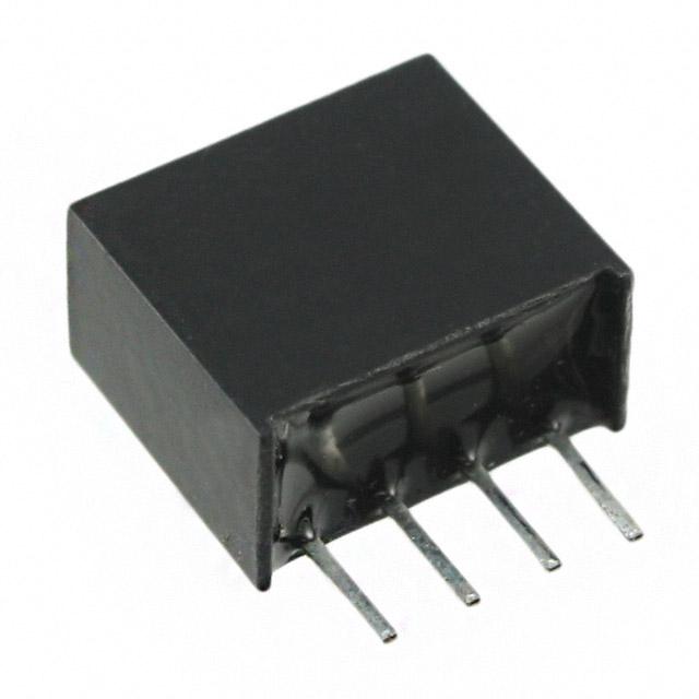


 工商网监
湘ICP备2023018690号
工商网监
湘ICP备2023018690号
