Please note that Cypress is an Infineon Technologies Company.
The document following this cover page is marked as “Cypress” document as this is the
company that originally developed the product. Please note that Infineon will continue
to offer the product to new and existing customers as part of the Infineon product
portfolio.
Continuity of document content
The fact that Infineon offers the following product as part of the Infineon product
portfolio does not lead to any changes to this document. Future revisions will occur
when appropriate, and any changes will be set out on the document history page.
Continuity of ordering part numbers
Infineon continues to support existing part numbers. Please continue to use the
ordering part numbers listed in the datasheet for ordering.
www.infineon.com
�CY27410
4-PLL Spread-Spectrum Clock Generator
4-PLL Spread-Spectrum Clock Generator
Features
■
Input frequencies
❐ Crystal input: 8 MHz to 48 MHz
❐ Reference clock: 8 MHz to 250 MHz LVCMOS
❐ Reference clock: 8 MHz to 700 MHz differential
■
Output frequencies
❐ 25 MHz to 700 MHz LVDS, LVPECL, HCSL, CML
❐ 3 MHz to 250 MHz LVCMOS
❐ 1 kHz to 8 MHz for one LVCMOS output
■
Up to 100-ps skew for differential outputs within a bank
■
Four fractional N-type phase-locked loops (PLLs) with
❐ VCXO (±120 ppm with steps of 0.23 ppm)
❐ Spread-spectrum capability (Logic SS and Lexmark profile
0.1% to 5% in 0.1% steps, down or center spread)
■
Supply voltage: 1.8 V, 2.5 V, and 3.3 V
■
Zero-delay buffer (ZDB) and non-zero delay buffer (NZDB)
configurations
■
I2C configurable with onboard programming
■
RMS phase jitter: 1-ps max at 12-kHz to 20-MHz offset
■
PCIe 1.0/2.0/3.0 compliant
■
SATA 2.0, USB 2.0/3.0, 1/10-GbE compliant
Functional Description
■
Maximum 12 outputs split in two banks with six outputs each.
❐ Up to eight differential output pairs (HCSL, LVPECL, CML,
or LVDS)
❐ Up to 12 LVCMOS outputs
The CY27410 device configuration can be created using
ClockWizard 2.1. For programming support, contact Cypress
technical support or send an email to clocks@cypress.com.
■
Industrial-grade device, offered in 48-pin QFN (7 × 7 × 1.0 mm)
package
For a complete list of related documentation, click here.
OUT16
OUT15
VDDIO_S1
VDDIO_D1
OUT14P
OUT14N
OUT13P
OUT13N
OUT12P
OUT12N
OUT11P
OUT11N
Logic Block Diagram
O1[1..4]
O2[1..4]
FS
PLL1
PLL2
I2C
INC
IN1S
IN2S
XIN
INC
IN1S
IN2S
O2[1..4]
ADC
OUTC
O1[1..4]
Output Drivers 1
VIN
FS2
FS1
FS0
SCLK
SDAT
RCAL
XOUT
INI
IN1S
IN2S
INC
RCCAL
Register
Memory
BG
INC
IN1S
IN2S
IN2N
INC
IN1S
IN2S
IN2P
Reference
System
OUTC
IN1P
IN1N
PLL3
OSC
PLL4
O3[1..4]
O4[1..4]
O3[1..4]
O4[1..4]
NV
Memory
POR
QP
PRG
Block
LDOs
VDD
Cypress Semiconductor Corporation
Document Number: 001-89074 Rev. *M
•
198 Champion Court
OUT26
OUT25
VDDIO_S2
VDDIO_D2
OUT24P
OUT24N
OUT23P
OUT23N
OUT22P
OUT22N
OUT21P
OUT21N
Output Drivers 2
•
San Jose, CA 95134-1709
•
408-943-2600
Revised February 15, 2019
�CY27410
Contents
Functional Overview ........................................................ 3
Input System ............................................................... 3
VCXO Input Block ....................................................... 3
Frequency Select Input ............................................... 3
I2C Block (SCLK, SDAT) ............................................. 4
Synthesis Section ........................................................ 4
Output Section ............................................................. 4
Onboard Programming ................................................ 5
Functional Features
and Application Considerations .......................................... 5
Pinouts ............................................................................ 10
Electrical Specifications ................................................ 13
Absolute Maximum Ratings ....................................... 13
Operating Temperature ............................................. 13
Operating Power Supply ........................................... 13
DC Chip-Level Specifications .................................... 14
DC Output Specifications .......................................... 15
AC Input Clock Specifications ................................... 16
Document Number: 001-89074 Rev. *M
AC Output Specifications .......................................... 16
Test and Measurement Circuits ................................ 23
Voltage and Timing Definitions .................................. 24
Packaging Information ................................................... 26
Solder Reflow Specifications ..................................... 26
Ordering Information ...................................................... 27
Ordering Code Definitions ......................................... 27
Acronyms ........................................................................ 28
Document Conventions ................................................. 28
Units of Measure ....................................................... 28
Document History Page ................................................. 29
Sales, Solutions, and Legal Information ...................... 30
Worldwide Sales and Design Support ....................... 30
Products .................................................................... 30
PSoC® Solutions ...................................................... 30
Cypress Developer Community ................................. 30
Technical Support ..................................................... 30
Page 2 of 30
�CY27410
Functional Overview
The CY27410 is a standard-performance programmable clock
generator with four independent fractional PLLs, which
generates any frequency with a zero-ppm synthesis error. Each
PLL is followed by a set of four independent dividers to generate
four different frequencies from a single PLL. All four dividers are
synchronized to generate phase-aligned clock outputs with
minimal skew. The PLLs also support the spread-spectrum
feature to reduce EMI. PLL 1 has VCXO functionality to achieve
ppm granularity of output frequency.
The
CY27410
accepts
a
crystal
clock
or
a
single-ended/differential reference clock. The device supports
up to 12 outputs, divided into two banks with six outputs each.
Four outputs of PLL 1 and PLL 2 are multiplexed to
output Bank 1, and four clock outputs of PLL 3 and PLL 4 are
multiplexed to output Bank 2. The 12 outputs of the two banks
are configurable as eight differential outputs, 12 single-ended
outputs, or a combination of differential and single-ended
outputs.
The CY27410 has an on-chip volatile and nonvolatile memory,
composed of eight registers, which store the device
configuration settings. These registers can be accessed and
programmed onboard through the I2C interface. You can also
configure the device on-the-fly to completely reprogram the
device on the application board. Besides the I2C interface,
external signals can be applied to multifunction pins for different
functions such as the following:
■
Dynamically change the output frequency
■
Output enable/disable
■
Power down
■
Spread ON/OFF
XIN
XO
Crystal
XOUT
IN1 and IN2 are designed to accept either a single-ended or
differential reference input. IN2 can be used to accept the
feedback signal to implement the ZDB functionality of the device.
The differential inputs are capable of interfacing with multiple
standards, such as LVPECL, LVDS, CML, and HCSL. The
differential signals must be of AC-coupling, as shown in Figure 3.
Figure 3. Interfacing Differential and Single-Ended Signals
100 pF
Differential Signal
INxP
Termination
INxN
INxP
RS
INxN
LVCMOS Signal
Input System
The input system supports the following (see Figure 1):
■
XIN/XOUT supports crystal input.
■
IN1 supports differential and single-ended clock inputs.
■
IN2 supports differential and single-ended clock inputs.
Figure 1. Oscillator/Clock Input Block Diagram
INC
MUX
IN1P
IN1N
DIV-R1
IN2P
IN2N
DIV-R2
Document Number: 001-89074 Rev. *M
INI
IN1S
IN2S
To Synthesis Section
XO
Figure 2. Connecting a Crystal
100 pF
One low-frequency clock output, in kilohertz, is provided to meet
the need of widely used reference frequencies, such as
32.768 kHz. The jitter specs of the CY27410 make it an ideal
choice for the following communication protocols: PCIe
1.0/2.0/3.0, USB 2.0/3.0, SATA 1.0/2.0, and 1/10GbE.
XIN
XOUT
If a crystal is used, XIN and XOUT are connected to a crystal
oscillator to generate the required internal frequency, as shown
in Figure 2. The supported differential tuning capacitor range is
8 pF to 12 pF.
VCXO Input Block
The VIN input is used for the VCXO functionality of the device.
In this functionality, the output can change with respect to an
input voltage required for audio-visual applications. The output
frequency can vary up to ±120 ppm. This input voltage directly
controls the PLL 1 fractional divider to provide the VCXO
functionality.
Frequency Select Input
The CY27410 supports frequency-select features with which the
customer can change output frequencies on-the-fly. The device
has eight configuration register sets, which can be
preprogrammed or written through I2C. Changing the signal level
of the FS pins (high and low) selects the appropriate
configuration registers and changes the output frequency
accordingly.
Page 3 of 30
�CY27410
I2C Block (SCLK, SDAT)
Synthesis Section
The CY27410 supports I2C programming of internal registers,
which can be used to configure the device. The CY27410 also
supports user-profile programming to flash memory and allows
partial updates. Read, Write, or Read/Write protection is also
available. The device is compliant with the I2C-bus Specification,
version 2.1 or later. The critical I2C specifications are as follows:
The CY27410 contains four PLLs, which are the core synthesis
blocks of the chip. Each PLL has a fractional N capability, which
supports output frequency generation based on an input
reference frequency to an accuracy of 100 ppb. The output of the
PLL is fed into four dividers and then moves to synchronizers to
generate glitch-free clock transition features, variable delay
generation circuits to support the programmable delay feature,
and so on. The output dividers and multiplexers are also included
as part of this subsystem. All the four PLLs have the same
architecture, as shown in Figure 4.
■
400 kb/s (Fast mode)
■
7-bit addressing support
■
Selectable device address (programmable), default = 69 hex
(7 bits)
Figure 4. PLL Architecture
DLY=0‐4 cycles
INC
IN1S
REF
IN2S
PDET
+
CP
5
P‐Path
LF
DIV O1
DIV 2
SYNC
DELAY
Ox1
DIV O2
DIV 2
SYNC
Ox2
DIV O3
DIV 2
SYNC
Ox3
DIV O4
DIV 2
SYNC
Ox4
VCO
I‐Path
LF
FBK
SYNC
FRAC
DIV N
SYNC
DIV 2
DIV 2
OUTC
SYNC
DIV C
Output Section
Figure 6. Bank2 Outputs
DIV I
1/2/4/8
O34
O33
O32
O31
DIV I
1/2/4/8
O44
O43
O42
O41
MUX
MUX
MUX
OUT26
SE
MUX
OUT25
SE
MUX
OUT24
DIFF/SE
MUX
OUT23
DIFF/SE
DIV L
OUT22
DIFF/SE
Each output is fed from a PLL through a divider and then to a
MUX, which helps in selecting the source for the output, as
shown in Figure 5 and Figure 6.
INI
OUT21
DIFF/SE
The CY27410 has two banks of outputs, which are located at the
top and bottom of the device. Each bank consists of six outputs
with OUT11–OUT14 and OUT21–OUT24 supporting both
differential and single-ended outputs and OUT15–OUT16 and
OUT25–OUT26 supporting only single-ended outputs.
MUX
MUX
O11
O12
O13
O14
MUX
DIV L
DIV I
1/2/4/8
OUT16
SE
OUT13
DIFF/SE
MUX
OUT15
SE
OUT12
DIFF/SE
MUX
OUT14
DIFF/SE
OUT11
DIFF/SE
Figure 5. Bank1 Outputs
MUX
O21
O22
O23
O24
DIV I
1/2/4/8
INI
Document Number: 001-89074 Rev. *M
Page 4 of 30
�CY27410
Onboard Programming
Figure 8. PLL Block Diagram, Clock Generation
One can write the device memory on the customer board,
enabling the use of a blank device that is not preprogrammed.
This enables use of the same device across multiple projects and
lets you program the device based on individual projects.
Conceptual onboard programming is shown in Figure 7.
Reference
Outputs
Synthesis Block
O1
R1
PLL
R2
Figure 7. Onboard Programming
I1
DLY
O2
O3
FracN
POR, Initialize
O4
I2
C1
L1
Non Volatile
Volatile
Control Store Control Registers
On Board
Programming
Device
Configuration
from Adjacent PLL
PCIE (HCSL) Clock Generation
I2C
For PCIe applications, the CY27410 provides eight differential
outputs that have the same spread on it at any particular point of
time.
Functional Features and Application Considerations
VCXO and Related Frequencies
The CY27410 is a 4-PLL spread-spectrum clock generator
targeted at consumer, industrial, and low-end networking
applications. The key specifications of the part are differential
inputs (2) and outputs (12), supporting frequencies up to
700 MHz. The device has a low RMS phase jitter of 1-ps max
and value-added features, such as VCXO, Frequency Select,
and PLL Bypass modes. This part is designed to support key
standards, such as PCIe 1.0/2.0/3.0, USB 2.0/3.0, and 10GbE.
The CY27410 provides VCXO functionality and a cascading PLL
option to generate critical frequencies with a fixed reference.
Digital televisions have a requirement for the audio and video
clocks to follow a 27-MHz VCXO signal so that they are
synchronized. The architecture of the chip must ensure that this
is met by cascading, as shown in Figure 9.
The product supports LVDS, LVPECL, CML, HCSL, and
LVCMOS logic levels.
Clock Generator
The main feature of the CY27410 is frequency generation from
an external reference (IN1) or a crystal. There are four variables
to determine the final output frequency. They are input REF, the
DIV-R (R1), FracN (DIV-N) dividers, and the post dividers
(DIV-O). The basic formula for determining the final output
frequency is:
■
Clock Generator mode
❐ fOUT = ((REF x DIV-N) / DIV-R) / DIV-O
PLL Bypass mode
❐ fOUT = REF / DIV-I or REF / DIV-I / DIV-L
The basic PLL block diagram is shown in Figure 8. Each of the
outputs from the PLL is fed to the output MUX through a Delay
circuit that provides a certain delay to the individual clock, if
needed.
■
Document Number: 001-89074 Rev. *M
Figure 9. Cascading PLLs
REF
SS_PLL
XBUF
100MHz HCSL
66.66MHz LVCMOS
VIN
VCFS
(PLL1)
27MHz VCXO
FS
PLL
VIDEO 74.25MHz
FS
PLL
AUDIO 36.864MHz
Apart from having the audio and video clocks following the
27-MHz VCXO input, they also need complex divider ratios to
generate the output frequencies. Commonly used divider ratios
for audio and video signals are listed in Table 1.
Table 1. Audio and Video Frequencies
Output Frequency
Ratios
74.17582418
91:250
33.8688
625:784
22.5792
1875:1568
16.9344
1250:784
11.2896
1875:784
5.6448
1875:392
36.864
375:512
Page 5 of 30
�CY27410
Figure 12. Early/Late Phase in ZDB Configuration
Zero-Delay Buffer Functionality
The CY27410 acts as a zero-delay buffer (ZDB) for one output
from a single PLL block. To implement this feature, take one of
the outputs and send it back as a feedback reference to the PLL.
By providing a divider in the feedback loop, the device can also
act as a frequency-multiplying ZDB (see Figure 10). This
functionality is supported only when the PLL is in the integer N
mode.
Reference
Outputs
Synthesis Block
O1
R1
PLL
R2
DLY
O2
O3
FracN
Figure 10. ZDB Configuration
O4
I2
C1
Reference
L1
Outputs
I1
Synthesis Block
REF
O1
R1
PLL
R2
from Adjacent PLL
DLY
O2
O3
FracN
I1
Non-Zero Delay Buffer
O4
I2
C1
L1
from Adjacent PLL
The CY27410 supports the PLL-bypass mode, which bypasses
the entire synthesis block to act as a configurable non-zero delay
buffer (NZDB) with level translation and selectable inputs, as
shown in Figure 13.
Figure 13. NZDB Configuration
The CY27410 provides the frequency-multiplying ZDB by
modulating the R1 and R2 values in the integer ratio. If both the
values are identical, the CY27410 acts as a simple ZDB.
Reference
Outputs
Synthesis Block
Early/Late Output Phase
R1
The CY27410 supports a delay circuit in the divider to provide 0
to 4 × VCO/2 cycles. Therefore, an output has a certain lag
phase or lead phase to other outputs when this feature is used.
This functionality is also available in the ZDB mode and provides
“early” phase or “delayed” phase to the Reference input. Refer
to Figure 11 and Figure 12.
R2
O1
PLL
DLY
O2
O3
FracN
O4
I2
C1
L1
from Adjacent PLL
Figure 11. Early/Delayed Phase Output
Reference
Outputs
Synthesis Block
O1
R1
R2
PLL
I1
O2
Figure 14. Clock Generator and NZDB
O4
C1
Combination Clock Generator and Buffer
The CY27410 provides a combination of a clock generator and
a buffer in one device. This is achieved by configuring the input
and output selectors for the desired split configuration. An
example of such an application is shown in Figure 14.
DLY
O3
FracN
I1
I2
Reference
Outputs
L1
Synthesis Block
from Adjacent PLL
O1
R1
R2
PLL
I1
DLY
O2
O3
FracN
C1
O4
I2
L1
from Adjacent PLL
Document Number: 001-89074 Rev. *M
Page 6 of 30
�CY27410
Low-Frequency Output
Figure 16. Spread-Spectrum Profile
Reference
MAX
IN
Time
MAX
MIN
Time
Outputs
PLL
DLY
O2
O3
FracN
O4
C1
SS Clock
Typical Clock
Typical Clock
SS Clock
Amplitude (dB)
O1
R1
I1
Amplitude (dB)
Synthesis Block
R2
Frequency
Figure 15. Low-frequency Output Option
Nonlinear Profile
Linear Profile
frequency
The CY27410 integrates low-frequency generator counters for
LVCMOS outputs that may be used for watchdog-time and/or
kHz-order clocks for application, as shown in Figure 15.
EMI
Reduction
EMI
Reduction
Frequency
Frequency
I2
L1
from Adjacent PLL
Spread Spectrum
To help reduce electromagnetic interference (EMI), the CY27410
supports spread-spectrum modulation. The output clock
frequencies can be modulated to spread energy across a
broader range of frequencies and lower system EMI. The
CY27410 implements two types of spread profiles for
modulation: linear and nonlinear.
The spread spectrum can be applied to any output clock, any
frequency, and any spread amount ranging from 0.1% to 5% in
0.1% steps. The center or down spread can be programmable.
The spread modulation rate is limited from 30 kHz to 60 kHz.
The spread spectrum is generated digitally in the FracN
modulation, which means all the parameters are independent of
process, voltage, and temperature variations. All the frequencies
generated by the same PLL have the same amount of
modulation.
As shown in Figure 16, a harmonic of a modulated clock has a
much lower amplitude than that of an unmodulated signal. The
reduction in amplitude is dependent on the harmonic number
and the frequency deviation or spread. The equation for the
reduction in the nonlinear profile is:
VCXO (VCFS) Functionality
The CY27410 supports VCXO functionality without pulling the
crystal frequency. This function is implemented by modulating
the FracN counter according to the VIN level, as shown in
Figure 17. Therefore, this is called voltage-controlled frequency
shift (VCFS).
The VCFS function is implemented by modulating the FracN
divider, which means all the parameters are independent of the
process, voltage, and temperature variations.
It is not possible to combine the VCFS operation with spread
spectrum (see Figure 18).
Figure 17. VCFS Profile
Frequency
ppm
0
1/2 * VDD
Figure 18. VCFS and Spread Spectrum
Reference
Outputs
dB = 6.5 + 9 log10(P) + 9 * log10(F)
where P is the percentage of deviation and F is the frequency in
megahertz where the reduction is measured.
VIN
I1
Synthesis Block
O1
R1
R2
PLL
DLY
O2
O3
FracN
O4
I2
C1
L1
SSC
Document Number: 001-89074 Rev. *M
VCFS
VIN
from Adjacent PLL
Page 7 of 30
�CY27410
Crystal Oscillator
The CY27410 supports various low-cost crystals as a reference
oscillator at IN1 (XIN/XOUT) to generate multiple frequencies in
a single chip. The CY27410 supports a crystal with a nominal
load capacitance specification from 8 pF to 12 pF. As shown in
Figure 2 on page 3, the CY27410 integrates all the components,
such as a feedback resistor and tuning capacitor, to oscillate the
clock with a particular crystal for the following specifications.
To enable proper operation, the crystal specification is divided
into three ranges:
■
Midrange = 12 to 20 MHz
■
High range = 20 to 48 MHz
Figure 19. Data Transfer Sequence on the Serial Bus
SCLK
SDAT
START
Condition
The corresponding crystal parameters are listed in Table 2.
Table 2. Crystal Specifications
Address or
Data may
Acknowledge be changed
Valid
STOP
Condition
A valid write operation must have a full 8-bit register address
after the device address word from the master, which is followed
by an acknowledge bit from the slave (SDAT = 0/LOW). The next
eight bits must contain the data word intended for storage. After
the data word is received, the slave responds with another
acknowledge bit (SDAT = 0/LOW), and the master must end the
write sequence with a STOP condition (see Figure 20).
Max DL
(µW)
Low
8
12
150
100
Mid
12
20
70
100
Figure 20. Data Frame Architecture (Write)
High
20
48
50
100
Random Write
2
10
2
12
3
Serial Programming Interface Protocol
Memory Address
Memory Data
Sequential Write
Device Address
Memory Address
Memory Data
Ack
9
Device Address
Ack
2
Start
8
Write
Ack
CL (pF) for all Ranges Associated Max C0 (pF)
Ack
Max R1
(ohms)
Write
Ack
Max
Frequency
(MHz)
Start
Min
Frequency
(MHz)
Range
Memory Data
Ack
Stop
Low range (FNOM) = 8 to 12 MHz
The basic serial format is shown in Figure 19.
Ack
Stop
■
Start Bit; 7-bit Device Address; R/W Bit; Slave Clock
Acknowledge (ACK); 8-bit Memory Address (MA); ACK; 8-bit
Data; ACK; 8-bit Data in MA+1 if desired; ACK; 8-bit Data in
MA+2; ACK; and more until STOP Bit.
The CY27410 uses the SDAT and SCLK pins for a 2-wire serial
interface that operates up to 400 Kb/s in Read and Write modes.
It complies with the I2C bus standard. The basic Write protocol is:
Document Number: 001-89074 Rev. *M
Page 8 of 30
�CY27410
Read operations are initiated the same way as write operations,
except that the R/W bit of the slave address is set to ‘1’ (HIGH).
There are two basic read operations: random read and
sequential read. Figure 21 illustrates these operations.
Figure 21. Data Frame Architecture (Read)
Memory Data
NAck
Stop
Memory Data
Ack
Device Address
Read
Ack
Device Address
Read
Ack
Memory Address
Ack
Start
Memory Address
Ack
Start
Device Address
Write
Ack
Start
Random Read
Memory Data
Through random read operations, the master may access any
memory location. To perform this type of read operation, first set
the word address. Send the address to the CY27410 as part of
a write operation. After the word address is sent, the master
generates a START condition following the acknowledge. This
terminates the write operation before any data is stored in the
address, but not before the internal address pointer is set. Next,
the master reissues the control byte with the R/W byte set to ‘1’.
NAck
Stop
Ack
Device Address
Write
Ack
Start
Sequential Read
Sequential read operations follow the same process as random
reads, except that the master issues an acknowledge instead of
a STOP condition after transmission of the first 8-bit data word.
This action results in an incrementing of the internal address
pointer, and subsequently output of the next 8-bit data word. By
continuing to issue acknowledges instead of STOP conditions,
the master may serially read the entire contents of the slave
device memory.
Then, the CY27410 issues an acknowledge and transmits the
8-bit word. The master device does not acknowledge the
transfer, but does generate a STOP condition, which causes the
CY27410 to stop transmission.
Document Number: 001-89074 Rev. *M
Page 9 of 30
�CY27410
Pinouts
The CY27410 devices are available in the 48-pin QFN package.
Table 3. CY27410 Pin Definitions
Name
I/O
Type
# of Pins
Pin #
XIN
I
Crystal
1
8
XIN for crystal
Function
XOUT
O
Crystal
1
9
XOUT for crystal
IN1P
I
LVCMOS/
Differential
1
6
True input for IN1 differential pair. IN1 for LVCMOS input. Need
external series capacitor for differential input.
IN1N
I
Differential
1
5
Complement input for IN1 differential pair. None for LVCMOS
input. Need external series capacitor for differential input.
IN2P
I
LVCMOS /
Differential
1
4
Feedback input for ZDB mode.
True input for IN2 differential pair. IN2 for LVCMOS input
Need external series CAPS for differential input.
IN2N
I
Differential
1
3
Feedback input for ZDB mode.
Complement input for IN2 differential pair. None for LVCMOS
input. Need external series CAPS for differential input.
OUT15
O
LVCMOS
1
39
LVCMOS clock output 15
OUT16
O
LVCMOS
1
37
LVCMOS clock output 16
OUT11P
O
LVCMOS /
Differential
1
48
Output 11 true output (differential) or Output 11 LVCMOS
OUT11N
O
Differential
1
47
Output 11 complement output (differential) connect to OUT11P
for LVCMOS
OUT12P
O
LVCMOS /
Differential
1
46
Output 12 true output (differential) or LVCMOS clock output 12
OUT12N
O
Differential
1
45
Output 12 complement output (differential) connect to OUT12P
for LVCMOS
OUT13P
O
LVCMOS /
Differential
1
43
Output 13 complement output (differential) or Output 13
LVCMOS
OUT13N
O
Differential
1
42
Output 13 complement output (differential) connect to OUT13P
for LVCMOS
OUT14P
O
LVCMOS /
Differential
1
41
Output 14 true output (differential) or Output 14 LVCMOS output
OUT14N
O
Differential
1
40
Output 14 complement output (differential) connect to OUT14P
for LVCMOS
OUT21P
O
LVCMOS /
Differential
1
13
Output 21 true output (differential) or Output 21 LVCMOS output
OUT21N
O
Differential
1
14
Output 21 complement output (differential) connect to OUT21P
for LVCMOS
OUT22P
O
LVCMOS /
Differential
1
15
Output 22 true output (differential) or Output 22 LVCMOS output
OUT22N
O
Differential
1
16
Output 22 complement output (differential) connect to OUT22P
for LVCMOS
OUT23P
O
LVCMOS /
Differential
1
18
Output 23 true output (differential) or Output 23 LVCMOS output
OUT23N
O
Differential
1
19
Output 23 complement output (differential) connect to OUT23P
for LVCMOS
OUT24P
O
LVCMOS /
Differential
1
20
Output 24 true output (differential) or Output 24 LVCMOS output
Document Number: 001-89074 Rev. *M
Page 10 of 30
�CY27410
Table 3. CY27410 Pin Definitions (continued)
Name
I/O
Type
# of Pins
Pin #
Function
OUT24N
O
Differential
1
21
Output 24 complement output (differential) connect to OUT24P
for LVCMOS
OUT25
O
LVCMOS
1
22
LVCMOS clock output 25
OUT26
O
LVCMOS
1
24
LVCMOS clock output 26
1
10
Pin for test purpose
DNU
SDAT
I/O
LVCMOS /
Open Drain
1
33
I2C serial data pin
SCLK
I
LVCMOS
1
34
I2C clock pin
FS0
I
LVCMOS
1
30
Frequency Select pin
FS1
I
LVCMOS
1
31
Frequency Select pin
FS2
I
LVCMOS
1
32
Frequency Select pin
VIN
I
Analog
1
26
Voltage input for ADC
VDDIO_D1
PWR
PWR
1
44
Output power supply for Bank 1 differential outputs
VDDIO_S1
PWR
PWR
1
38
Output power supply for Bank 1 LVCMOS outputs
VDDIO_D2
PWR
PWR
1
17
Output power supply for Bank 2 Differential outputs
VDDIO_S2
PWR
PWR
1
23
Output power supply for Bank 2 LVCMOS outputs
VDD
PWR
PWR
9
XRES
I
LVCMOS
1
GND
GND
GND
E-PAD
VCCD
Analog
Analog
1
Document Number: 001-89074 Rev. *M
1, 2, 7, 11, Core power supply
12, 25, 29,
35, 36
27
Active low RESET SIGNAL
Supply ground
28
For 1.8-V operation, connect to VDD.
For 2.5-V or 3.3-V operation, do not connect to VDD; connect a
100-nF capacitor between this pin and GND.
Page 11 of 30
�CY27410
OUT13N
OUT14P
OUT14N
OUT15
VDDIO_S1
OUT16
43
42
41
40
39
38
37
OUT12N
45
VDDIO_D1
OUT12P
46
OUT13P
OUT11N
47
44
OUT11P
48
Figure 22. 48-Pin QFN Pinout
XRES
VDD
11
26
VIN
VDD
12
25
VDD
Document Number: 001-89074 Rev. *M
24
27
OUT26
VCCD
10
23
28
DNU
OUT25
XOUT
VDDIO_S2
VDD
9
22
29
20
FS0
8
21
30
XIN
OUT24P
7
OUT24N
FS1
VDD
19
31
18
FS2
6
OUT23P
32
IN1P
OUT23N
IN1N
17
SDAT
5
VDDIO_D2
33
16
SCLK
4
OUT22N
34
IN2P
15
IN2N
14
VDD
3
OUT22P
VDD
35
OUT21N
36
2
13
1
VDD
OUT21P
VDD
Page 12 of 30
�CY27410
Electrical Specifications
Exceeding maximum ratings may shorten the useful life of the device.
Absolute Maximum Ratings
Table 4. Absolute Maximum Ratings
Symbol
Description
Conditions
Min
Typ
Max
Units
VDD
Core supply voltage
–0.5
–
4.6
V
VDDIOX
Output bank supply voltage
–0.5
–
4.6
V
VIN
Input voltage
Relative to VSS
–0.5
–
VDD + 0.4
V
VINI2C
I2C Bus input voltage
SCLK, SDAT pins
–0.5
–
6
V
TS
Storage temperature
Non functional
–55
–
+150
°C
ESDHBM
ESD (human body model)
JEDEC JS-001-2012
2000
–
–
V
ESDCDM
ESD (charged device model)
JEDEC JESD22-C101E
500
–
–
V
ESDMM
ESD (machine model)
JEDEC JESD22-A115B
200
–
–
V
LU
Latchup
JEDEC JESD78D
–
–
140
mA
UL-94
Flammability rating
V-0 at 1/8 in
–
–
10
ppm
MSL
Moisture sensitivity level
–
3
–
Min
Typ
Max
Units
Operating Temperature
Table 5. Operating Temperature
Symbol
Description
Conditions
TA
Ambient temperature
–40
–
+85
°C
TJ
Junction temperature
–40
–
+100
°C
Min
Typ
Max
Units
1.8-V range: ±5%
1.71
1.80
1.89
V
2.5-V range: ±10%
2.25
2.50
2.75
V
3.3-V range: 5%
3.13
3.3
3.46
V
1.8-V range: ±5%
1.71
1.80
1.89
V
2.5-V range: ±10%
2.25
2.50
2.75
V
3.3-V range: 5%
3.13
3.30
3.46
V
LVPECL, output pair terminated 50
to VTT (VDD – 2 V)
–
–
38.0
mA
LVPECL, output pair terminated 50
to VTT (VDD – 1.7 V)
–
–
27.0
mA
Operating Power Supply
Table 6. Operating Power Supply
Symbol
VDD
VDDIO
IDDO
Description
Core supply voltage
Output supply voltage
Power supply current per pair
Conditions
IDDO
Power supply current per pair
LVDS, output pair terminated 100
–
–
13.25
mA
IDDO
Power supply current per pair
HCSL, output pair terminated 33 to
49.9 to GND
–
–
26.5
mA
IDDO
Power supply current per pair
CML, output pair terminated 50 to
VDD
–
–
18.0
mA
IDDO
Power supply current per pair
CMOS, 10-pF load, 33 MHz
–
–
6.0
mA
IDDPLL1
Current consumption per PLL
Includes DIVC
–
–
26.5
mA
IDDXO
XO/Input block current
consumption
XO or IN1 input buffer on, IN2 input
buffer off
–
–
3.5
mA
Document Number: 001-89074 Rev. *M
Page 13 of 30
�CY27410
Table 6. Operating Power Supply (continued)
Symbol
Description
Min
Typ
Max
Units
–
–
2.5
mA
Time from PLL enabled to PLL stable
(PLL reaches at ±1-ppm accuracy)
–
–
250
s
Device power-up time
Time from minimum specified VDD to
Output Stable in XO-based clock gen
mode. In the case of external clock
input, tLOCK will reduce by the crystal
oscillator startup time (tOSCSTART).
This specification is valid when the
reference is available and stable at
startup.
For supply ramps slower than the
tPU_SR spec where customers use
XRES during power up. Power-up time
will be calculated from the release of
XRES to output stable.
–
–
10.0
ms
tOSCSTART
Crystal oscillator startup time
Time from crystal oscillator power-up
to crystal oscillator stable. Crystal
FNOM = 25 MHz, C1>1 fF
–
–
4
ms
tPU_SR
Power supply slew rate during
power up
Power-supply ramp rate for VDD to
reach minimum specified voltage
(power ramp must be monotonic). For
supply ramps slower than 1 V/ms, use
XRES to externally keep the part in
RESET during power-up and release
XRES after VDD reaches the minimum
specification.
1
–
67
V/ms
IDDPM
Power management block
current consumption
tPLLLOCK
PLL lock time
tLOCK
Conditions
DC Chip-Level Specifications
Table 7. DC Electrical Specifications Input
Conditions
Min
Typ
Max
Units
VIH33
Symbol
Input high voltage
Description
LVCMOS and logic inputs, VDD = 3.3 V
2.0
–
–
V
VIH25
Input high voltage
LVCMOS and logic inputs, VDD = 2.5 V
1.7
–
–
V
VIH18
Input high voltage
LVCMOS and logic inputs, VDD = 1.8 V
1.1
–
–
V
VIL33
Input low voltage
LVCMOS and logic inputs, VDD = 3.3 V
–
–
0.8
V
VIL25
Input low voltage
LVCMOS and logic inputs, VDD = 2.5 V
–
–
0.7
V
VIL18
Input low voltage
LVCMOS and logic inputs, VDD = 1.8 V
–
–
0.5
V
VDIFF
Differential input
LVDS, CML, PECL, HCSL. Differential
amplitude, pk.
0.30
–
1.45
V
DCDIFF
Duty cycle, differential clock input Measured at crossing point
40
50
60
%
DCLVCMOS
Duty cycle, LVCMOS clock input Measured at 1/2 VDD
40
50
60
%
IIH
Input high current
Input = VDD
–
–
150
A
IIL
Input low current
Input = GND
–150
–
–
A
CIN
Input capacitance, IN1, IN2
Measured at 10 MHz, differential
–
–
3.0
pF
VPPSINE
AC input swing pk
Clipped sine wave, AC coupled
through a 1000-pF capacitor.
0.8
1.0
1.2
V
RP
Input pull-down resistance
LVCMOS clock input
75
115
170
k
Document Number: 001-89074 Rev. *M
Page 14 of 30
�CY27410
DC Output Specifications
Table 8. DC Specifications for LVCMOS Output
Symbol
Description
Conditions
Min
Typ
Max
Units
VOH
Output high voltage
4-mA load
VDDIO – 0.3
–
–
V
VOL
Output low voltage
4-mA load
–
–
0.3
V
Min
Typ
Max
Units
Table 9. DC Specifications for LVDS Output (VDDIO = 2.5-V or 3.3-V range)
Symbol
Description
Conditions
VPP
LVDS output AC single-ended
pk-pk,
8 MHz to 325 MHz
250
–
510
mV
VPP
LVDS output AC single-ended
pk-pk
325 MHz to 700 MHz
200
–
510
mV
VPP
Change in VPP between complementary output states
–
–
50
mV
VOCM
Output common-mode voltage
1.125
1.200
1.375
V
VOCM
Change in VOCM between
complementary output states
–
–
50
mV
IOZ
Output leakage current
–20
–
20
A
Met only at 2.5 V and 3.3 V. Need AC
coupling for 1.8-V operation
Output off, VOUT = 0.75 V to 1.75 V
Table 10. DC Specifications for LVPECL Output (VDDIO = 2.5-V or 3.3-V range)
Symbol
Description
Conditions
Min
Typ
Max
Units
–
VDDIO – 0.800
V
VDDIO – 2.0
–
VDDIO – 1.620
V
450
–
–
mV
320
–
–
mV
Min
Typ
Max
Units
R-term= 50 to VDDIO
VDDIO – 0.1
–
–
V
VOH
Output high voltage
R-term = 50 to VTT (VDDIO – 2.0 V) VDDIO – 1.165
VOL
Output low voltage
R-term = 50 to VTT (VDDIO – 2.0 V)
VPP
LVPECL output AC single ended fOUT = 8 MHz to 150 MHz
pk-pk,
fOUT = 150 MHz to 700 MHz
Table 11. DC Specifications for CML Output (VDDIO = 2.5-V or 3.3-V range)
Symbol
Description
Conditions
VOH
Output high voltage
VOL
Output low voltage
R-term= 50 to VDDIO
VDDIO – 0.7
–
VDDIO – 0.3
V
VPP
CML output AC single-ended
pk-pk
fOUT = 8 MHz to150 MHz
250
–
700
mV
VPP
CML output AC single-ended
pk-pk
150 < fOUT < 700 MHz
200
–
600
mV
Document Number: 001-89074 Rev. *M
Page 15 of 30
�CY27410
Table 12. DC Specifications for HCSL Output (VDDIO = 2.5-V or 3.3-V range)
Symbol
Description
Conditions
Min
Typ
Max
Units
VOCM
Output common mode voltage
Common mode
350
–
400
mV
VOHDIFF
Differential output high voltage
Measurement taken from differential
waveform
150
–
–
mV
VOLDIFF
Differential output low voltage
Measurement taken from differential
waveform
–
–
–150
mV
VCROSS
Absolute crossing point voltage
Measurement taken from
single-ended waveform
250
–
550
mV
VCROSSDELTA
Variation of VCROSS over all rising Measurement taken from
clock edges
single-ended waveform
–
–
140
mV
Min
Typ
Max
Units
Table 13. Input Frequency Range
Symbol
FCRYSTAL
Description
Crystal frequency
Conditions
Fundamental AT CUT crystal
8
–
48
MHz
FREFERENCE Reference frequency
Internal reference to PLL
8
–
40
MHz
FINCMOS
LVCMOS input frequency
Buffer mode, all PLLs OFF
8
–
250
MHz
FINCMOS
LVCMOS input frequency
Buffer mode, one or more PLL active
8
–
125
MHz
FINCMOS
LVCMOS input frequency
CLKGEN mode
8
–
250
MHz
FINCMOS
LVCMOS input frequency
ZDB mode, PLL in integer N configuration
8
–
250
MHz
FINDIFF
Differential clock input frequency Buffer mode, all PLLs OFF
8
–
700
MHz
FINDIFF
Differential clock input frequency Buffer mode, one or more PLL active
8
–
125
MHz
FINDIFF
Differential clock input frequency CLKGEN mode
8
–
300
MHz
FINDIFF
Differential clock input frequency ZDB mode, PLL in integer N configuration
8
–
300
MHz
FINCAS
Cascading clock frequency
8
–
125
MHz
Min
Typ
Max
Units
40
50
60
%
Internal cascading frequency in the
Buffer mode
AC Input Clock Specifications
Table 14. AC Input Clock Electrical Specification
Symbol
Description
Conditions
tCMOSDC
LVCMOS clock input duty cycle
tDIFFDC
Differential clock input duty cycle Measured at VOCM 20%–80%,
Functional
40
50
60
tRFCMOS
LVCMOS clock input rise/fall time Measured between 20%–80% of VDD
–
–
4
ns
Measured at 1/2 VDD 20%–80%,
Functional
AC Output Specifications
Table 15. AC Electrical Specifications LVCMOS Output. Load: 15 pF < 100MHz, 7.5 pF < 200 MHz, 5 pF > 200 MHz
Symbol
Description
Conditions
Min
Typ
Max
Units
Common AC Electrical Specifications
tRFCMOS
Rise/fall time
fOUT < 100MHz, 20%–80%
–
–
2.0
ns
tRFCMOS
Rise/fall time
fOUT < 200MHz, 20%–80%
–
–
1.5
ns
tRFCMOS
Rise/fall time
fOUT < 250MHz, 20%–80%
–
–
1.3
ns
tSKEW
Output to output skew
Equally loaded, measured at 1/2 VIOX,
in a bank, derived from the same PLL,
–
–
150
ps
Document Number: 001-89074 Rev. *M
Page 16 of 30
�CY27410
Table 15. AC Electrical Specifications LVCMOS Output. Load: 15 pF < 100MHz, 7.5 pF < 200 MHz, 5 pF > 200 MHz (continued)
Symbol
Description
Conditions
Min
Typ
Max
Units
8
–
250
MHz
Buffer Mode
fOUT
Output frequency
All PLLs off
fOUT
Output frequency
With one or more PLL running
8
–
125
MHz
tDC
Output duty cycle
Measured at 1/2 VIOX.
Input DC = 50%
40
50
60
%
tJIT_ADD
Additive RMS phase jitter
fOUT = 156.25 MHz,
12 kHz-20 MHz offset, DIVI=1.
Input slew rate 1.8 V/ns,
20%–80% VDD
–
0.7
1.0
ps
tDELAY
Propagation delay
Input to output delay
–
–
7.0
ns
8
–
250
MHz
ZDB Mode (IN1 = REF, Differential or LVCMOS feedback to IN2)
fOUT
Output frequency
tDC
Output duty cycle
Measured at 1/2 VIOX,
fOUT > 200 MHz,
VDDIO = 2.5 V or 3.3 V.
fOUT > 100MHz, VDDIO = 1.8 V
40
50
60
%
tDC
Output duty cycle
Measured at 1/2 VIOX,
fOUT 200 MHz VDDIO = 2.5 V or 3.3 V.
fOUT 100 MHz, VDDIO = 1.8 V
45
50
55
%
tOCCJ
Cycle-to-cycle jitter
pk, measured at 1/2 VIOX over
10-k cycle, fOUT = 100 MHz.
Input slew rate 1.8 V/ns,
20%–80% VDD.
Configuration dependent
–
–
50
ps
tPJ
Period jitter
pk-pk, measured at 1/2 VIOX over
10-k cycle, fOUT = 100 MHz.
Input slew rate 1.8 V/ns,
20%–80% VDD.
Configuration dependent
–
–
100
ps
tPDELAY
Propagation delay
Measured at 1/2 VIOX
±250 ps excludes any delay added
onboard (from output to inputs).
Delay onboard (tDELAY_BOARD) must
not exceed 2-ns max.
Total delay in the ZDB mode is
tDELAY_BOARD + tPDELAY
–350
–
350
ps
3
–
250
MHz
0.001
–
50
MHz
CLKGEN Mode
fOUT
Output frequency
fOUTL
Low frequency output
1 kHz is supported when the max input
frequency to DIVL is 48 MHz
tDC
Output duty cycle
Measured at 1/2 VIOX,
fOUT > 200 MHz,
VDDIO = 2.5 V or 3.3 V.
fOUT > 100 MHz, VDDIO = 1.8 V
40
50
60
%
tDC
Output duty cycle
Measured at 1/2 VIOX,
fOUT 200 MHz VDDIO = 2.5 V or 3.3 V.
fOUT 100 MHz, VDDIO = 1.8 V
45
–
55
%
tCCJ
Cycle-to-cycle jitter
pk, measured at 1/2 VIOX over 10-k
cycle, fOUT=100 MHz. Configuration
dependent
–
–
50
ps
tPJ
Period jitter
pk-pk, measured at 1/2 VIOX over 10-k
cycle, fOUT = 100 MHz. Input reference
25-MHz crystal. Configuration
dependent
–
–
100
ps
Document Number: 001-89074 Rev. *M
Page 17 of 30
�CY27410
Table 15. AC Electrical Specifications LVCMOS Output. Load: 15 pF < 100MHz, 7.5 pF < 200 MHz, 5 pF > 200 MHz (continued)
Symbol
Description
Conditions
Min
Typ
Max
Units
3
–
250
MHz
SSC Mode
fOUT
Output frequency
tDC
Output duty cycle
Measured at 1/2 VIOX,
fOUT > 200 MHz,
VDDIO = 2.5 V or 3.3 V.
fOUT > 100 MHz, VDDIO = 1.8 V
40
50
60
%
tDC
Output duty cycle
Measured at 1/2 VIOX,
fOUT 200 MHz VDDIO = 2.5 V or 3.3 V.
fOUT 100 MHz, VDDIO = 1.8 V
45
50
55
%
tCCJ
Cycle-to-cycle jitter
pk, measured at 1/2 VIOX over
10-k cycle, fOUT = 100 MHz, with a
spread of 0.5%.
Input reference 25-MHz crystal.
Configuration dependent
–
–
100
ps
Conditions
Min
Typ
Max
Units
Table 16. AC Electrical Specifications, Differential Output (LVPECL, CML, LVDS) [1]
Symbol
Description
COMMON AC Electrical Specifications
tRF
PECL output rise/fall time
20%–80% of AC levels, measured at
622.08 MHz
–
–
450
ps
tRF
CML output rise/fall time
20%–80% of AC levels, measured at
622.08 MHz
–
–
450
ps
tRF
LVDS output rise/fall time
20%–80% of AC levels, measured at
622.08 MHz
–
–
450
ps
tSK1
Output skew
Four differential output pairs in a bank,
derived from the same PLL, with same
standard and load conditions
–
–
100
ps
BUFFER Mode
tODC
Output duty cycle
Differential input signal at 50% duty
cycle, differential signal, 622.08 MHz
45
50
55
%
tODC
Output duty cycle
LVCMOS input signal at 50% duty
cycle, differential signal, 250 MHz
40
50
60
%
tPD
Propagation delay
Measured at differential signal,
156.25 MHz
–
–
4
ns
tJIT_ADD
Additive RMS phase jitter
fOUT = 156.25 MHz, 12-k to 20-MHz
offset, DIV1 = 1. Input slew rate 4 V/ns
differential 400-mV amplitude.
–
–
400
fs
ZDB Mode (REF=IN1, 1 pair of output is feedback to IN2)
tODC
Output duty cycle
Measured at differential signal,
100 MHz
45
50
55
%
tCCJ
Cycle-to-cycle jitter
pk, measured differential signal over
10-k cycle, fOUT =156.25 MHz. Input
slew rate 4 V/ns differential 400-mV
amplitude. (all differential outputs on)
–
–
50
ps
tPJ
Period jitter
pk-pk, measured differential signal
over 10-k cycle, fOUT = 156.25 MHz.
Input slew rate 4 V/ns differential
400-mV amplitude. (all differential
outputs on)
–
–
50
ps
Note
1. AC parameters for differential outputs are guaranteed for only differential outputs. LVCMOS is Off.
Document Number: 001-89074 Rev. *M
Page 18 of 30
�CY27410
Table 16. AC Electrical Specifications, Differential Output (LVPECL, CML, LVDS) [1] (continued)
Symbol
Description
Conditions
Min
Typ
Max
Units
tPD
Propagation delay
Measured differential signal,
fOUT = 156.25 MHz,
±250 ps is excluding any delay added
onboard (from output to inputs).
Delay onboard (tDELAY_BOARD) must
not exceed 2-ns max.
Total delay in the ZDB mode is
tDELAY_BOARD + tPDELAY
–300
–
300
ps
tJRMS
RMS phase jitter
fIN = fOUT = 156.25 MHz,
12-k to 20-MHz offset. Input slew rate
4 V/ns differential 400-mV amplitude
–
0.7
1.0
ps
PNg10k
Phase noise, offset = 10 kHz
fIN = fOUT = 156.25 MHz.
Input slew rate 4 V/ns differential
400-mV amplitude.
–
–
–110
dBc/
Hz
PNg100k
Phase noise, offset = 100 kHz
fIN = fOUT = 156.25 MHz.
Input slew rate 4 V/ns differential
400-mV amplitude.
–
–
–119
dBc/
Hz
PNg1M
Phase noise, offset = 1 MHz
fIN = fOUT = 156.25 MHz.
Input slew rate 4 V/ns differential
400-mV amplitude.
–
–
–131
dBc/
Hz
PNg10M
Phase noise, offset = 10 MHz
fIN = fOUT = 156.25 MHz.
Input slew rate 4 V/ns differential
400-mV amplitude.
–
–
–147
dBc/
Hz
PN-SPUR
Spur
At frequency offsets equal to and
greater than the update rate of the
PLL. Input slew rate 4 V/ns differential
400-mV amplitude.
–
–
–65
dBc/
Hz
CLKGEN Mode
tODC
Output duty cycle
Measured at differential signal,
622.08 MHz
45
50
55
%
tCCJ
Cycle-to-cycle jitter
pk, measured at differential signal,
156.25 MHz, over 10-k cycles. Input
frequency (24 MHz to 40 MHz) crystal.
(all differential outputs on)
–
–
50
ps
tPJ
Period jitter
pk-pk, measured at differential signal
156.25 MHz, over 10-k cycles. Input
frequency (24 MHz to 40 MHz) crystal.
(all differential outputs on)
–
–
50
ps
tJRMS
RMS phase jitter
fOUT = 156.25 MHz,
12-k to 20-MHz offset
–
0.7
1.0
ps
PNg10k
Phase noise, offset = 10 kHz
fOUT=156.25 MHz. Input reference
25-MHz crystal
–
–
–110
dBc/
Hz
PNg100k
Phase noise, offset = 100 kHz
fOUT=156.25 MHz. Input reference
25-MHz crystal
–
–
–119
dBc/
Hz
PNg1M
Phase noise, offset = 1 MHz
fOUT = 156.25 MHz. Input reference
25-MHz crystal
–
–
–131
dBc/
Hz
PNg10M
Phase noise, offset = 10 MHz
fOUT = 156.25 MHz. Input reference
25-MHz crystal
–
–
–147
dBc/
Hz
PN-SPUR
Spur
At frequency offsets equal to and
greater than the update rate of the PLL
–
–
–65
dBc/
Hz
Document Number: 001-89074 Rev. *M
Page 19 of 30
�CY27410
Table 16. AC Electrical Specifications, Differential Output (LVPECL, CML, LVDS) [1] (continued)
Symbol
Description
Conditions
Min
Typ
Max
Units
pk, measured at differential signal,
156.25 MHz, over 10-k cycles. Input
frequency (24 MHz to 40 MHz) crystal,
with a spread of 0.5% (all differential
outputs on).
–
–
70
ps
Min
Typ
Max
Units
SSC Mode
tCCJ
Cycle-to-cycle jitter
Table 17. AC Electrical Specification HSCL Output [2, 3]
Symbol
Description
Conditions
Common AC Electrical Specifications
fOC
Output frequency
HCSL
96
–
400
MHz
ER
Rising edge rate
Measurement
taken
differential waveform,
–150 mV to +150 mV
from
0.6
–
4
V/ns
EF
Falling edge rate
Measurement
taken
from
differential waveform, –150 mV to
+150 mV
0.6
–
4
V/ns
TSTABLE
Time before VRB is allowed
Measurement taken from
differential waveform,
–150 mV to +150 mV
500
–
–
ps
TPERIOD_AVG
Average clock period accuracy,
100 MHz
Measurement taken from
differential waveform, Spread
Spectrum On, 0.5% down spread
–300
–
2800
ppm
TPERIOD_ABS
Absolute period, 100 MHz
Measurement taken from
differential waveform, Spread
Spectrum On, 0.5% down spread
9.874
–
10.203
ns
R-FMATCHING
Rise-fall matching
Measurement
taken
from
single-ended waveform. Rising
edge rate to falling edge rate
matching 100 MHz
–20
–
+20
%
TDC
Duty cycle
Measurement taken from
differential waveform
45
50
55
%
tRMS_ADD
Additive phase noise
Input slew rate 4 V/ns differential
400-mV amplitude.
–
–
0.4
ps
(RMS)
BUFFER Mode
ZDB Mode (REF = IN1, 1 output pair fed back to IN2)
TDC
Duty cycle
Measurement taken from
differential waveform
45
50
55
%
TCCJITTER
Cycle-to-cycle jitter
pk, measured at differential signal
100 MHz, over 10-k cycles. Input
slew rate 4 V/ns differential
400-mV amplitude (all differential
outputs on).
–
–
50
ps
JRMS
Random jitter PCIe 3.0 Common PCIe Gen3 filters. Input slew rate
clocked
4 V/ns differential 400-mV
amplitude.
–
0.7
1.0
ps
(RMS)
tPD
Propagation delay
–300
–
300
ps
Early/Late option is OFF
Notes
2. AC parameters for differential outputs are guaranteed for only differential outputs. LVCMOS is Off.
3. All output clocks 100MHz HCSL format. Jitter is from PCIE jitter filter combination that produces the highest jitter.
Document Number: 001-89074 Rev. *M
Page 20 of 30
�CY27410
Table 17. AC Electrical Specification HSCL Output [2, 3] (continued)
Symbol
Description
Conditions
Min
Typ
Max
Units
CLKGEN Mode
TDC
Duty cycle
Measurement taken from
differential waveform
45
50
55
%
TCCJITTER
Cycle-to-cycle jitter
pk, measured at differential signal,
100 MHz, over 10-k cycles. Input
frequency (24 MHz–40 MHz)
crystal (all differential outputs on).
–
–
50
ps
JRMS
Random jitter PCIe 3.0 Common REF = 25-MHz crystal,
clocked
fOUT = 100 MHz, PCIe Gen3 filters
–
0.7
1.0
ps
Table 18. AC I2C Specifications
Symbol
Description
Min
Typ
Max
Units
0
–
400
kHz
Hold time START condition
0.6
–
–
s
tLOW
Low period of the SCK clock
1.3
–
–
s
tHIGH
High period of the SCK clock
0.6
–
–
s
tSU:STA
Setup time for a repeated START
condition
0.6
–
–
s
tHD:DAT
Data hold time
0
–
–
s
tSU:DAT
Data setup time
100
–
–
ns
tR
Rise time
–
–
300
ns
tF
Fall time
–
–
300
ns
tSU:STO
Setup time for STOP condition
0.6
–
–
s
tBUF
Bus-free time between STOP and
START conditions
1.3
–
–
s
Min
Typ
Max
Units
30
–
60
kHz
0.1
–
5.0
%
–
0.1
–
%
fSCK
SCK clock frequency
tHD:STA
Conditions
Table 19. Spread-Spectrum Specifications
Symbol
Description
FMOD
Modulation rate
SSper
Spread spectrum amount
SSStep
Spread spectrum% step
Document Number: 001-89074 Rev. *M
Conditions
Total %
Page 21 of 30
�CY27410
Table 20. Output Selection Specifications
Conditions
Min
Typ
Max
Units
tFS
Symbol
Frequency switching time
Description
Frequency switching time for
OUT13,14, 23, 24. Both PLLs are
active (change MUX selection Bit).
–
–
500
µs
tFS
Frequency switching time
Frequency switching time for all
outputs, DIVO value change
–
–
500
µs
tFS
Frequency switching time
Frequency switching time for all
outputs. PLL value change.
–
–
1000
µs
tFS
Output turn-on time
Output turn-on time from FS. PLL is
active, change OE or MUX.
–
–
500
µs
tFS
Output turn-on time
Output turn-on time from FS.
Resume PLL from Power Down.
–
–
1000
µs
tOFF
Output turn-off time
Output turn-off time from FS. PLL is
active, change OE or MUX.
–
–
500
µs
Min
Typ
Max
Units
10
–
–
Years
100K
–
–
Cycle
Min
Typ
Max
Units
Table 21. NV Memory Specification
Symbol
Description
DRET
NV memory data retention
PROGCYCLE
Programming cycle
Conditions
Programming cycle for NV
memory
Table 22. Miscellaneous Specifications
Symbol
Description
Conditions
tXRES
XRES Low time
10
–
–
µs
TPROG
Flash programming temperature
5
–
55
°C
CINADC
Input capacitance VIN pin
–
–
10
pF
Table 23. Thermal Resistance
Parameter [4]
Description
θJA
Thermal resistance
(junction to ambient)
θJC
Thermal resistance
(junction to case)
Test Conditions
48-pin QFN
Unit
Test conditions follow standard test methods and
procedures for measuring thermal impedance, in
accordance with EIA/JESD51.
15.64
°C/W
2.21
°C/W
Note
4. These parameters are guaranteed by design and are not tested.
Document Number: 001-89074 Rev. *M
Page 22 of 30
�CY27410
Test and Measurement Circuits
Figure 23. LVPECL Output Load and Test Circuit
Figure 24. LVDS Output Load and Test Circuit
VDDIO – 2 V
VDDIO
VDDIO
50
50
TP
50
TP
Figure 25. CML Output Load and Test Circuit
BUF
BUF
50
BUF
50
50
VDDIO
50
TP
5”
50
TP
TP
33
BUF
50
TP
Figure 26. HCSL Output Load and Test Circuit
VDDIO
VDDIO
50
100
33
49.9
50
TP
2 pF
50
49.9
TP
2 pF
Figure 27. LVCMOS Output Load and Test Circuit
VDDIO
BUF
TP
CLOAD
Document Number: 001-89074 Rev. *M
Page 23 of 30
�CY27410
Voltage and Timing Definitions
Figure 28. LVCMOS Input Definitions
Figure 29. LVCMOS Output Definitions
tDC = t1 / (t1 + t2)
tODC = t1 / (t1 + t2)
t1
t2
50% of VDD
Clock
20% of VDD
tR
tF
VOL
tF
Figure 31. Differential Output Definitions
VOCM = (VA + VB) / 2
tDC = tPW / tPERIOD
tPERIOD
VA
VPP
ID
Clock-N
VOH
20% of VIOX
tR
tDC = tPW / tPERIOD
tPW
t2
80% of VIOX
50% of VIOX
OUT
VIL
Figure 30. Differential Input Definitions
Clock-P
t1
VIH
80% of VDD
VB
VOCM = (VA + VB) / 2
tPW
OUT-P
VPP
OUT-N
tPERIOD
80%
20%
20%
tR
Figure 32. Skew Definition
OUTy
tSK1
OUTx
50% of VIOX
tPD
INx
VOCM
OUTy
tF
50% of VIOX
INx
50% of VIOX
OUTy
VB
Figure 33. Propagation Delay Definition
50% of VIOX
OUTx
VA
80%
VOCM
OUTy
VOCM
Figure 34. Output Enable/Disable/Frequency Select Timing
VOCM
Figure 35. HCSL Single-ended Measurement Point-2
Rise and Fall Time Matching
Original Clock
New Clock
CLOCK
TFALL
FS
VCROSS MEDIAN
tOFF
tFS
OUT‐P
Figure 36. HCSL Differential Measurement Point
OUT‐P
Figure 37. HCSL Differential Measurement for Ringback
Duty Cycle and Period
TSTABLE
VRB
Clock Period (Differential)
0.0 V
TRISE
OUT‐N
VCROSS MEDIAN +75 mV
VCROSS MEDIAN
VCROSS MEDIAN ‐75 mV
OUT‐N
Positive Duty
Cycle (Differential)
OUT‐P +
OUT‐N
Negative Duty
Cycle (Differential)
VIH = +150 mV
VRB = +100 mV
VRB = ‐100 mV
VIL = ‐150 mV
OUT‐P +
OUT‐N
VRB
TSTABLE
Document Number: 001-89074 Rev. *M
Page 24 of 30
�CY27410
Figure 38. HCSL Rise and Fall Time
Figure 39. Power Ramp and PLL Lock Time
Rise and Fall Time
Rising Edge Rate
tPU
Falling Edge Rate
Supply
Voltage
VDD(min)
0.5 V
tLOCK
VIH = +150 mV
0.0 V
VIL = ‐150 mV
Stable Output
Output
OUT‐P +
OUT‐N
Figure 40. Definition for Timing for Fast/Standard Mode on the I2C Bus
SDAT
tf
tLOW
tr
tSU;DAT
tf
tHD;STA
tr
tBUF
SCLK
S
tHD;STA
tHD;DAT
Document Number: 001-89074 Rev. *M
tHIGH
tSU;STA
tSU;STO
Sr
P
S
Page 25 of 30
�CY27410
Packaging Information
This section illustrates the packaging specifications for the CY27410 device.
Important Note The EPAD must be connected to ground to reduce the thermal resistance and for signaling ground.
Figure 41. 48-Pin QFN (7 × 7 × 1.00 mm) LT48D 5.6 × 5.6 E-Pad (Sawn) Package Outline
001-45616 *F
For information on the preferred dimensions for mounting QFN packages, refer to the Cypress application note
AN72845 - Design Guidelines for Cypress Quad Flat No Extended Lead (QFN) Packaged Devices.
Solder Reflow Specifications
Table 24 shows the solder reflow temperature limits that must not be exceeded.
Table 24. Solder Reflow Specifications
Package
48-pin QFN
Document Number: 001-89074 Rev. *M
Maximum Peak Temperature (TC)
Maximum Time above TC – 5 °C
260 C
30 seconds
Page 26 of 30
�CY27410
Ordering Information
The following table lists the CY27410 device’s key package features and ordering codes.
Table 25. Ordering Information
Part Number
Configuration
Package
Production Flow
CY27410FLTXI
Field programmable
48-pin QFN
CY27410FLTXIT
Field programmable
48-pin QFN – Tape and Reel Industrial, –40 °C to +85 °C
Industrial, –40 °C to +85 °C
CY27410LTXI-xxx
Factory configured
48-pin QFN
CY27410LTXI-xxxT
Factory configured
48-pin QFN – Tape and Reel Industrial, –40 °C to +85 °C
Industrial, –40 °C to +85 °C
Ordering Code Definitions
CY 27410
F
LT
X I - xxx T
Tape and Reel
Customer part configuration code
Temperature Range: I = Industrial
Pb-free: X= Pb free
Package Type: LT: 48-pin QFN
Configuration: F = Field programmable, Blank= Factory Configured
Marketing code: 274XX = Device number
Company ID: CY = Cypress
Document Number: 001-89074 Rev. *M
Page 27 of 30
�CY27410
Acronyms
Document Conventions
Table 26. Acronyms Used in this Document
Units of Measure
Acronym
Description
Table 27. Units of Measure
AC
alternating current
ADC
analog-to-digital converter
°C
degree Celsius
API
application programming interface
dBc
decibels relative to the carrier
CML
current-mode logic
fF
femtofarad
CMOS
complementary metal oxide semiconductor
fs
femtosecond
DC
direct current
g
gram
ESD
electrostatic discharge
GHz
gigahertz
FS
frequency select
Hz
hertz
GUI
graphical user interface
KHz
kilohertz
HCSL
high-speed current steering logic
Ksps
kilo samples per second
I2C
inter-integrated circuit
k
kilohm
I/O
input/output
MHz
megahertz
M
megaohm
ISSP
in-system serial programming
A
microampere
JEDEC
Joint Electron Devices Engineering Council
F
microfarad
LDO
low dropout (regulator)
H
microhenry
LSB
least-significant bit
s
microsecond
LVCMOS
low voltage complementary metal oxide semiconductor
W
microwatt
mA
milliampere
LVDS
low-voltage differential signals
ms
millisecond
LVPECL
low-voltage positive emitter-coupled logic
mV
millivolt
MSB
most-significant byte
nA
nanoampere
NV
non-volatile
nF
nanofarad
NZDB
non-zero delay buffer
ns
nanosecond
OE
output enable
nV
nanovolt
PCIe
PCI express
ohm
POR
power-on reset
pA
picoampere
PSoC®
Programmable System-on-Chip
pF
picofarad
QFN
quad flat no-lead
pp
peak-to-peak
RMS
root mean square
ppm
parts per million
SCLK
serial I2C clock
ppb
parts per billion
SDAT
serial I2C data
ps
picosecond
TSSOP
thin shrunk small outline package
sps
samples per second
sigma: one standard deviation
USB
universal serial bus
V
volt
XTAL
crystal
W
watt
ZDB
zero delay buffer
Document Number: 001-89074 Rev. *M
Symbol
Unit of Measure
Page 28 of 30
�CY27410
Document History Page
Document Title: CY27410, 4-PLL Spread-Spectrum Clock Generator
Document Number: 001-89074
Rev.
ECN
Orig. of
Change
Submission
Date
*G
4866820
BPIN
07/31/2015
Changed status from Preliminary to Final.
Post to external web.
*H
4889775
XHT
08/19/2015
Updated Features:
Replaced “75-ps skew” with “100-ps skew”.
*I
4930976
XHT
09/23/2015
Updated Functional Overview:
Updated Input System:
Updated description.
*J
5090700
XHT
01/18/2016
Updated Ordering Information:
Updated part numbers.
Updated Ordering Code Definitions.
Completing Sunset Review.
*K
5351208
XHT
07/14/2016
Updated Cy Logo and Copyright.
*L
5682054
PSR
04/03/2017
Added Functional Description.
Updated Packaging Information:
spec 001-45616 – Changed revision from *E to *F.
Updated to new template.
*M
6486386
XHT
02/15/2019
Updated to new template.
Completing Sunset Review.
Document Number: 001-89074 Rev. *M
Description of Change
Page 29 of 30
�CY27410
Sales, Solutions, and Legal Information
Worldwide Sales and Design Support
Cypress maintains a worldwide network of offices, solution centers, manufacturer’s representatives, and distributors. To find the office
closest to you, visit us at Cypress Locations.
PSoC® Solutions
Products
Arm® Cortex® Microcontrollers
Automotive
cypress.com/arm
cypress.com/automotive
Clocks & Buffers
Interface
cypress.com/clocks
cypress.com/interface
Internet of Things
Memory
cypress.com/iot
cypress.com/memory
Microcontrollers
cypress.com/mcu
PSoC
cypress.com/psoc
Power Management ICs
Cypress Developer Community
Community | Projects | Video | Blogs | Training | Components
Technical Support
cypress.com/support
cypress.com/pmic
Touch Sensing
cypress.com/touch
USB Controllers
Wireless Connectivity
PSoC 1 | PSoC 3 | PSoC 4 | PSoC 5LP | PSoC 6 MCU
cypress.com/usb
cypress.com/wireless
© Cypress Semiconductor Corporation, 2013–2019. This document is the property of Cypress Semiconductor Corporation and its subsidiaries, including Spansion LLC (“Cypress”). This document,
including any software or firmware included or referenced in this document (“Software”), is owned by Cypress under the intellectual property laws and treaties of the United States and other countries
worldwide. Cypress reserves all rights under such laws and treaties and does not, except as specifically stated in this paragraph, grant any license under its patents, copyrights, trademarks, or other
intellectual property rights. If the Software is not accompanied by a license agreement and you do not otherwise have a written agreement with Cypress governing the use of the Software, then Cypress
hereby grants you a personal, non-exclusive, nontransferable license (without the right to sublicense) (1) under its copyright rights in the Software (a) for Software provided in source code form, to
modify and reproduce the Software solely for use with Cypress hardware products, only internally within your organization, and (b) to distribute the Software in binary code form externally to end users
(either directly or indirectly through resellers and distributors), solely for use on Cypress hardware product units, and (2) under those claims of Cypress’s patents that are infringed by the Software (as
provided by Cypress, unmodified) to make, use, distribute, and import the Software solely for use with Cypress hardware products. Any other use, reproduction, modification, translation, or compilation
of the Software is prohibited.
TO THE EXTENT PERMITTED BY APPLICABLE LAW, CYPRESS MAKES NO WARRANTY OF ANY KIND, EXPRESS OR IMPLIED, WITH REGARD TO THIS DOCUMENT OR ANY SOFTWARE
OR ACCOMPANYING HARDWARE, INCLUDING, BUT NOT LIMITED TO, THE IMPLIED WARRANTIES OF MERCHANTABILITY AND FITNESS FOR A PARTICULAR PURPOSE. No computing
device can be absolutely secure. Therefore, despite security measures implemented in Cypress hardware or software products, Cypress does not assume any liability arising out of any security breach,
such as unauthorized access to or use of a Cypress product. In addition, the products described in these materials may contain design defects or errors known as errata which may cause the product
to deviate from published specifications. To the extent permitted by applicable law, Cypress reserves the right to make changes to this document without further notice. Cypress does not assume any
liability arising out of the application or use of any product or circuit described in this document. Any information provided in this document, including any sample design information or programming
code, is provided only for reference purposes. It is the responsibility of the user of this document to properly design, program, and test the functionality and safety of any application made of this
information and any resulting product. Cypress products are not designed, intended, or authorized for use as critical components in systems designed or intended for the operation of weapons, weapons
systems, nuclear installations, life-support devices or systems, other medical devices or systems (including resuscitation equipment and surgical implants), pollution control or hazardous substances
management, or other uses where the failure of the device or system could cause personal injury, death, or property damage (“Unintended Uses”). A critical component is any component of a device
or system whose failure to perform can be reasonably expected to cause the failure of the device or system, or to affect its safety or effectiveness. Cypress is not liable, in whole or in part, and you
shall and hereby do release Cypress from any claim, damage, or other liability arising from or related to all Unintended Uses of Cypress products. You shall indemnify and hold Cypress harmless from
and against all claims, costs, damages, and other liabilities, including claims for personal injury or death, arising from or related to any Unintended Uses of Cypress products.
Cypress, the Cypress logo, Spansion, the Spansion logo, and combinations thereof, WICED, PSoC, CapSense, EZ-USB, F-RAM, and Traveo are trademarks or registered trademarks of Cypress in
the United States and other countries. For a more complete list of Cypress trademarks, visit cypress.com. Other names and brands may be claimed as property of their respective owners.
Document Number: 001-89074 Rev. *M
Revised February 15, 2019
Page 30 of 30
�
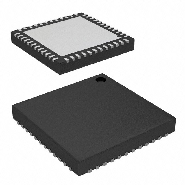


 工商网监
湘ICP备2023018690号
工商网监
湘ICP备2023018690号
