PRELIMINARY
CY2XF32
High Performance CMOS Oscillator with Frequency Margining - Pin Control
Features
■ ■ ■ ■ ■ ■ ■ ■ ■
Functional Description
The CY2XF32 is a high performance and high frequency Crystal Oscillator (XO). It uses a Cypress proprietary low noise PLL to synthesize the frequency from an integrated crystal. The output frequency can be changed via two select pins, allowing easy frequency margin testing in applications. The CY2XF32 is available as a factory configured device or as a field programmable device.
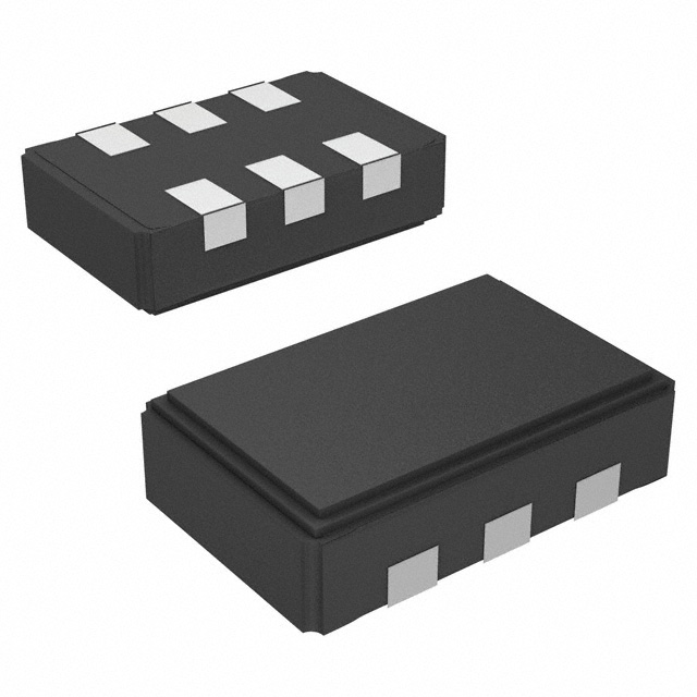
Crystal Oscillator with CMOS Output Output Frequency from 8 MHz to 200 MHz Two Frequency Margining Control Pins (FS0, FS1) Output Enable or Power Down Function Factory Configured or Field Programmable Integrated Phase-Locked Loop (PLL) Supply Voltage: 3.3V or 2.5V Pb-free Package: 5.0 x 3.2 mm LCC Commercial and Industrial Temperature Ranges
Logic Block Diagram
CRYSTAL OSCILLATOR
LOW -NOISE PLL
OUTPU T DIVIDER
4
CLK
FS1
2
FREQUENCY SELECT DECODE
FS0
5
OE/PD#
1
Pinouts
Figure 1. Pin Diagram - 6 Pin Ceramic LCC
OE/PD# 1 FS1 2 VSS 3 6 VDD 5 FS0 4 CLK
Cypress Semiconductor Corporation Document Number: 001-53147 Rev. *B
•
198 Champion Court
•
San Jose, CA 95134-1709 • 408-943-2600 Revised September 18, 2009
[+] Feedback
�PRELIMINARY
CY2XF32
Table 1. Pin Definitions - 6 Pin Ceramic LCC Pin 1 2, 5 4 6 3 Name OE/PD# FS1, FS0 CLK VDD VSS I/O Type CMOS Input CMOS Input CMOS Output Power Power Description Output Enable or Power Down: Functionality is a programming option; see Table 3 and Table 4 for details. Frequency Select. Clock Output. Supply Voltage: 2.5V or 3.3V. Ground. Table 4. Power Down Operation PD# 0 1 PLL & Xtal Oscillator Off Active Output Buffer Off On
Functional Description
The FS0 and FS1 pins select between four different output frequencies, as shown in Table 2. Frequency margining is a common application for this feature. One frequency is used for the standard operating mode of the device, while the other frequencies are available for margin testing, either during product development or in system manufacturing test. Table 2. Frequency Select FS1 0 0 1 1 FS0 0 1 0 1 Output Frequency Frequency 0 Frequency 1 Frequency 2 Frequency 3
Programming Description
The CY2XF32 is a programmable device. Before being used in an application, it must be programmed with the output frequencies and other variables described in a later section. Two different device types are available, each with its own programming flow. They are described below.
Field Programmable CY2XF32F
Field programmable devices are shipped unprogrammed and must be programmed before being installed on a printed circuit board (PCB). Customers use CyberClocks™ Online Software to specify the device configuration and generate a JEDEC (extension .jed) programming file. Programming of samples and prototype quantities is available using a Cypress programmer. Third party vendors manufacture programmers for small to large volume applications. Cypress’s value added distribution partners also provide programming services. Field programmable devices are designated with an “F” in the part number. They are intended for quick prototyping and inventory reduction. The CY2XF32 is one time programmable (OTP). The software is located at www.cyberclocksonline.com.
When changing the output frequency, the frequency transition is not guaranteed to be smooth. There can be frequency excursions beyond the start frequency and the new frequency. Glitches and runt pulses are possible, and time must be allowed for the PLL to relock. Pin 1 is programmed to function as either OE (output enable) or PD# (power down, active low). The OE function is used to enable or disable the CLK output very quickly, but it does not reduce core power consumption. The PD# function puts the device into a low power state, but the wake up takes longer because the PLL must reacquire lock. Details are shown in Table 3 and Table 4. Table 3. Output Enable Operation OE 0 1 PLL & Xtal Oscillator Active Active Output Buffer Off On
Factory Configured CY2XF32
For ready-to-use devices, the CY2XF32 is available with no field programming required. All requests are submitted to the local Cypress Field Application Engineer (FAE) or sales representative. After the request is processed, the user receives a new part number, samples, and data sheet with the programmed values. This part number is used for additional sample requests and production orders.
Document Number: 001-53147 Rev. *B
Page 2 of 8
[+] Feedback
�PRELIMINARY
CY2XF32
Programming Variables
Output Frequencies
The CY2XF32 is programmed with up to four independent output frequencies, which are then selected using the FS0 and FS1 pins. The device can synthesize frequencies to a resolution of one part per million (ppm), but the actual accuracy of the output frequency is limited by the accuracy of the integrated reference crystal.
Industrial versus Commercial Device Performance
Industrial and commercial devices have different internal crystals. This has a potentially significant impact on performance levels for applications requiring the lowest possible phase noise. CyberClocks Online Software displays expected performance for both options. Table 5. Device Programming Variables Variable Output Frequency 0 (Power on default) Output Frequency 1 Output Frequency 2 Output Frequency 3 Pin 1 Functionality (OE or PD#) Supply Voltage (2.5V or 3.3V) Temperature Range (Commercial or Industrial)
Pin 1: Output Enable or Power Down (OE/PD#)
Pin 1 is programmed as either Output Enable (OE) or Power Down (PD#).
Supply Voltage
A programming option optimizes the CY2XF32 for either 2.5V or 3.3V supply voltage. A device programmed for a particular supply voltage is not guaranteed to meet specifications when operated at the other voltage.
Document Number: 001-53147 Rev. *B
Page 3 of 8
[+] Feedback
�PRELIMINARY
CY2XF32
Absolute Maximum Conditions
Parameter VDD VIN[1] TS TJ ESDHBM ΘJA[2] Supply Voltage Input Voltage, DC Temperature, Storage Temperature, Junction ESD Protection (Human Body Model) Thermal Resistance, Junction to Ambient JEDEC STD 22-A114-B 0 m/s airflow Relative to VSS Non operating Description Condition Min –0.5 –0.5 –55 –40 2000 64 Max 4.4 VDD+0.5 135 135 – Unit V V °C °C V °C/W
Operating Conditions
Parameter VDD TPU TA CLOAD 3.3V Supply Voltage Range 2.5V Supply Voltage Range Power Up Time for VDD to Reach Minimum Specified Voltage (Power Ramp is Monotonic) Ambient Temperature, Commercial Ambient Temperature, Industrial Load Capacitance at CLK (>100 MHz) Load Capacitance at CLK (≤100 MHz) Description Min 3.135 2.375 0.05 0 –40 – – Typ 3.3 2.5 – – – – – Max 3.465 2.625 500 70 85 10 15 Unit V V ms °C °C pF pF
DC Electrical Characteristics
Parameter IDD ISB VOH VOL IOZ VIH VIL IIH0 IIH1 IIL0 IIL1 CIN0[3] CIN1[3] Description Operating Supply Current Standby Supply Current Output High Voltage Output Low Voltage Output Leakage Current Input High Voltage Input Low Voltage Input High Current, OE/PD# Pin Input Low Current, OE/PD# Pin Input Low Current, FS0 & FS1 Pin Input Capacitance, OE/PD# Pin Input Capacitance, FS0 & FS1 Pin Input = VDD Input = VSS Input = VSS Input High Current, FS0 & FS1 Pins Input = VDD Condition VDD = 3.465V, OE/PD# = VDD, output unloaded PD# = VSS VDD = min, IOH = –4 mA VDD = max, IOL = 4 mA OE/PD# = VSS Min – – 0.9*VDD – –35 0.7*VDD – – – –50 –20 – – Typ – – – – – – – – – – – 15 4 Max 110 200 – 0.1*VDD 35 – 0.3*VDD 115 10 – – – – Unit mA μA V V μA V V μA μA μA μA pF pF
Notes 1. The voltage on any input or I/O pin cannot exceed the power pin during power up. 2. Simulated. The board is derived from the JEDEC multilayer standard. It measures 76 x 114 x 1.6 mm and has four layers of copper (2/1/1/2 oz.). The internal layers are 100% copper planes, while the top and bottom layers have 50% metalization. No vias are included in the model. 3. Not 100% tested, guaranteed by design and characterization.
Document Number: 001-53147 Rev. *B
Page 4 of 8
[+] Feedback
�PRELIMINARY
AC Electrical Characteristics[3]
Parameter FOUT FSC FSI AG TDC TR TF TOHZ TOE TLOCK TLFS Description Output Frequency[5] Frequency Stability, Commercial Devices[4] Frequency Stability, Industrial Devices[4] Aging, 10 Years Output Duty Cycle Output Rise Time Output Fall Time Output Disable Time Output Enable Time Startup Time Measured at VDD/2; see Figure 2 20% to 80% of VDD, CLOAD = 15 pF 80% to 20% of VDD, CLOAD = 15 pF Time from falling edge on OE to stopped outputs (Asynchronous) Time from rising edge on OE to outputs at a valid frequency (Asynchronous) Time for CLK to reach valid frequency measured from the time VDD = VDD(min.) or from PD# rising edge Time for CLK to reach valid frequency from FS0 or FS1 pin change TA = 0°C to 70°C TA = –40°C to 85°C Condition Min 8 – – – 45 – – – – – Typ – – – – 50 0.7 0.8 – – –
CY2XF32
Max 200 ±35 ±55 ±15 55 1.5 1.5 100 100 5
Unit MHz ppm ppm ppm % ns ns ns ns ms
Relock Time
–
–
1
ms
Notes 4. Frequency stability is the maximum variation in frequency from F0. It includes initial accuracy, plus variation from temperature and supply voltage. 5. This parameter is specified in CyberClocks Online software.
Document Number: 001-53147 Rev. *B
Page 5 of 8
[+] Feedback
�PRELIMINARY
CY2XF32
Switching Waveforms
Figure 2. Duty Cycle Timing
CLK TPW
TDC = TPERIOD
TPW TPERIOD
Figure 3. Output Rise and Fall Time
CLK 20%
80%
80% 20%
VDD
0V TR TF
Figure 4. Output Enable and Disable Timing
OE
V IL
V IH
TOH Z
TOE
CLK
High Impedance
Document Number: 001-53147 Rev. *B
Page 6 of 8
[+] Feedback
�PRELIMINARY
CY2XF32
Ordering Information
Part Number[6] Pb-Free CY2XF32FLXCT CY2XF32FLXIT CY2XF32LXCxxxT CY2XF32LXIxxxT Field Programmable Field Programmable Factory Configured Factory Configured 6-Pin Ceramic LCC SMD - Tape and Reel 6-Pin Ceramic LCC SMD - Tape and Reel 6-Pin Ceramic LCC SMD - Tape and Reel 6-Pin Ceramic LCC SMD - Tape and Reel Commercial, 0° to 70°C Industrial, –40° to 85°C Commercial, 0° to 70°C Industrial, –40° to 85°C Configuration Package Description Product Flow
Package Diagram
Figure 5. 6-Pin 3.2x5.0 mm Ceramic LCC
0.50
SIDE VIEW
1.30 Max
2.54 TYP. 0.64 TYP.
0.10 R REF. TYP. TYP. 0.20 R REF.
4 5 6
5.0
0.32 R INDEX
7
10
TYP.
9 8 3 2 1
TOP VIEW BOTTOM VIEW
Dimensions in mm General Tolerance: ± 0.15MM Kyocera dwg ref KD-VA6432-A Package Weight ~ 0.12 grams
001-10044-**
.
Note 6. “xxx” is a factory assigned code that identifies the programming option.
Document Number: 001-53147 Rev. *B
0.10 REF.
Page 7 of 8
0.45 REF.
1.27
[+] Feedback
3.2
1.2 TYP.
�PRELIMINARY
CY2XF32
Document History Page
Document Title: CY2XF32 High Performance CMOS Oscillator with Frequency Margining - Pin Control Document Number: 001-53147 Rev. ** *A *B ECN No. 2705753 2734005 2764787 Orig. of Change KVM/PYRS WWZ KVM Submission Date 05/13/09 New data sheet 07/09/2009 Post to external web 09/19/2009 Change ISB max from 250 μA to 200 μA Add max limit for TR, TF: 1.5 ns Change TLOCK max from 10 ms to 5 ms Change TLFS max from 10 ms to 1 ms Description of Change
Sales, Solutions, and Legal Information
Worldwide Sales and Design Support
Cypress maintains a worldwide network of offices, solution centers, manufacturer’s representatives, and distributors. To find the office closest to you, visit us at cypress.com/sales.
Products
PSoC Clocks & Buffers Wireless Memories Image Sensors psoc.cypress.com clocks.cypress.com wireless.cypress.com memory.cypress.com image.cypress.com
© Cypress Semiconductor Corporation, 2009. The information contained herein is subject to change without notice. Cypress Semiconductor Corporation assumes no responsibility for the use of any circuitry other than circuitry embodied in a Cypress product. Nor does it convey or imply any license under patent or other rights. Cypress products are not warranted nor intended to be used for medical, life support, life saving, critical control or safety applications, unless pursuant to an express written agreement with Cypress. Furthermore, Cypress does not authorize its products for use as critical components in life-support systems where a malfunction or failure may reasonably be expected to result in significant injury to the user. The inclusion of Cypress products in life-support systems application implies that the manufacturer assumes all risk of such use and in doing so indemnifies Cypress against all charges. Any Source Code (software and/or firmware) is owned by Cypress Semiconductor Corporation (Cypress) and is protected by and subject to worldwide patent protection (United States and foreign), United States copyright laws and international treaty provisions. Cypress hereby grants to licensee a personal, non-exclusive, non-transferable license to copy, use, modify, create derivative works of, and compile the Cypress Source Code and derivative works for the sole purpose of creating custom software and or firmware in support of licensee product to be used only in conjunction with a Cypress integrated circuit as specified in the applicable agreement. Any reproduction, modification, translation, compilation, or representation of this Source Code except as specified above is prohibited without the express written permission of Cypress. Disclaimer: CYPRESS MAKES NO WARRANTY OF ANY KIND, EXPRESS OR IMPLIED, WITH REGARD TO THIS MATERIAL, INCLUDING, BUT NOT LIMITED TO, THE IMPLIED WARRANTIES OF MERCHANTABILITY AND FITNESS FOR A PARTICULAR PURPOSE. Cypress reserves the right to make changes without further notice to the materials described herein. Cypress does not assume any liability arising out of the application or use of any product or circuit described herein. Cypress does not authorize its products for use as critical components in life-support systems where a malfunction or failure may reasonably be expected to result in significant injury to the user. The inclusion of Cypress’ product in a life-support systems application implies that the manufacturer assumes all risk of such use and in doing so indemnifies Cypress against all charges. Use may be limited by and subject to the applicable Cypress software license agreement.
Document Number: 001-53147 Rev. *B
Revised September 18, 2009
Page 8 of 8
CyberClocks is a trademark of Cypress Semiconductor Corporation. All products and company names mentioned in this document may be the trademarks of their respective holders.
[+] Feedback
�


 工商网监
湘ICP备2023018690号
工商网监
湘ICP备2023018690号
