CY7C419/21/25/29/33256/512/1K/2K/4K x 9 Asynchronous FIFO
CY7C419/21/25/29/33
256/512/1K/2K/4K x 9 Asynchronous FIFO
Features
Functional Description
■
Asynchronous First-In First-Out (FIFO) Buffer Memories
❐ 256 x 9 (CY7C419)
❐ 512 x 9 (CY7C421)
❐ 1K x 9 (CY7C425)
❐ 2K x 9 (CY7C429)
❐ 4K x 9 (CY7C433)
■
Dual-Ported RAM Cell
■
High Speed 50 MHz Read and Write Independent of Depth and
Width
■
Low Operating Power: ICC = 35 mA
■
Empty and Full Flags (Half Full Flag in Standalone)
■
TTL Compatible
■
Retransmit in Standalone
■
Expandable in Width
■
PLCC, 7x7 TQFP, SOJ, 300-mil, and 600-mil DIP
■
Pb-free Packages Available
■
Pin Compatible and Functionally Equivalent to IDT7200,
IDT7201, IDT7202, IDT7203, IDT7204, AM7200, AM7201,
AM7202, AM7203, and AM7204
The CY7C419, CY7C420/1, CY7C424/5, CY7C428/9, and
CY7C432/3 are first-in first-out (FIFO) memories offered in
600-mil wide and 300-mil wide packages. There are 256, 512,
1,024, 2,048, and 4,096 words respectively by 9 bits wide. Each
FIFO memory is organized such that the data is read in the same
sequential order that it was written. Full and empty flags are
provided to prevent overrun and underrun. Three additional pins
are also provided to facilitate unlimited expansion in width, depth,
or both. The depth expansion technique steers the control
signals from one device to another in parallel. This eliminates the
serial addition of propagation delays, so that throughput is not
reduced. Data is steered in a similar manner.
The read and write operations may be asynchronous; each can
occur at a rate of 50 MHz. The write operation occurs when the
write (W) signal is LOW. Read occurs when read (R) goes LOW.
The nine data outputs go to the high impedance state when R is
HIGH.
A Half Full (HF) output flag that is valid in the standalone and
width expansion configurations is provided. In the depth
expansion configuration, this pin provides the expansion out
(XO) information that is used to tell the next FIFO that it is
activated.
In the standalone and width expansion configurations, a LOW on
the retransmit (RT) input causes the FIFOs to retransmit the
data. Read enable (R) and write enable (W) must both be HIGH
during retransmit, and then R is used to access the data.
The CY7C419, CY7C420, CY7C421, CY7C424, CY7C425,
CY7C428, CY7C429, CY7C432, and CY7C433 are fabricated
using an advanced 0.65-micron P-well CMOS technology. Input
ESD protection is greater than 2000V and latch up is prevented
by careful layout and guard rings.
Table 1. Selection Guide
4K x 9
–10
–15
–20
–25
–30
–40
–65
Frequency (MHz)
50
40
33.3
28.5
25
20
12.5
Maximum Access Time (ns)
10
15
20
25
30
40
65
ICC1 (mA)
35
35
35
35
35
35
35
Cypress Semiconductor Corporation
Document #: 38-06001 Rev. *D
•
198 Champion Court
•
San Jose, CA 95134-1709
•
408-943-2600
Revised June 03, 2009
[+] Feedback
�CY7C419/21/25/29/33
Logic Block Diagram
DATA INPUTS
(D0–D 8)
W
WRITE
CONTROL
RAM ARRAY
256 x 9
512 x 9
1024x 9
2048x 9
4096x 9
WRITE
POINTER
READ
POINTER
THREESTATE
BUFFERS
DATA OUTPUTS
(Q0–Q 8)
R
FLAG
LOGIC
XI
MR
RESET
LOGIC
READ
CONTROL
EXPANSION
LOGIC
FL/RT
EF
FF
XO/HF
Pin Configurations
XO/HF
Q7
Q6
32 3130 29 28 27 26 25
D1
D0
NC
NC
XI
FF
Q0
Q1
1
2
3
4
5
6
7
8
Document #: 38-06001 Rev. *D
24
23
22
21
20
19
18
17
7C419
7C421/5/9
7C433
D7
FL/RT
NC
NC
MR
EF
XO/HF
Q7
9 10 11 12 13 14 15 16
Q2
Q3
Q8
GND
R
Q4
Vcc
D4
D5
D6
D7
FL/RT
MR
EF
XO/HF
Q7
Q6
Q5
Q4
R
Q6
D6
D7
NC
FL/RT
MR
EF
28
1
27
2
26
3
4
25
5
24
7C419
6 7C420/1 23
7 7C424/5 22
8 7C428/9 21
7C432/3
9
20
10
19
11
18
12
17
13
16
15
14
Q5
D3
D8
W
NC
Vcc
D4
D5
4 3 2 1 323130
5
29
6
28
7
27
8
26
7C419
7C421/5/9 25
9
7C433
10
24
11
23
12
22
13
21
14 15 1617 181920
Q3
Q8
GND
NC
R
Q4
Q5
D2
D1
D0
XI
FF
Q0
Q1
NC
Q2
W
D8
D3
D2
D1
D0
XI
FF
Q0
Q1
Q2
Q3
Q8
GND
D5
D6
Figure 3. 32-PIn TQFP (Top View)
D3
D8
W
VCC
D4
Figure 2. 28-Pin DIP (Top View)
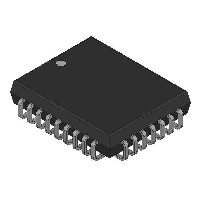
D2
Figure 1. 32-Pin PLCC/LCC (Top View)
Page 2 of 16
[+] Feedback
�CY7C419/21/25/29/33
Maximum Rating
Exceeding maximum ratings may impair the useful life of the
device. These user guidelines are not tested.[1]
Output Current, into Outputs (LOW)............................ 20 mA
Storage Temperature ................................. –65°C to +150°C
Static Discharge Voltage............................................ >2000V
(per MIL–STD–883, Method 3015)
Ambient Temperature with Power Applied.. –55°C to +125°C
Latch Up Current ..................................................... >200 mA
Supply Voltage to Ground Potential................–0.5V to +7.0V
Operating Range
DC Voltage Applied to Outputs
in High Z State ................................................–0.5V to +7.0V
DC Input Voltage ............................................–0.5V to +7.0V
Power Dissipation.......................................................... 1.0W
Range
Ambient Temperature[2]
VCC
0°C to + 70°C
5V ± 10%
–40°C to +85°C
5V ± 10%
Commercial
Industrial
Electrical Characteristics
Over the Operating Range[3]
Parameter
Description
All Speed Grades
Test Conditions
VOH
VOL
VIH
Output HIGH Voltage
Output LOW Voltage
Input HIGH Voltage
VIL
IIX
IOZ
IOS
Input LOW Voltage
Input Leakage Current
Output Leakage Current
Output Short Circuit Current[5]
Min
2.4
VCC = Min., IOH = –2.0 mA
VCC = Min., IOL = 8.0 mA
Commercial
Industrial
V
V
V
0.4
VCC
VCC
0.8
+10
+10
–90
2.0
2.2
[4]
GND < VI < VCC
R > VIH, GND < VO < VCC
VCC = Max., VOUT = GND
Unit
Max
–10
–10
V
μA
μA
mA
Electrical Characteristics
Over the Operating Range
Parameter
Description
Test Conditions
ICC
Operating Current
VCC = Max.,
IOUT = 0 mA
f = fMAX
VCC = Max.,
IOUT = 0 mA
F = 20 MHz
All Inputs =
VIH Min.
ICC1
Operating Current
ISB1
Standby Current
ISB2
Power Down Current All Inputs >
VCC –0.2V
Commercial
Industrial
–10
Min
–15
Max
85
Min
–20
Max
65
100
Min
–25
Max
55
90
Min
Max
50
80
Unit
mA
Commercial
35
35
35
35
mA
Commercial
Industrial
Commercial
Industrial
10
10
15
5
8
10
15
5
8
10
15
5
8
mA
5
mA
Notes
1. Single Power Supply: The voltage on any input or I/O pin cannot exceed the power pin during power up.
2. TA is the “instant on” case temperature.
3. See the last page of this specification for Group A subgroup testing information.
4. VIL (Min.) = –2.0V for pulse durations of less than 20 ns.
5. For test purposes, not more than one output at a time should be shorted. Short circuit test duration should not exceed 30 seconds.
Document #: 38-06001 Rev. *D
Page 3 of 16
[+] Feedback
�CY7C419/21/25/29/33
Electrical Characteristics
Over the Operating Range[3]
Parameter
Description
ICC
Operating Current
ICC1
Operating Current
ISB1
Standby Current
ISB2
Power Down Current
Test Conditions
VCC = Max.,
IOUT = 0 mA
f = fMAX
VCC = Max.,
IOUT = 0 mA
F = 20 MHz
All Inputs =
VIH Min.
All Inputs >
VCC –0.2V
–30
Min
–40
Min
–65
Max
35
70
Min
Max
35
65
Unit
Commercial
Industrial
Max
40
75
Commercial
35
35
35
mA
Commercial
Industrial
Commercial
Industrial
10
15
5
8
10
15
5
8
10
15
5
8
mA
mA
mA
Capacitance
Tested initially and after any design or process changes that may affect these parameters.
Parameter
CIN
COUT
Document #: 38-06001 Rev. *D
Description
Input Capacitance
Output Capacitance
Test Conditions
TA = 25°C, f = 1 MHz,
VCC = 4.5V
Max
6
6
Unit
pF
pF
Page 4 of 16
[+] Feedback
�CY7C419/21/25/29/33
Switching Characteristics
Over the Operating Range[6, 7]
Parameter
tRC
tA
tRR
tPR
tLZR[,8]
tDVR[8,9]
tHZR[,8,9]
tWC
tPW
tHWZ[,8]
tWR
tSD
tHD
tMRSC
tPMR
tRMR
tRPW
tWPW
tRTC
tPRT
tRTR
tEFL
tHFH
tFFH
tREF
tRFF
tWEF
tWFF
tWHF
tRHF
tRAE
tRPE
tWAF
tWPF
tXOL
tXOH
Description
Read Cycle Time
Access Time
Read Recovery Time
Read Pulse Width
Read LOW to Low Z
Data Valid After Read HIGH
Read HIGH to High Z
Write Cycle Time
Write Pulse Width
Write HIGH to Low Z
Write Recovery Time
Data Setup Time
Data Hold Time
MR Cycle Time
MR Pulse Width
MR Recovery Time
Read HIGH to MR HIGH
Write HIGH to MR HIGH
Retransmit Cycle Time
Retransmit Pulse Width
Retransmit Recovery Time
MR to EF LOW
MR to HF HIGH
MR to FF HIGH
Read LOW to EF LOW
Read HIGH to FF HIGH
Write HIGH to EF HIGH
Write LOW to FF LOW
Write LOW to HF LOW
Read HIGH to HF HIGH
Effective Read from Write HIGH
Effective Read Pulse Width After EF HIGH
Effective Write from Read HIGH
Effective Write Pulse Width After FF HIGH
Expansion Out LOW Delay from Clock
Expansion Out HIGH Delay from Clock
–10
Min
20
–15
Max
Min
25
10
10
10
3
5
–20
Max
15
10
15
3
5
15
20
10
5
10
6
0
20
10
10
10
10
20
10
10
15
10
10
10
30
30
30
20
20
20
20
20
20
20
35
35
35
25
25
25
25
25
25
25
25
20
20
15
15
18
35
25
5
10
15
0
35
25
10
25
25
35
25
10
20
15
25
15
15
Max
10
25
3
5
30
20
5
10
12
0
30
20
10
20
20
30
20
10
25
25
25
15
15
15
15
15
15
15
10
Min
35
20
15
20
20
20
10
10
10
10
10
10
10
–25
Max
10
20
3
5
25
15
5
10
8
0
25
15
10
15
15
25
15
10
10
Min
30
25
25
20
20
25
25
Unit
ns
ns
ns
ns
ns
ns
ns
ns
ns
ns
ns
ns
ns
ns
ns
ns
ns
ns
ns
ns
ns
ns
ns
ns
ns
ns
ns
ns
ns
ns
ns
ns
ns
ns
ns
ns
Notes
6. Test conditions assume signal transition time of 3 ns or less, timing reference levels of 1.5V and output loading of the specified IOL/IOH and 30 pF load capacitance,
as in part (a) of AC Test Load and Waveforms, unless otherwise specified.
7. See the last page of this specification for Group A subgroup testing information.
8. tHZR transition is measured at +200 mV from VOL and –200 mV from VOH. tDVR transition is measured at the 1.5V level. tHWZ and tLZR transition is measured at ±100
mV from the steady state.
9. tHZR and tDVR use capacitance loading as in part (b) of AC Test Load and Waveforms.
Document #: 38-06001 Rev. *D
Page 5 of 16
[+] Feedback
�CY7C419/21/25/29/33
Switching Characteristics
Over the Operating Range[6, 7] (continued)
Parameter
Description
–30
Min
–40
Max
–65
Max
Max
tA
Access Time
tRR
Read Recovery Time
10
10
15
ns
tPR
Read Pulse Width
30
40
65
ns
tLZR[,8]
Read LOW to Low Z
3
3
3
ns
Data Valid After Read HIGH
5
30
80
Unit
Read Cycle Time
tDVR
50
Min
tRC
[8,9]
40
Min
40
5
ns
65
5
ns
ns
tHZR[,8,9]
Read HIGH to High Z
tWC
Write Cycle Time
40
50
80
ns
tPW
Write Pulse Width
30
40
65
ns
tHWZ[,8]
Write HIGH to Low Z
5
5
5
ns
tWR
Write Recovery Time
10
10
15
ns
tSD
Data Setup Time
18
20
30
ns
tHD
Data Hold Time
0
0
0
ns
tMRSC
MR Cycle Time
40
50
80
ns
tPMR
MR Pulse Width
30
40
65
ns
tRMR
MR Recovery Time
10
10
15
ns
tRPW
Read HIGH to MR HIGH
30
40
65
ns
tWPW
Write HIGH to MR HIGH
30
40
65
ns
tRTC
Retransmit Cycle Time
40
50
80
ns
tPRT
Retransmit Pulse Width
30
40
65
ns
tRTR
Retransmit Recovery Time
10
10
15
ns
tEFL
MR to EF LOW
40
50
80
ns
tHFH
MR to HF HIGH
40
50
80
ns
tFFH
MR to FF HIGH
40
50
80
ns
tREF
Read LOW to EF LOW
30
35
60
ns
tRFF
Read HIGH to FF HIGH
30
35
60
ns
tWEF
Write HIGH to EF HIGH
30
35
60
ns
tWFF
Write LOW to FF LOW
30
35
60
ns
tWHF
Write LOW to HF LOW
30
35
60
ns
tRHF
Read HIGH to HF HIGH
30
35
60
ns
tRAE
Effective Read from Write HIGH
30
35
60
ns
tRPE
Effective Read Pulse Width After EF HIGH
tWAF
Effective Write from Read HIGH
tWPF
Effective Write Pulse Width After FF HIGH
tXOL
Expansion Out LOW Delay from Clock
30
40
65
ns
tXOH
Expansion Out HIGH Delay from Clock
30
40
65
ns
Document #: 38-06001 Rev. *D
20
30
20
40
30
30
20
65
35
40
ns
ns
60
65
ns
ns
Page 6 of 16
[+] Feedback
�CY7C419/21/25/29/33
Switching Waveforms
Figure 4. Asynchronous Read and Write
tA
R
tRC
tPR
tA
tRR
tLZR
tDVR
tHZR
DATA VALID
Q0–Q 8
tPW
tWC
DATA VALID
tWR
W
tSD
tHD
DATA VALID
D0–D 8
DATA VALID
Figure 5. Master Reset
tMRSC [11]
tPMR
MR
R, W [10]
tRPW
tWPW
tEFL
tRMR
EF
tHFH
HF
tFFH
FF
Figure 6. Half-full Flag
HALF FULL
HALF FULL+1
HALF FULL
W
tRHF
R
tWHF
HF
Notes
10. W and R ≥ VIH around the rising edge of MR
11. tMRSC = tPMR + tRMR.
Document #: 38-06001 Rev. *D
Page 7 of 16
[+] Feedback
�CY7C419/21/25/29/33
Switching Waveforms (continued)
Figure 7. Last Write to First Read Full Flag
R
LAST WRITE
FIRST READ
ADDITIONAL
READS
FIRST WRITE
W
tRFF
tWFF
FF
Figure 8. Last Read to First Write Empty Flag
W
LAST READ
FIRST WRITE
ADDITIONAL
WRITES
FIRST READ
R
tWEF
tREF
EF
tA
DATA OUT
VALID
VALID
Figure 9. Retransmit[12]
tRTC[13]
FL/RT
tPRT
R,W
tRTR
Notes
12. EF, HF and FF may change state during retransmit as a result of the offset of the read and write pointers, but flags are valid at tRTC.
13. tRTC = tPRT + tRTR.
Document #: 38-06001 Rev. *D
Page 8 of 16
[+] Feedback
�CY7C419/21/25/29/33
Switching Waveforms (continued)
Figure 10. Empty Flag and Read Data Flow-through Mode
DATA IN
W
tRAE
R
tREF
EF
tWEF
tHWZ
tRPE
tA
DATA OUT
DATA VALID
Figure 11. Full Flag and Write Data Flow-through Mode
R
tWAF
tWPF
W
tRFF
tWFF
FF
tHD
DATA IN
DATA VALID
tA
DATA OUT
Document #: 38-06001 Rev. *D
tSD
DATA VALID
Page 9 of 16
[+] Feedback
�CY7C419/21/25/29/33
Switching Waveforms (continued)
Figure 12. Expansion Timing Diagrams
WRITE TO LAST PHYSICAL
LOCATION OF DEVICE 1
WRITE TO FIRST PHYSICAL
LOCATION OF DEVICE 2
W
tWR
tXOL
XO1(XI2)[14]
tXOH
tSD
tHD
DATA VALID
D0–D 8
READ FROM LAST PHYSICAL
LOCATION OF DEVICE 1
tHD
tSD
DATA VALID
READ FROM FIRST PHYSICAL
LOCATION OF DEVICE 2
R
tRR
tXOL
[14]
tXOH
XO1(XI2)
tHZR
tLZR
tDVR
tDVR
DATA
VALID
Q0–Q 8
tA
DATA
VALID
tA
Note
14. Expansion Out of device 1 (XO1) is connected to Expansion In of device 2 (XI2)
Document #: 38-06001 Rev. *D
Page 10 of 16
[+] Feedback
�CY7C419/21/25/29/33
Architecture
The CY7C419, CY7C420/1, CY7C424/5, CY7C428/9,
CY7C432/3 FIFOs consist of an array of 256, 512, 1024, 2048,
4096 words of 9 bits each (implemented by an array of dual-port
RAM cells), a read pointer, a write pointer, control signals (W, R,
XI, XO, FL, RT, MR), and Full, Half Full, and Empty flags.
Dual-Port RAM
The dual-port RAM architecture refers to the basic memory cell
used in the RAM. The cell itself enables the read and write operations to be independent of each other, which is necessary to
achieve truly asynchronous operation of the inputs and outputs.
A second benefit is that the time required to increment the read
and write pointers is much less than the time required for data
propagation through the memory, which is the case if memory is
implemented using the conventional register array architecture.
Resetting the FIFO
Upon power up, the FIFO must be reset with a Master Reset
(MR) cycle. This causes the FIFO to enter the empty condition
signified by the Empty flag (EF) being LOW, and both the Half
Full (HF) and Full flags (FF) being HIGH. Read (R) and write (W)
must be HIGH tRPW/tWPW before and tRMR after the rising edge
of MR for a valid reset cycle. If reading from the FIFO after a reset
cycle is attempted, the outputs are in the high impedance state.
Writing Data to the FIFO
The availability of at least one empty location is indicated by a
HIGH FF. The falling edge of W initiates a write cycle. Data
appearing at the inputs (D0–D8) tSD before and tHD after the
rising edge of W are stored sequentially in the FIFO.
The EF LOW-to-HIGH transition occurs tWEF after the first
LOW-to-HIGH transition of W for an empty FIFO. HF goes LOW
tWHF after the falling edge of W following the FIFO actually being
Half Full. Therefore, the HF is active after the FIFO is filled to half
its capacity plus one word. HF remains LOW while less than one
half of total memory is available for writing. The LOW-to-HIGH
transition of HF occurs tRHF after the rising edge of R when the
FIFO goes from half full +1 to half full. HF is available in
standalone and width expansion modes. FF goes LOW tWFF
after the falling edge of W, during the cycle in which the last
available location is filled. Internal logic prevents overrunning a
full FIFO. Writes to a full FIFO are ignored and the write pointer
is not incremented. FF goes HIGH tRFF after a read from a full
FIFO.
Reading Data from the FIFO
The falling edge of R initiates a read cycle if the EF is not LOW.
Data outputs (Q0 to Q8) are in a high impedance condition
between read operations (R HIGH), when the FIFO is empty, or
when the FIFO is not the active device in the depth expansion
mode.
When one word is in the FIFO, the falling edge of R initiates a
HIGH-to-LOW transition of EF. The rising edge of R causes the
data outputs to go to the high impedance state and remain such
until a write is performed. Reads to an empty FIFO are ignored
and do not increment the read pointer. From the empty condition,
the FIFO can be read tWEF after a valid write.
The retransmit feature is beneficial when transferring packets of
data. It enables the receiver to acknowledge receipt of data and
retransmit, if necessary.
The Retransmit (RT) input is active in the standalone and width
expansion modes. The retransmit feature is intended for use
when a number of writes equal to or less than the depth of the
FIFO have occurred since the last MR cycle. A LOW pulse on RT
resets the internal read pointer to the first physical location of the
FIFO. R and W must both be HIGH while and tRTR after
retransmit is LOW. With every read cycle after retransmit, previously accessed data and not previously accessed data is read
and the read pointer is incremented until it is equal to the write
pointer. Full, Half Full, and Empty flags are governed by the
relative locations of the read and write pointers and are updated
during a retransmit cycle. Data written to the FIFO after activation
of RT are also transmitted. FIFO, up to the full depth, can be
repeatedly retransmitted.
Standalone/Width Expansion Modes
Standalone and width expansion modes are set by grounding
Expansion In (XI) and tying First Load (FL) to VCC. FIFOs can be
expanded in width to provide word widths greater than nine in
increments of nine. During width expansion mode, all control line
inputs are common to all devices, and flag outputs from any
device can be monitored.
Depth Expansion Mode
Depth expansion mode (see Figure on page 12) is entered
when, during a MR cycle, Expansion Out (XO) of one device is
connected to Expansion In (XI) of the next device, with XO of the
last device connected to XI of the first device. In the depth
expansion mode the First Load (FL) input, when grounded,
indicates that this part is the first to be loaded. All other devices
must have this pin HIGH. To enable the correct FIFO, XO is
pulsed LOW when the last physical location of the previous FIFO
is written to and pulsed LOW again when the last physical
location is read. Only one FIFO is enabled for read and one for
write at any particular time. All other devices are in standby.
FIFOs can also be expanded simultaneously in depth and width.
Consequently, any depth or width FIFO can be created of word
widths in increments of 9. When expanding in depth, a composite
FF must be created by ORing the FFs together. Likewise, a
composite EF is created by ORing the EFs together. HF and RT
functions are not available in depth expansion mode.
Document #: 38-06001 Rev. *D
Page 11 of 16
[+] Feedback
�CY7C419/21/25/29/33
Use of the Empty and Full Flags
For example, consider an empty FIFO that is receiving read
pulses. Because the FIFO is empty, the read pulses are ignored
by the FIFO, and nothing happens. Next, a single word is written
into the FIFO, with a signal that is asynchronous to the read
signal. The (internal) state machine in the FIFO goes from empty
to empty+1. However, it does this asynchronously with respect
to the read signal, so that the effective pulse width of the read
signal cannot be determined, because the state machine does
not look at the read signal until it goes to the empty+1 state.
Similarly, the minimum write pulse width may be violated by
trying to write into a full FIFO, and asynchronously performing a
read. The empty and full flags are used to avoid these effective
pulse width violations, but to do this and operate at the maximum
frequency, the flag must be valid at the beginning of the next
cycle.
To achieve maximum frequency, the flags must be valid at the
beginning of the next cycle. However, because they can be
updated by either edge of the read or write signal, they must be
valid by one-half of a cycle. Cypress FIFOs meet this
requirement; some competitors’ FIFOs do not.
The reason for why the flags should be valid by the next cycle is
complex. The “effective pulse width violation” phenomenon can
occur at the full and empty boundary conditions, if the flags are
not properly used. The empty flag must be used to prevent
reading from an empty FIFO and the full flag must be used to
prevent writing into a full FIFO.
Figure 13. Depth Expansion
XO
R
W
FF
9
EF
CY7C419
CY7C420/1
CY7C424/5
CY7C428/9
CY7C432/3
9
D
9
Q
FL
VCC
XI
XO
FULL
FF
EF
CY7C419
CY7C420/1
CY7C424/5
CY7C428/9
CY7C432/3
9
EMPTY
FL
XI
XO
*
FF
9
MR
CY7C419
CY7C420/1
CY7C424/5
CY7C428/9
CY7C432/3
EF
FL
XI
* FIRST DEVICE
Document #: 38-06001 Rev. *D
Page 12 of 16
[+] Feedback
�CY7C419/21/25/29/33
Ordering Information
Speed
(ns)
10
15
20
25
30
40
65
Package
Diagram
Package Type
CY7C421–10AC
51-85063
32-Pin Thin Plastic Quad Flatpack
CY7C421–10JC
51-85002
32-Pin Plastic Leaded Chip Carrier
CY7C421–10JXC
51-85002
32-Pin Plastic Leaded Chip Carriers (Pb-free)
CY7C421–10PC
51-85014
28-Pin (300-Mil) Molded DIP
CY7C421–10VC
51-85031
28-Pin (300-Mil) Molded SOJ
CY7C421–15AC
51-85063
32-Pin Thin Plastic Quad Flatpack
CY7C421–15AXC
51-85063
32-Pin Thin Plastic Quad Flatpack (Pb-free)
CY7C421–15JC
51-85002
32-Pin Plastic Leaded Chip Carrier
CY7C421–15JI
51-85002
32-Pin Plastic Leaded Chip Carrier
CY7C421–15VI
51-85031
28-Pin (300-Mil) Molded SOJ
CY7C421–20JC
51-85002
32-Pin Plastic Leaded Chip Carrier
CY7C421–20JXC
51-85002
32-Pin Plastic Leaded Chip Carriers (Pb-free)
CY7C421–20PC
51-85014
28-Pin (300-Mil) Molded DIP
CY7C421–20VC
51-85031
28-Pin (300-Mil) Molded SOJ
CY7C421–20VXC
51-85031
28-Pin (300-Mil) Molded SOJ (Pb-free)
CY7C421–20JI
51-85002
32-Pin Plastic Leaded Chip Carrier
CY7C421–20JXI
51-85002
32-Pin Plastic Leaded Chip Carrier (Pb-free)
CY7C421–25JC
51-85002
32-Pin Plastic Leaded Chip Carrier
CY7C421–25PC
51-85014
28-Pin (300-Mil) Molded DIP
CY7C421–25VC
51-85031
28-Pin (300-Mil) Molded SOJ
CY7C421–25JI
51-85002
32-Pin Plastic Leaded Chip Carrier
CY7C421–25PI
51-85014
28-Pin (300-Mil) Molded DIP
CY7C421–30JC
51-85002
32-Pin Plastic Leaded Chip Carrier
CY7C421–30PC
51-85014
28-Pin (300-Mil) Molded DIP
CY7C421–30JI
51-85002
32-Pin Plastic Leaded Chip Carrier
Industrial
CY7C421–40JC
51-85002
32-Pin Plastic Leaded Chip Carrier
Commercial
CY7C421–40PC
51-85014
28-Pin (300-Mil) Molded DIP
CY7C421–40VC
51-85031
28-Pin (300-Mil) Molded SOJ
CY7C421–40JI
51-85002
32-Pin Plastic Leaded Chip Carrier
Industrial
CY7C421–65JC
51-85002
32-Pin Plastic Leaded Chip Carrier
Commercial
CY7C421–65PC
51-85014
28-Pin (300-Mil) Molded DIP
CY7C421–65VC
51-85031
28-Pin (300-Mil) Molded SOJ
CY7C421–65JI
51-85002
32-Pin Plastic Leaded Chip Carrier
Ordering Code
Document #: 38-06001 Rev. *D
Operating
Range
Commercial
Commercial
Industrial
Commercial
Industrial
Commercial
Industrial
Commercial
Industrial
Page 13 of 16
[+] Feedback
�CY7C419/21/25/29/33
Package Diagrams
Figure 14. 32-Pin Thin Plastic Quad Flat Pack, 51-85063
51-85063-*B
Figure 15. 32-Pin Plastic Leaded Chip Carrier, 51-85002
51-85002-*B
Document #: 38-06001 Rev. *D
Page 14 of 16
[+] Feedback
�CY7C419/21/25/29/33
Package Diagrams
Figure 16. 28-Pin (300-Mil) PDIP, 51-85014
SEE LEAD END OPTION
14
1
DIMENSIONS IN INCHES [MM] MIN.
MAX.
REFERENCE JEDEC MO-095
0.260[6.60]
0.295[7.49]
15
PACKAGE WEIGHT: 2.15 gms
28
0.030[0.76]
0.080[2.03]
SEATING PLANE
1.345[34.16]
1.385[35.18]
0.290[7.36]
0.325[8.25]
0.120[3.05]
0.140[3.55]
0.140[3.55]
0.190[4.82]
0.115[2.92]
0.160[4.06]
0.015[0.38]
0.060[1.52]
0.009[0.23]
0.012[0.30]
3° MIN.
0.055[1.39]
0.065[1.65]
0.090[2.28]
0.110[2.79]
0.310[7.87]
0.385[9.78]
0.015[0.38]
0.020[0.50]
SEE LEAD END OPTION
LEAD END OPTION
(LEAD #1, 14, 15 & 28)
51-85014-*D
Figure 17. 28-Pin (300-Mil) Molded SOJ, 51-85031
MIN.
MAX.
DIMENSIONS IN INCHES
PIN 1 ID
14
DETAIL
A
EXTERNAL LEAD DESIGN
1
0.291
0.300
15
0.330
0.350
OPTION 1
0.697
0.713
0.014
0.020
OPTION 2
SEATING PLANE
0.120
0.140
0.050
TYP.
0.026
0.032
0.013
0.019
28
A
0.007
0.013
0.004
0.025 MIN.
0.262
0.272
51-85031-*B
Document #: 38-06001 Rev. *D
Page 15 of 16
[+] Feedback
�CY7C419/21/25/29/33
Document History Page
Document Title: CY7C419/21/25/29/33, 256/512/1K/2K/4Kx9 Asynchronous FIFO
Document Number: 38-06001
Rev.
ECN No.
Orig. of
Change
Submission
Date
SZV
07/11/01
Description of Change
**
106462
*A
122332
RBI
12/30/02
Added power up requirements to maximum ratings information.
*B
383597
PCX
See ECN
Added Pb-Free Logo
Added to Part-Ordering Information:
CY7C419–10JXC, CY7C419–15JXC, CY7C419-15VXC,
CY7C421–10JXC, CY7C421–15AXC, CY7C421–20JXC,
CY7C421–20VXC, CY7C425–10AXC, CY7C425–10JXC,
CY7C425–15JXC, CY7C425–20JXC, CY7C425–20VXC,
CY7C429–10AXC, CY7C429–15JXC, CY7C429–20JXC,
CY7C433–10AXC, CY7C433–10JXC, CY7C433–15JXC,
CY7C433–20AXC, CY7C433–20JXC
Added CY7C421-20JXI
Removed CY7C419/25/29/33 from the ordering information table
Removed 26-Lead CerDIP, 32-Lead RLCC, 28-Lead molded DIP
packages from the data sheet
Removed Military Information
*C
2623658
VKN/PYRS
12/17/08
*D
2714768
VKN/AESA
06/04/2009
Change from Spec Number: 38-00079 to 38-06001
Corrected defective Logic Block diagram, Pinouts, and Package diagrams
Sales, Solutions, and Legal Information
Worldwide Sales and Design Support
Cypress maintains a worldwide network of offices, solution centers, manufacturer’s representatives, and distributors. To find the office
closest to you, visit us at cypress.com/sales.
Products
PSoC
Clocks & Buffers
psoc.cypress.com
clocks.cypress.com
Wireless
wireless.cypress.com
Memories
memory.cypress.com
Image Sensors
image.cypress.com
© Cypress Semiconductor Corporation, 2005-2009. The information contained herein is subject to change without notice. Cypress Semiconductor Corporation assumes no responsibility for the use of
any circuitry other than circuitry embodied in a Cypress product. Nor does it convey or imply any license under patent or other rights. Cypress products are not warranted nor intended to be used for
medical, life support, life saving, critical control or safety applications, unless pursuant to an express written agreement with Cypress. Furthermore, Cypress does not authorize its products for use as
critical components in life-support systems where a malfunction or failure may reasonably be expected to result in significant injury to the user. The inclusion of Cypress products in life-support systems
application implies that the manufacturer assumes all risk of such use and in doing so indemnifies Cypress against all charges.
Any Source Code (software and/or firmware) is owned by Cypress Semiconductor Corporation (Cypress) and is protected by and subject to worldwide patent protection (United States and foreign),
United States copyright laws and international treaty provisions. Cypress hereby grants to licensee a personal, non-exclusive, non-transferable license to copy, use, modify, create derivative works of,
and compile the Cypress Source Code and derivative works for the sole purpose of creating custom software and or firmware in support of licensee product to be used only in conjunction with a Cypress
integrated circuit as specified in the applicable agreement. Any reproduction, modification, translation, compilation, or representation of this Source Code except as specified above is prohibited without
the express written permission of Cypress.
Disclaimer: CYPRESS MAKES NO WARRANTY OF ANY KIND, EXPRESS OR IMPLIED, WITH REGARD TO THIS MATERIAL, INCLUDING, BUT NOT LIMITED TO, THE IMPLIED WARRANTIES
OF MERCHANTABILITY AND FITNESS FOR A PARTICULAR PURPOSE. Cypress reserves the right to make changes without further notice to the materials described herein. Cypress does not
assume any liability arising out of the application or use of any product or circuit described herein. Cypress does not authorize its products for use as critical components in life-support systems where
a malfunction or failure may reasonably be expected to result in significant injury to the user. The inclusion of Cypress’ product in a life-support systems application implies that the manufacturer
assumes all risk of such use and in doing so indemnifies Cypress against all charges.
Use may be limited by and subject to the applicable Cypress software license agreement.
Document #: 38-06001 Rev. *D
Revised June 03, 2009
Page 16 of 16
All products and company names mentioned in this document may be the trademarks of their respective holders.
[+] Feedback
�


 工商网监
湘ICP备2023018690号
工商网监
湘ICP备2023018690号
