S25FL127S
128 Mbit (16 Mbyte) MirrorBit® Flash Non-Volatile Memory
CMOS 3.0 Volt Core
Serial Peripheral Interface with Multi-I/O
Data Sheet
S25FL127S Cover Sheet
Notice to Readers: This document states the current technical specifications regarding the Spansion®
product(s) described herein. Each product described herein may be designated as Advance Information,
Preliminary, or Full Production. See Notice On Data Sheet Designations for definitions.
Publication Number S25FL127S_00
Revision 05
Issue Date November 15, 2013
�D at a
S hee t
Notice On Data Sheet Designations
Spansion Inc. issues data sheets with Advance Information or Preliminary designations to advise readers of
product information or intended specifications throughout the product life cycle, including development,
qualification, initial production, and full production. In all cases, however, readers are encouraged to verify
that they have the latest information before finalizing their design. The following descriptions of Spansion data
sheet designations are presented here to highlight their presence and definitions.
Advance Information
The Advance Information designation indicates that Spansion Inc. is developing one or more specific
products, but has not committed any design to production. Information presented in a document with this
designation is likely to change, and in some cases, development on the product may discontinue. Spansion
Inc. therefore places the following conditions upon Advance Information content:
“This document contains information on one or more products under development at Spansion Inc.
The information is intended to help you evaluate this product. Do not design in this product without
contacting the factory. Spansion Inc. reserves the right to change or discontinue work on this proposed
product without notice.”
Preliminary
The Preliminary designation indicates that the product development has progressed such that a commitment
to production has taken place. This designation covers several aspects of the product life cycle, including
product qualification, initial production, and the subsequent phases in the manufacturing process that occur
before full production is achieved. Changes to the technical specifications presented in a Preliminary
document should be expected while keeping these aspects of production under consideration. Spansion
places the following conditions upon Preliminary content:
“This document states the current technical specifications regarding the Spansion product(s)
described herein. The Preliminary status of this document indicates that product qualification has been
completed, and that initial production has begun. Due to the phases of the manufacturing process that
require maintaining efficiency and quality, this document may be revised by subsequent versions or
modifications due to changes in technical specifications.”
Combination
Some data sheets contain a combination of products with different designations (Advance Information,
Preliminary, or Full Production). This type of document distinguishes these products and their designations
wherever necessary, typically on the first page, the ordering information page, and pages with the DC
Characteristics table and the AC Erase and Program table (in the table notes). The disclaimer on the first
page refers the reader to the notice on this page.
Full Production (No Designation on Document)
When a product has been in production for a period of time such that no changes or only nominal changes
are expected, the Preliminary designation is removed from the data sheet. Nominal changes may include
those affecting the number of ordering part numbers available, such as the addition or deletion of a speed
option, temperature range, package type, or VIO range. Changes may also include those needed to clarify a
description or to correct a typographical error or incorrect specification. Spansion Inc. applies the following
conditions to documents in this category:
“This document states the current technical specifications regarding the Spansion product(s)
described herein. Spansion Inc. deems the products to have been in sufficient production volume such
that subsequent versions of this document are not expected to change. However, typographical or
specification corrections, or modifications to the valid combinations offered may occur.”
Questions regarding these document designations may be directed to your local sales office.
2
S25FL127S
S25FL127S_00_05 November 15, 2013
�S25FL127S
128 Mbit (16 Mbyte) MirrorBit® Flash Non-Volatile Memory
CMOS 3.0 Volt Core
Serial Peripheral Interface with Multi-I/O
Data Sheet
Features
Density
Data Retention
– 128 Mbits (16 Mbytes)
– 20 Year Data Retention typical
Serial Peripheral Interface (SPI)
Security features
– SPI Clock polarity and phase modes 0 and 3
– Extended Addressing: 24- or 32-bit address options
– Serial Command set and footprint compatible with S25FL-A,
S25FL-K, and S25FL-P SPI families
– Multi I/O Command set and footprint compatible with
S25FL-P SPI family
– One Time Program (OTP) array of 1024 bytes
– Block Protection:
– Status Register bits to control protection against program or
erase of a contiguous range of sectors.
– Hardware and software control options
– Advanced Sector Protection (ASP)
– Individual sector protection controlled by boot code or password
READ Commands
Spansion® 65 nm MirrorBit Technology with Eclipse™
Architecture
– Normal, Fast, Dual, Quad
– AutoBoot - power up or reset and execute a Normal or Quad read
command automatically at a preselected address
– Common Flash Interface (CFI) data for configuration information.
Supply Voltage: 2.7V to 3.6V
Temperature Range:
Programming (0.8 Mbytes/s)
– Industrial (-40°C to +85°C)
– Automotive In-Cabin (-40°C to +105°C)
– 256- or 512-byte Page Programming buffer options
– Quad-Input Page Programming (QPP) for slow clock systems
Packages (all Pb-free)
Erase (0.5 Mbytes/s)
– Hybrid sector size option - physical set of sixteen 4-kbyte sectors at
top or bottom of address space with all remaining sectors of
64 kbytes
– Uniform sector option - always erase 256-kbyte blocks for software
compatibility with higher density and future devices.
Cycling Endurance
–
–
–
–
8-lead SOIC (208 mil)
16-lead SOIC (300 mil)
8-contact WSON 6 x 5 mm
BGA-24 6 x 8 mm
– 5 x 5 ball (FAB024) and 4 x 6 ball (FAC024) footprint options
– Known Good Die and Known Tested Die
– 100,000 Program-Erase Cycles per sector minimum
Publication Number S25FL127S_00
Revision 05
Issue Date November 15, 2013
This document states the current technical specifications regarding the Spansion product(s) described herein. Spansion Inc. deems the products to have been in sufficient production volume such that subsequent versions of this document are not expected to change. However, typographical or specification corrections, or modifications to the valid combinations offered may occur.
�D at a
1.
S hee t
Performance Summary
Table 1.1 Maximum Read Rates
Clock Rate
(MHz)
Command
Mbytes/s
Read
50
6.25
Fast Read
108
13.5
Dual Read
108
27
Quad Read
108
54
Table 1.2 Typical Program and Erase Rates
Operation
kbytes/s
Page Programming (256-byte page buffer)
650
Page Programming (512-byte page buffer)
800
4-kbyte Physical Sector Erase (Hybrid Sector Option)
30
64-kbyte Physical Sector Erase (Hybrid Sector Option)
500
256-kbyte Logical Sector Erase (Uniform Sector Option)
500
Table 1.3 Current Consumption
Operation
4
Current (mA)
Serial Read 50 MHz
16 (max)
Serial Read 108 MHz
24 (max)
Quad Read 108 MHz
47 (max)
Program
50 (max)
Erase
50 (max)
Standby
0.07 (typ)
S25FL127S
S25FL127S_00_05 November 15, 2013
�Data
She et
Table of Contents
Features
1.
Performance Summary . . . . . . . . . . . . . . . . . . . . . . . . . . . . . . . . . . . . . . . . . . . . . . . . . . . . . . . . . . . . 4
2.
Overview . . . . . . . . . . . . . . . . . . . . . . . . . . . . . . . . . . . . . . . . . . . . . . . . . . . . . . . . . . . . . . . . . . . . . . .
2.1
General Description . . . . . . . . . . . . . . . . . . . . . . . . . . . . . . . . . . . . . . . . . . . . . . . . . . . . . . . .
2.2
Migration Notes . . . . . . . . . . . . . . . . . . . . . . . . . . . . . . . . . . . . . . . . . . . . . . . . . . . . . . . . . . .
2.3
Glossary. . . . . . . . . . . . . . . . . . . . . . . . . . . . . . . . . . . . . . . . . . . . . . . . . . . . . . . . . . . . . . . . .
2.4
Other Resources . . . . . . . . . . . . . . . . . . . . . . . . . . . . . . . . . . . . . . . . . . . . . . . . . . . . . . . . . .
11
11
12
14
15
Hardware Interface
3.
Signal Descriptions . . . . . . . . . . . . . . . . . . . . . . . . . . . . . . . . . . . . . . . . . . . . . . . . . . . . . . . . . . . . . .
3.1
Input/Output Summary. . . . . . . . . . . . . . . . . . . . . . . . . . . . . . . . . . . . . . . . . . . . . . . . . . . . . .
3.2
Address and Data Configuration . . . . . . . . . . . . . . . . . . . . . . . . . . . . . . . . . . . . . . . . . . . . . .
3.3
Hardware Reset (RESET#) . . . . . . . . . . . . . . . . . . . . . . . . . . . . . . . . . . . . . . . . . . . . . . . . . .
3.4
Serial Clock (SCK) . . . . . . . . . . . . . . . . . . . . . . . . . . . . . . . . . . . . . . . . . . . . . . . . . . . . . . . . .
3.5
Chip Select (CS#) . . . . . . . . . . . . . . . . . . . . . . . . . . . . . . . . . . . . . . . . . . . . . . . . . . . . . . . . .
3.6
Serial Input (SI) / IO0 . . . . . . . . . . . . . . . . . . . . . . . . . . . . . . . . . . . . . . . . . . . . . . . . . . . . . . .
3.7
Serial Output (SO) / IO1. . . . . . . . . . . . . . . . . . . . . . . . . . . . . . . . . . . . . . . . . . . . . . . . . . . . .
3.8
Write Protect (WP#) / IO2 . . . . . . . . . . . . . . . . . . . . . . . . . . . . . . . . . . . . . . . . . . . . . . . . . . .
3.9
Hold (HOLD#) / IO3 / RESET# . . . . . . . . . . . . . . . . . . . . . . . . . . . . . . . . . . . . . . . . . . . . . . .
3.10 Voltage Supply (VCC). . . . . . . . . . . . . . . . . . . . . . . . . . . . . . . . . . . . . . . . . . . . . . . . . . . . . . .
3.11 Supply and Signal Ground (VSS) . . . . . . . . . . . . . . . . . . . . . . . . . . . . . . . . . . . . . . . . . . . . . .
3.12 Not Connected (NC) . . . . . . . . . . . . . . . . . . . . . . . . . . . . . . . . . . . . . . . . . . . . . . . . . . . . . . .
3.13 Reserved for Future Use (RFU) . . . . . . . . . . . . . . . . . . . . . . . . . . . . . . . . . . . . . . . . . . . . . . .
3.14 Do Not Use (DNU) . . . . . . . . . . . . . . . . . . . . . . . . . . . . . . . . . . . . . . . . . . . . . . . . . . . . . . . . .
3.15 Block Diagrams . . . . . . . . . . . . . . . . . . . . . . . . . . . . . . . . . . . . . . . . . . . . . . . . . . . . . . . . . . .
16
16
17
17
17
17
18
18
18
18
19
19
19
20
20
20
4.
Signal Protocols . . . . . . . . . . . . . . . . . . . . . . . . . . . . . . . . . . . . . . . . . . . . . . . . . . . . . . . . . . . . . . . . .
4.1
SPI Clock Modes . . . . . . . . . . . . . . . . . . . . . . . . . . . . . . . . . . . . . . . . . . . . . . . . . . . . . . . . . .
4.2
Command Protocol . . . . . . . . . . . . . . . . . . . . . . . . . . . . . . . . . . . . . . . . . . . . . . . . . . . . . . . .
4.3
Interface States . . . . . . . . . . . . . . . . . . . . . . . . . . . . . . . . . . . . . . . . . . . . . . . . . . . . . . . . . . .
4.4
Configuration Register Effects on the Interface . . . . . . . . . . . . . . . . . . . . . . . . . . . . . . . . . . .
4.5
Data Protection . . . . . . . . . . . . . . . . . . . . . . . . . . . . . . . . . . . . . . . . . . . . . . . . . . . . . . . . . . .
22
22
22
26
31
31
5.
Electrical Specifications . . . . . . . . . . . . . . . . . . . . . . . . . . . . . . . . . . . . . . . . . . . . . . . . . . . . . . . . . .
5.1
Absolute Maximum Ratings . . . . . . . . . . . . . . . . . . . . . . . . . . . . . . . . . . . . . . . . . . . . . . . . . .
5.2
Operating Ranges . . . . . . . . . . . . . . . . . . . . . . . . . . . . . . . . . . . . . . . . . . . . . . . . . . . . . . . . .
5.3
Power-Up and Power-Down . . . . . . . . . . . . . . . . . . . . . . . . . . . . . . . . . . . . . . . . . . . . . . . . .
5.4
DC Characteristics . . . . . . . . . . . . . . . . . . . . . . . . . . . . . . . . . . . . . . . . . . . . . . . . . . . . . . . . .
33
33
33
34
36
6.
Timing Specifications . . . . . . . . . . . . . . . . . . . . . . . . . . . . . . . . . . . . . . . . . . . . . . . . . . . . . . . . . . . .
6.1
Key to Switching Waveforms . . . . . . . . . . . . . . . . . . . . . . . . . . . . . . . . . . . . . . . . . . . . . . . . .
6.2
AC Test Conditions . . . . . . . . . . . . . . . . . . . . . . . . . . . . . . . . . . . . . . . . . . . . . . . . . . . . . . . .
6.3
Reset . . . . . . . . . . . . . . . . . . . . . . . . . . . . . . . . . . . . . . . . . . . . . . . . . . . . . . . . . . . . . . . . . . .
6.4
AC Characteristics . . . . . . . . . . . . . . . . . . . . . . . . . . . . . . . . . . . . . . . . . . . . . . . . . . . . . . . . .
37
37
37
38
41
7.
Physical Interface . . . . . . . . . . . . . . . . . . . . . . . . . . . . . . . . . . . . . . . . . . . . . . . . . . . . . . . . . . . . . . . .
7.1
SOIC 8-Lead Package . . . . . . . . . . . . . . . . . . . . . . . . . . . . . . . . . . . . . . . . . . . . . . . . . . . . . .
7.2
SOIC 16-Lead Package . . . . . . . . . . . . . . . . . . . . . . . . . . . . . . . . . . . . . . . . . . . . . . . . . . . . .
7.3
WSON 6x5 Package . . . . . . . . . . . . . . . . . . . . . . . . . . . . . . . . . . . . . . . . . . . . . . . . . . . . . . .
7.4
FAB024 24-Ball BGA Package . . . . . . . . . . . . . . . . . . . . . . . . . . . . . . . . . . . . . . . . . . . . . . .
7.5
FAC024 24-Ball BGA Package . . . . . . . . . . . . . . . . . . . . . . . . . . . . . . . . . . . . . . . . . . . . . . .
44
44
46
48
50
52
Software Interface
8.
Address Space Maps . . . . . . . . . . . . . . . . . . . . . . . . . . . . . . . . . . . . . . . . . . . . . . . . . . . . . . . . . . . . .
8.1
Overview . . . . . . . . . . . . . . . . . . . . . . . . . . . . . . . . . . . . . . . . . . . . . . . . . . . . . . . . . . . . . . . .
8.2
Flash Memory Array. . . . . . . . . . . . . . . . . . . . . . . . . . . . . . . . . . . . . . . . . . . . . . . . . . . . . . . .
8.3
ID-CFI Address Space . . . . . . . . . . . . . . . . . . . . . . . . . . . . . . . . . . . . . . . . . . . . . . . . . . . . . .
8.4
JEDEC JESD216 Serial Flash Discoverable Parameters (SFDP) Space. . . . . . . . . . . . . . .
8.5
OTP Address Space . . . . . . . . . . . . . . . . . . . . . . . . . . . . . . . . . . . . . . . . . . . . . . . . . . . . . . .
8.6
Registers . . . . . . . . . . . . . . . . . . . . . . . . . . . . . . . . . . . . . . . . . . . . . . . . . . . . . . . . . . . . . . . .
November 15, 2013 S25FL127S_00_05
S25FL127S
54
54
54
55
55
55
57
5
�D at a
S hee t
9.
Data Protection . . . . . . . . . . . . . . . . . . . . . . . . . . . . . . . . . . . . . . . . . . . . . . . . . . . . . . . . . . . . . . . . . .
9.1
Secure Silicon Region (OTP). . . . . . . . . . . . . . . . . . . . . . . . . . . . . . . . . . . . . . . . . . . . . . . . .
9.2
Write Enable Command. . . . . . . . . . . . . . . . . . . . . . . . . . . . . . . . . . . . . . . . . . . . . . . . . . . . .
9.3
Block Protection . . . . . . . . . . . . . . . . . . . . . . . . . . . . . . . . . . . . . . . . . . . . . . . . . . . . . . . . . . .
9.4
Advanced Sector Protection . . . . . . . . . . . . . . . . . . . . . . . . . . . . . . . . . . . . . . . . . . . . . . . . .
65
65
65
66
67
10.
Commands . . . . . . . . . . . . . . . . . . . . . . . . . . . . . . . . . . . . . . . . . . . . . . . . . . . . . . . . . . . . . . . . . . . . . 71
10.1 Command Set Summary . . . . . . . . . . . . . . . . . . . . . . . . . . . . . . . . . . . . . . . . . . . . . . . . . . . . 72
10.2 Identification Commands . . . . . . . . . . . . . . . . . . . . . . . . . . . . . . . . . . . . . . . . . . . . . . . . . . . . 76
10.3 Register Access Commands . . . . . . . . . . . . . . . . . . . . . . . . . . . . . . . . . . . . . . . . . . . . . . . . . 79
10.4 Read Memory Array Commands . . . . . . . . . . . . . . . . . . . . . . . . . . . . . . . . . . . . . . . . . . . . . . 88
10.5 Program Flash Array Commands . . . . . . . . . . . . . . . . . . . . . . . . . . . . . . . . . . . . . . . . . . . . . 97
10.6 Erase Flash Array Commands. . . . . . . . . . . . . . . . . . . . . . . . . . . . . . . . . . . . . . . . . . . . . . . 100
10.7 One Time Program Array Commands . . . . . . . . . . . . . . . . . . . . . . . . . . . . . . . . . . . . . . . . . 105
10.8 Advanced Sector Protection Commands . . . . . . . . . . . . . . . . . . . . . . . . . . . . . . . . . . . . . . . 106
10.9 Reset Commands . . . . . . . . . . . . . . . . . . . . . . . . . . . . . . . . . . . . . . . . . . . . . . . . . . . . . . . . 112
10.10 Embedded Algorithm Performance Tables . . . . . . . . . . . . . . . . . . . . . . . . . . . . . . . . . . . . . 114
11.
Software Interface Reference . . . . . . . . . . . . . . . . . . . . . . . . . . . . . . . . . . . . . . . . . . . . . . . . . . . . . 115
11.1 Command Summary . . . . . . . . . . . . . . . . . . . . . . . . . . . . . . . . . . . . . . . . . . . . . . . . . . . . . . 115
12.
Serial Flash Discoverable Parameters (SFDP) Address Map . . . . . . . . . . . . . . . . . . . . . . . . . . . .
12.1 Field Definitions . . . . . . . . . . . . . . . . . . . . . . . . . . . . . . . . . . . . . . . . . . . . . . . . . . . . . . . . . .
12.2 Device ID and Common Flash Interface (ID-CFI) Address Map . . . . . . . . . . . . . . . . . . . . .
12.3 Registers . . . . . . . . . . . . . . . . . . . . . . . . . . . . . . . . . . . . . . . . . . . . . . . . . . . . . . . . . . . . . . .
12.4 Initial Delivery State . . . . . . . . . . . . . . . . . . . . . . . . . . . . . . . . . . . . . . . . . . . . . . . . . . . . . . .
116
117
118
128
130
Ordering Information
6
13.
Ordering Information . . . . . . . . . . . . . . . . . . . . . . . . . . . . . . . . . . . . . . . . . . . . . . . . . . . . . . . . . . . . 131
14.
Contacting Spansion . . . . . . . . . . . . . . . . . . . . . . . . . . . . . . . . . . . . . . . . . . . . . . . . . . . . . . . . . . . . 131
15.
Revision History . . . . . . . . . . . . . . . . . . . . . . . . . . . . . . . . . . . . . . . . . . . . . . . . . . . . . . . . . . . . . . . . 132
S25FL127S
S25FL127S_00_05 November 15, 2013
�Data
She et
Figures
Figure 3.1
Figure 3.2
Figure 3.3
Figure 3.4
Figure 4.1
Figure 4.2
Figure 4.3
Figure 4.4
Figure 4.5
Figure 4.6
Figure 4.7
Figure 4.8
Figure 4.9
Figure 4.10
Figure 5.1
Figure 5.2
Figure 5.3
Figure 5.4
Figure 6.1
Figure 6.2
Figure 6.3
Figure 6.4
Figure 6.5
Figure 6.6
Figure 6.7
Figure 6.8
Figure 6.9
Figure 6.10
Figure 6.11
Figure 6.12
Figure 6.13
Figure 6.14
Figure 6.15
Figure 7.1
Figure 7.2
Figure 7.3
Figure 7.4
Figure 7.5
Figure 7.6
Figure 7.7
Figure 7.8
Figure 7.9
Figure 7.10
Figure 8.1
Figure 9.1
Figure 10.1
Figure 10.2
Figure 10.3
Figure 10.4
Figure 10.5
Figure 10.6
Figure 10.7
Figure 10.8
Figure 10.9
HOLD Mode Operation . . . . . . . . . . . . . . . . . . . . . . . . . . . . . . . . . . . . . . . . . . . . . . . . . . . . .
Bus Master and Memory Devices on the SPI Bus - Single Bit Data Path . . . . . . . . . . . . . . .
Bus Master and Memory Devices on the SPI Bus - Dual Bit Data Path . . . . . . . . . . . . . . . .
Bus Master and Memory Devices on the SPI Bus - Quad Bit Data Path. . . . . . . . . . . . . . . .
SPI Modes Supported . . . . . . . . . . . . . . . . . . . . . . . . . . . . . . . . . . . . . . . . . . . . . . . . . . . . . .
Stand Alone Instruction Command . . . . . . . . . . . . . . . . . . . . . . . . . . . . . . . . . . . . . . . . . . . .
Single Bit Wide Input Command . . . . . . . . . . . . . . . . . . . . . . . . . . . . . . . . . . . . . . . . . . . . . .
Single Bit Wide Output Command . . . . . . . . . . . . . . . . . . . . . . . . . . . . . . . . . . . . . . . . . . . . .
Single Bit Wide I/O Command without Latency . . . . . . . . . . . . . . . . . . . . . . . . . . . . . . . . . . .
Single Bit Wide I/O Command with Latency . . . . . . . . . . . . . . . . . . . . . . . . . . . . . . . . . . . . .
Dual Output Command . . . . . . . . . . . . . . . . . . . . . . . . . . . . . . . . . . . . . . . . . . . . . . . . . . . . .
Quad Output Command without Latency. . . . . . . . . . . . . . . . . . . . . . . . . . . . . . . . . . . . . . . .
Dual I/O Command . . . . . . . . . . . . . . . . . . . . . . . . . . . . . . . . . . . . . . . . . . . . . . . . . . . . . . . .
Quad I/O Command. . . . . . . . . . . . . . . . . . . . . . . . . . . . . . . . . . . . . . . . . . . . . . . . . . . . . . . .
Maximum Negative Overshoot Waveform . . . . . . . . . . . . . . . . . . . . . . . . . . . . . . . . . . . . . . .
Maximum Positive Overshoot Waveform. . . . . . . . . . . . . . . . . . . . . . . . . . . . . . . . . . . . . . . .
Power-up . . . . . . . . . . . . . . . . . . . . . . . . . . . . . . . . . . . . . . . . . . . . . . . . . . . . . . . . . . . . . . . .
Power-down and Voltage Drop . . . . . . . . . . . . . . . . . . . . . . . . . . . . . . . . . . . . . . . . . . . . . . .
Waveform Element Meanings . . . . . . . . . . . . . . . . . . . . . . . . . . . . . . . . . . . . . . . . . . . . . . . .
Input, Output, and Timing Reference Levels . . . . . . . . . . . . . . . . . . . . . . . . . . . . . . . . . . . . .
Test Setup . . . . . . . . . . . . . . . . . . . . . . . . . . . . . . . . . . . . . . . . . . . . . . . . . . . . . . . . . . . . . . .
Reset Low at the End of POR . . . . . . . . . . . . . . . . . . . . . . . . . . . . . . . . . . . . . . . . . . . . . . . .
Reset High at the End of POR . . . . . . . . . . . . . . . . . . . . . . . . . . . . . . . . . . . . . . . . . . . . . . . .
POR followed by Hardware Reset . . . . . . . . . . . . . . . . . . . . . . . . . . . . . . . . . . . . . . . . . . . . .
Separate RESET# Input Initiated Hardware Reset . . . . . . . . . . . . . . . . . . . . . . . . . . . . . . . .
Hardware Reset when Quad Mode is not enabled and IO3 / Reset# is Enabled . . . . . . . . .
Hardware Reset when Quad Mode and IO3 / Reset# are Enabled . . . . . . . . . . . . . . . . . . . .
Clock Timing . . . . . . . . . . . . . . . . . . . . . . . . . . . . . . . . . . . . . . . . . . . . . . . . . . . . . . . . . . . . .
SPI Single Bit Input Timing . . . . . . . . . . . . . . . . . . . . . . . . . . . . . . . . . . . . . . . . . . . . . . . . . .
SPI Single Bit Output Timing . . . . . . . . . . . . . . . . . . . . . . . . . . . . . . . . . . . . . . . . . . . . . . . . .
SPI MIO Timing . . . . . . . . . . . . . . . . . . . . . . . . . . . . . . . . . . . . . . . . . . . . . . . . . . . . . . . . . . .
Hold Timing . . . . . . . . . . . . . . . . . . . . . . . . . . . . . . . . . . . . . . . . . . . . . . . . . . . . . . . . . . . . . .
WP# Input Timing . . . . . . . . . . . . . . . . . . . . . . . . . . . . . . . . . . . . . . . . . . . . . . . . . . . . . . . . .
8-pin Plastic Small Outline Package (SO) . . . . . . . . . . . . . . . . . . . . . . . . . . . . . . . . . . . . . . .
S0C008 — 8-Lead Plastic Small Outline Package (208-mil Body Width) . . . . . . . . . . . . . . .
16-Lead SOIC Package, Top View . . . . . . . . . . . . . . . . . . . . . . . . . . . . . . . . . . . . . . . . . . . .
S03016 — 16-Lead Wide Plastic Small Outline Package (300-mil Body Width) . . . . . . . . . .
8-Contact WSON 6x5 mm, Top View . . . . . . . . . . . . . . . . . . . . . . . . . . . . . . . . . . . . . . . . . .
WND008 — WSON 8-contact (6 x 5 mm) No-Lead Package . . . . . . . . . . . . . . . . . . . . . . . .
24-Ball BGA, 5 x 5 Ball Footprint (FAB024), Top View . . . . . . . . . . . . . . . . . . . . . . . . . . . . .
FAB024 — 24-ball Ball Grid Array (8 x 6 mm) Package . . . . . . . . . . . . . . . . . . . . . . . . . . . .
24-Ball BGA, 4 x 6 Ball Footprint (FAC024), Top View . . . . . . . . . . . . . . . . . . . . . . . . . . . . .
FAC024 — 24-ball Ball Grid Array (6 x 8 mm) Package . . . . . . . . . . . . . . . . . . . . . . . . . . . .
OTP Address Space . . . . . . . . . . . . . . . . . . . . . . . . . . . . . . . . . . . . . . . . . . . . . . . . . . . . . . .
Advanced Sector Protection Overview . . . . . . . . . . . . . . . . . . . . . . . . . . . . . . . . . . . . . . . . .
READ_ID Command Sequence. . . . . . . . . . . . . . . . . . . . . . . . . . . . . . . . . . . . . . . . . . . . . . .
Read Identification (RDID) Command Sequence . . . . . . . . . . . . . . . . . . . . . . . . . . . . . . . . .
Read Electronic Signature (RES) Command Sequence . . . . . . . . . . . . . . . . . . . . . . . . . . . .
RSFDP Command Sequence . . . . . . . . . . . . . . . . . . . . . . . . . . . . . . . . . . . . . . . . . . . . . . . .
Read Status Register 1 (RDSR1) Command Sequence . . . . . . . . . . . . . . . . . . . . . . . . . . .
Read Status Register 2 (RDSR2) Command . . . . . . . . . . . . . . . . . . . . . . . . . . . . . . . . . . . .
Read Configuration Register (RDCR) Command Sequence . . . . . . . . . . . . . . . . . . . . . . . . .
Read Bank Register (BRRD) Command . . . . . . . . . . . . . . . . . . . . . . . . . . . . . . . . . . . . . . . .
Bank Register Write (BRWR) Command . . . . . . . . . . . . . . . . . . . . . . . . . . . . . . . . . . . . . . . .
November 15, 2013 S25FL127S_00_05
S25FL127S
19
20
20
21
22
24
24
24
24
24
25
25
25
25
33
34
35
35
37
37
37
38
38
38
39
40
40
42
42
42
43
43
43
44
45
46
47
48
49
50
51
52
53
56
67
77
78
78
79
79
80
80
81
81
7
�D at a
Figure 10.10
Figure 10.11
Figure 10.12
Figure 10.13
Figure 10.14
Figure 10.15
Figure 10.16
Figure 10.17
Figure 10.18
Figure 10.19
Figure 10.20
Figure 10.21
Figure 10.22
Figure 10.23
Figure 10.24
Figure 10.25
Figure 10.26
Figure 10.27
Figure 10.28
Figure 10.29
Figure 10.30
Figure 10.31
Figure 10.32
Figure 10.33
Figure 10.34
Figure 10.35
Figure 10.36
Figure 10.37
Figure 10.38
Figure 10.39
Figure 10.40
Figure 10.41
Figure 10.42
Figure 10.43
Figure 10.44
Figure 10.45
Figure 10.46
Figure 10.47
Figure 10.48
Figure 10.49
Figure 10.50
Figure 10.51
Figure 10.52
Figure 10.53
Figure 10.54
Figure 10.55
Figure 10.56
Figure 10.57
Figure 10.58
Figure 10.59
Figure 10.60
Figure 10.61
8
S hee t
BRAC (B9h) Command Sequence . . . . . . . . . . . . . . . . . . . . . . . . . . . . . . . . . . . . . . . . . . . . 82
Write Registers (WRR) Command Sequence – 8 data bits . . . . . . . . . . . . . . . . . . . . . . . . . . 83
Write Registers (WRR) Command Sequence – 16 data bits . . . . . . . . . . . . . . . . . . . . . . . . . 83
Write Registers (WRR 01h) Command Sequence – 24 data bits . . . . . . . . . . . . . . . . . . . . . 83
Write Enable (WREN) Command Sequence . . . . . . . . . . . . . . . . . . . . . . . . . . . . . . . . . . . . . 85
Write Disable (WRDI) Command Sequence . . . . . . . . . . . . . . . . . . . . . . . . . . . . . . . . . . . . . 85
Clear Status Register (CLSR) Command Sequence . . . . . . . . . . . . . . . . . . . . . . . . . . . . . . . 86
AutoBoot Sequence (CR1[1]=0) . . . . . . . . . . . . . . . . . . . . . . . . . . . . . . . . . . . . . . . . . . . . . . 87
AutoBoot Sequence (CR1[1]=1) . . . . . . . . . . . . . . . . . . . . . . . . . . . . . . . . . . . . . . . . . . . . . . 87
AutoBoot Register Read (ABRD) Command . . . . . . . . . . . . . . . . . . . . . . . . . . . . . . . . . . . . . 88
AutoBoot Register Write (ABWR) Command. . . . . . . . . . . . . . . . . . . . . . . . . . . . . . . . . . . . . 88
Read Command Sequence (READ 03h or 13h) . . . . . . . . . . . . . . . . . . . . . . . . . . . . . . . . . . 90
Fast Read (FAST_READ 0Bh or 0Ch) Command Sequence with Read Latency . . . . . . . . . 90
Fast Read Command (FAST_READ 0Bh or 0Ch) Sequence without Read Latency . . . . . . 90
Dual Output Read Command Sequence (3-Byte Address, 3Bh [ExtAdd=0], LC=10b) . . . . . 91
Dual Output Read Command Sequence
(4-Byte Address, 3Ch or 3Bh [ExtAdd=1, LC=10b]) . . . . . . . . . . . . . . . . . . . . . . . . . . . . . . . 91
Dual Output Read Command Sequence
(4-Byte Address, 3Ch or 3Bh [ExtAdd=1, LC=11b]) . . . . . . . . . . . . . . . . . . . . . . . . . . . . . . . 92
Quad Output Read (QOR 6Bh or 4QOR 6Ch) Command Sequence with Read Latency . . . 92
Quad Output Read (QOR 6Bh or 4QOR 6Ch) Command Sequence without Read Latency 93
Dual I/O Read Command Sequence (3-Byte Address, BBh [ExtAdd=0], LC=00b) . . . . . . . . 94
Dual I/O Read Command Sequence (4-Byte Address, BBh [ExtAdd=1], LC=10b) . . . . . . . . 94
Dual I/O Read Command Sequence
(4-Byte Address, BCh or BBh [ExtAdd=1], LC=10b) . . . . . . . . . . . . . . . . . . . . . . . . . . . . . . . 94
Continuous Dual I/O Read Command Sequence
(4-Byte Address, BCh or BBh [ExtAdd=1], LC=10b) . . . . . . . . . . . . . . . . . . . . . . . . . . . . . . . 95
Quad I/O Read Command Sequence (3-Byte Address, EBh [ExtAdd=0], LC=00b) . . . . . . . 96
Continuous Quad I/O Read Command Sequence (3-Byte Address), LC=00b . . . . . . . . . . . 96
Quad I/O Read Command Sequence (4-Byte Address, ECh or EBh [ExtAdd=1], LC=00b) . 97
Continuous Quad I/O Read Command Sequence (4-Byte Address), LC=00b . . . . . . . . . . . 97
Page Program (PP 02h or 4PP 12h) Command Sequence. . . . . . . . . . . . . . . . . . . . . . . . . . 98
Quad Page Program Command Sequence . . . . . . . . . . . . . . . . . . . . . . . . . . . . . . . . . . . . . . 99
Program Suspend Command Sequence . . . . . . . . . . . . . . . . . . . . . . . . . . . . . . . . . . . . . . . 100
Program Resume Command Sequence . . . . . . . . . . . . . . . . . . . . . . . . . . . . . . . . . . . . . . . 100
Parameter Sector Erase (P4E 20h or 4P4E 21h) Command Sequence . . . . . . . . . . . . . . . 101
Sector Erase (SE D8h or 4SE DCh) Command Sequence . . . . . . . . . . . . . . . . . . . . . . . . . 101
Bulk Erase Command Sequence. . . . . . . . . . . . . . . . . . . . . . . . . . . . . . . . . . . . . . . . . . . . . 102
Erase Suspend Command Sequence . . . . . . . . . . . . . . . . . . . . . . . . . . . . . . . . . . . . . . . . . 103
Erase Resume Command Sequence . . . . . . . . . . . . . . . . . . . . . . . . . . . . . . . . . . . . . . . . . 103
OTP Program Command Sequence . . . . . . . . . . . . . . . . . . . . . . . . . . . . . . . . . . . . . . . . . . 105
OTP Read Command Sequence . . . . . . . . . . . . . . . . . . . . . . . . . . . . . . . . . . . . . . . . . . . . . 106
ASPRD Command . . . . . . . . . . . . . . . . . . . . . . . . . . . . . . . . . . . . . . . . . . . . . . . . . . . . . . . . 106
ASPP Command . . . . . . . . . . . . . . . . . . . . . . . . . . . . . . . . . . . . . . . . . . . . . . . . . . . . . . . . . 107
DYBRD Command Sequence . . . . . . . . . . . . . . . . . . . . . . . . . . . . . . . . . . . . . . . . . . . . . . . 107
DYBWR Command Sequence. . . . . . . . . . . . . . . . . . . . . . . . . . . . . . . . . . . . . . . . . . . . . . . 108
PPBRD Command Sequence . . . . . . . . . . . . . . . . . . . . . . . . . . . . . . . . . . . . . . . . . . . . . . . 108
PPBP Command Sequence. . . . . . . . . . . . . . . . . . . . . . . . . . . . . . . . . . . . . . . . . . . . . . . . . 109
PPB Erase Command Sequence. . . . . . . . . . . . . . . . . . . . . . . . . . . . . . . . . . . . . . . . . . . . . 109
PPB Lock Register Read Command Sequence . . . . . . . . . . . . . . . . . . . . . . . . . . . . . . . . . 110
PPB Lock Bit Write Command Sequence . . . . . . . . . . . . . . . . . . . . . . . . . . . . . . . . . . . . . . 110
Password Read Command Sequence. . . . . . . . . . . . . . . . . . . . . . . . . . . . . . . . . . . . . . . . . 111
Password Program Command Sequence . . . . . . . . . . . . . . . . . . . . . . . . . . . . . . . . . . . . . . 111
Password Unlock Command Sequence . . . . . . . . . . . . . . . . . . . . . . . . . . . . . . . . . . . . . . . 112
Software Reset Command Sequence . . . . . . . . . . . . . . . . . . . . . . . . . . . . . . . . . . . . . . . . . 113
Mode Bit Reset Command Sequence . . . . . . . . . . . . . . . . . . . . . . . . . . . . . . . . . . . . . . . . . 113
S25FL127S
S25FL127S_00_05 November 15, 2013
�Data
She et
Tables
Table 1.1
Table 1.2
Table 1.3
Table 2.1
Table 3.1
Table 4.1
Table 4.2
Table 4.3
Table 5.1
Table 5.2
Table 5.3
Table 6.1
Table 6.2
Table 6.3
Table 6.4
Table 6.5
Table 7.1
Table 8.1
Table 8.2
Table 8.3
Table 8.4
Table 8.5
Table 8.6
Table 8.7
Table 8.8
Table 8.9
Table 8.10
Table 8.11
Table 8.12
Table 8.13
Table 8.14
Table 8.15
Table 9.1
Table 9.2
Table 9.3
Table 10.1
Table 10.2
Table 10.3
Table 10.4
Table 10.5
Table 10.6
Table 10.7
Table 10.8
Table 10.9
Table 11.1
Table 12.1
Table 12.2
Table 12.3
Table 12.4
Table 12.5
Table 12.6
Table 12.7
Table 12.8
Table 12.9
Maximum Read Rates . . . . . . . . . . . . . . . . . . . . . . . . . . . . . . . . . . . . . . . . . . . . . . . . . . . . . . . 4
Typical Program and Erase Rates . . . . . . . . . . . . . . . . . . . . . . . . . . . . . . . . . . . . . . . . . . . . . . 4
Current Consumption. . . . . . . . . . . . . . . . . . . . . . . . . . . . . . . . . . . . . . . . . . . . . . . . . . . . . . . . 4
FL Generations Comparison . . . . . . . . . . . . . . . . . . . . . . . . . . . . . . . . . . . . . . . . . . . . . . . . . 12
Signal List . . . . . . . . . . . . . . . . . . . . . . . . . . . . . . . . . . . . . . . . . . . . . . . . . . . . . . . . . . . . . . . 16
Interface States Summary with Separate Reset . . . . . . . . . . . . . . . . . . . . . . . . . . . . . . . . . . 26
Interface States Summary with IO3 / RESET# Enabled . . . . . . . . . . . . . . . . . . . . . . . . . . . . 27
Interface States Summary with HOLD# / IO3 Enabled . . . . . . . . . . . . . . . . . . . . . . . . . . . . . 28
Absolute Maximum Ratings . . . . . . . . . . . . . . . . . . . . . . . . . . . . . . . . . . . . . . . . . . . . . . . . . . 33
Power-up/Power-down Voltage and Timing. . . . . . . . . . . . . . . . . . . . . . . . . . . . . . . . . . . . . . 35
DC Characteristics . . . . . . . . . . . . . . . . . . . . . . . . . . . . . . . . . . . . . . . . . . . . . . . . . . . . . . . . . 36
AC Measurement Conditions . . . . . . . . . . . . . . . . . . . . . . . . . . . . . . . . . . . . . . . . . . . . . . . . . 37
Capacitance . . . . . . . . . . . . . . . . . . . . . . . . . . . . . . . . . . . . . . . . . . . . . . . . . . . . . . . . . . . . . . 38
Hardware Reset Parameters . . . . . . . . . . . . . . . . . . . . . . . . . . . . . . . . . . . . . . . . . . . . . . . . . 39
Hardware Reset Parameters . . . . . . . . . . . . . . . . . . . . . . . . . . . . . . . . . . . . . . . . . . . . . . . . . 40
AC Characteristics . . . . . . . . . . . . . . . . . . . . . . . . . . . . . . . . . . . . . . . . . . . . . . . . . . . . . . . . . 41
Model Specific Connections. . . . . . . . . . . . . . . . . . . . . . . . . . . . . . . . . . . . . . . . . . . . . . . . . . 44
S25FL127S Sector and Memory Address Map, Bottom 4-kbyte Sectors . . . . . . . . . . . . . . . 54
S25FL127S Sector and Memory Address Map, Top 4-kbyte Sectors . . . . . . . . . . . . . . . . . . 55
S25FL127S Sector and Memory Address Map, Uniform 256-kbyte Sectors. . . . . . . . . . . . . 55
OTP Address Map . . . . . . . . . . . . . . . . . . . . . . . . . . . . . . . . . . . . . . . . . . . . . . . . . . . . . . . . . 57
Status Register 1 (SR1) . . . . . . . . . . . . . . . . . . . . . . . . . . . . . . . . . . . . . . . . . . . . . . . . . . . . . 57
Configuration Register (CR1). . . . . . . . . . . . . . . . . . . . . . . . . . . . . . . . . . . . . . . . . . . . . . . . . 59
Latency Codes . . . . . . . . . . . . . . . . . . . . . . . . . . . . . . . . . . . . . . . . . . . . . . . . . . . . . . . . . . . . 60
Status Register 2 (SR2) . . . . . . . . . . . . . . . . . . . . . . . . . . . . . . . . . . . . . . . . . . . . . . . . . . . . . 61
AutoBoot Register . . . . . . . . . . . . . . . . . . . . . . . . . . . . . . . . . . . . . . . . . . . . . . . . . . . . . . . . . 62
Bank Address Register (BAR) . . . . . . . . . . . . . . . . . . . . . . . . . . . . . . . . . . . . . . . . . . . . . . . . 62
ASP Register (ASPR) . . . . . . . . . . . . . . . . . . . . . . . . . . . . . . . . . . . . . . . . . . . . . . . . . . . . . . 63
Password Register (PASS) . . . . . . . . . . . . . . . . . . . . . . . . . . . . . . . . . . . . . . . . . . . . . . . . . . 63
PPB Lock Register (PPBL) . . . . . . . . . . . . . . . . . . . . . . . . . . . . . . . . . . . . . . . . . . . . . . . . . . 64
PPB Access Register (PPBAR) . . . . . . . . . . . . . . . . . . . . . . . . . . . . . . . . . . . . . . . . . . . . . . . 64
DYB Access Register (DYBAR) . . . . . . . . . . . . . . . . . . . . . . . . . . . . . . . . . . . . . . . . . . . . . . . 64
Upper Array Start of Protection (TBPROT = 0) . . . . . . . . . . . . . . . . . . . . . . . . . . . . . . . . . . . 66
Lower Array Start of Protection (TBPROT = 1) . . . . . . . . . . . . . . . . . . . . . . . . . . . . . . . . . . . 66
Sector Protection States . . . . . . . . . . . . . . . . . . . . . . . . . . . . . . . . . . . . . . . . . . . . . . . . . . . . 69
Bank Address Map. . . . . . . . . . . . . . . . . . . . . . . . . . . . . . . . . . . . . . . . . . . . . . . . . . . . . . . . . 73
S25FL127S Command Set (sorted by function) . . . . . . . . . . . . . . . . . . . . . . . . . . . . . . . . . . 73
Read_ID Values. . . . . . . . . . . . . . . . . . . . . . . . . . . . . . . . . . . . . . . . . . . . . . . . . . . . . . . . . . . 77
RES Values . . . . . . . . . . . . . . . . . . . . . . . . . . . . . . . . . . . . . . . . . . . . . . . . . . . . . . . . . . . . . . 78
Block Protection Modes . . . . . . . . . . . . . . . . . . . . . . . . . . . . . . . . . . . . . . . . . . . . . . . . . . . . . 84
Commands Allowed During Program or Erase Suspend. . . . . . . . . . . . . . . . . . . . . . . . . . . 104
Program and Erase Performance . . . . . . . . . . . . . . . . . . . . . . . . . . . . . . . . . . . . . . . . . . . . 114
Program Suspend AC Parameters . . . . . . . . . . . . . . . . . . . . . . . . . . . . . . . . . . . . . . . . . . . 114
Erase Suspend AC Parameters. . . . . . . . . . . . . . . . . . . . . . . . . . . . . . . . . . . . . . . . . . . . . . 114
FL127S Command Set (sorted by instruction) . . . . . . . . . . . . . . . . . . . . . . . . . . . . . . . . . . . 115
SFDP Overview Map . . . . . . . . . . . . . . . . . . . . . . . . . . . . . . . . . . . . . . . . . . . . . . . . . . . . . . 116
SFDP Header. . . . . . . . . . . . . . . . . . . . . . . . . . . . . . . . . . . . . . . . . . . . . . . . . . . . . . . . . . . . 117
Manufacturer and Device ID . . . . . . . . . . . . . . . . . . . . . . . . . . . . . . . . . . . . . . . . . . . . . . . . 118
CFI Query Identification String. . . . . . . . . . . . . . . . . . . . . . . . . . . . . . . . . . . . . . . . . . . . . . . 118
CFI System Interface String. . . . . . . . . . . . . . . . . . . . . . . . . . . . . . . . . . . . . . . . . . . . . . . . . 119
Device Geometry Definition for Bottom Boot Initial Delivery State . . . . . . . . . . . . . . . . . . . 119
Device Geometry Definition for Uniform Sector Devices . . . . . . . . . . . . . . . . . . . . . . . . . . . 120
CFI Primary Vendor-Specific Extended Query . . . . . . . . . . . . . . . . . . . . . . . . . . . . . . . . . . 120
CFI Alternate Vendor-Specific Extended Query Header . . . . . . . . . . . . . . . . . . . . . . . . . . . 121
November 15, 2013 S25FL127S_00_05
S25FL127S
9
�D at a
Table 12.10
Table 12.11
Table 12.12
Table 12.13
Table 12.14
Table 12.15
Table 12.16
Table 12.17
Table 12.18
Table 12.19
Table 12.20
Table 12.21
Table 12.22
Table 12.23
Table 12.24
Table 12.25
Table 12.26
10
S hee t
CFI Alternate Vendor-Specific Extended Query Parameter 0 . . . . . . . . . . . . . . . . . . . . . . .
CFI Alternate Vendor-Specific Extended Query Parameter 80h Address Options . . . . . . .
CFI Alternate Vendor-Specific Extended Query Parameter 84h Suspend Commands . . . .
CFI Alternate Vendor-Specific Extended Query Parameter 88h Data Protection . . . . . . . .
CFI Alternate Vendor-Specific Extended Query Parameter 8Ch Reset Timing . . . . . . . . . .
CFI Alternate Vendor-Specific Extended Query Parameter 90h – Latency Code . . . . . . . .
CFI Alternate Vendor-Specific Extended Query Parameter F0h RFU . . . . . . . . . . . . . . . . .
CFI Alternate Vendor-Specific Extended Query Parameter A5h, JEDEC SFDP. . . . . . . . .
Status Register 1 (SR1) . . . . . . . . . . . . . . . . . . . . . . . . . . . . . . . . . . . . . . . . . . . . . . . . . . . .
Configuration Register (CR1). . . . . . . . . . . . . . . . . . . . . . . . . . . . . . . . . . . . . . . . . . . . . . . .
Status Register 2 (SR2) . . . . . . . . . . . . . . . . . . . . . . . . . . . . . . . . . . . . . . . . . . . . . . . . . . . .
Bank Address Register (BAR) . . . . . . . . . . . . . . . . . . . . . . . . . . . . . . . . . . . . . . . . . . . . . . .
ASP Register (ASPR) . . . . . . . . . . . . . . . . . . . . . . . . . . . . . . . . . . . . . . . . . . . . . . . . . . . . .
Password Register (PASS) . . . . . . . . . . . . . . . . . . . . . . . . . . . . . . . . . . . . . . . . . . . . . . . . .
PPB Lock Register (PPBL) . . . . . . . . . . . . . . . . . . . . . . . . . . . . . . . . . . . . . . . . . . . . . . . . .
PPB Access Register (PPBAR) . . . . . . . . . . . . . . . . . . . . . . . . . . . . . . . . . . . . . . . . . . . . . .
DYB Access Register (DYBAR) . . . . . . . . . . . . . . . . . . . . . . . . . . . . . . . . . . . . . . . . . . . . . .
S25FL127S
122
122
123
123
123
124
126
126
128
128
129
129
129
129
130
130
130
S25FL127S_00_05 November 15, 2013
�Data
She et
2. Overview
2.1
General Description
The Spansion S25FL127S device is a flash non-volatile memory product using:
MirrorBit technology - that stores two data bits in each memory array transistor
Eclipse architecture - that dramatically improves program and erase performance
65 nm process lithography
This device connects to a host system via a Serial Peripheral Interface (SPI). Traditional SPI single bit serial
input and output (SIngle I/O or SIO) is supported as well as optional two bit (Dual I/O or DIO) and four bit
(Quad I/O or QIO) serial commands. This multiple width interface is called SPI Multi-I/O or MIO.
The Eclipse architecture features a Page Programming Buffer that allows up to 128 words (256 bytes) or
256 words (512 bytes) to be programmed in one operation, resulting in faster effective programming and
erase than prior generation SPI program or erase algorithms.
Executing code directly from flash memory is often called Execute-In-Place or XIP. By using FL-S devices at
the higher clock rates supported, with QIO command, the instruction read transfer rate can match or exceed
traditional parallel interface, asynchronous, NOR flash memories while reducing signal count dramatically.
The S25FL127S product offers a high density coupled with the flexibility and fast performance required by a
variety of embedded applications. It is ideal for code shadowing, XIP, and data storage.
November 15, 2013 S25FL127S_00_05
S25FL127S
11
�D at a
2.2
2.2.1
S hee t
Migration Notes
Features Comparison
The S25FL127S device is command set and footprint compatible with prior generation FL-K, FL-P, and FL-S
family devices.
Table 2.1 FL Generations Comparison
Parameter
FL-K
FL-P
FL-S
Technology Node
90 nm
90 nm
65 nm
FL127S
65 nm
Architecture
Floating Gate
MirrorBit
MirrorBit Eclipse
MirrorBit Eclipse
Density
4 Mb - 128 Mb
32 Mb - 256 Mb
128 Mb, 256 Mb, 512 Mb,
1 Gb
128 Mb
Bus Width
x1, x2, x4
x1, x2, x4
x1, x2, x4
x1, x2, x4
2.7V - 3.6V
Supply Voltage
2.7V - 3.6V
2.7V - 3.6V
2.7V - 3.6V / 1.65V - 3.6V
VIO
Normal Read Speed
(SDR)
6 MB/s (50 MHz)
5 MB/s (40 MHz)
6 MB/s (50 MHz)
6 MB/s (50 MHz)
13.5 MB/s (108 MHz)
Fast Read Speed (SDR)
13 MB/s (104 MHz)
13 MB/s (104 MHz)
17 MB/s (133 MHz)
Dual Read Speed (SDR)
26 MB/s (104 MHz)
20 MB/s (80 MHz)
26 MB/s (104 MHz)
27 MB/s (108 MHz)
Quad Read Speed (SDR)
52 MB/s (104 MHz)
40 MB/s (80 MHz)
52 MB/s (104 MHz)
54 MB/s (108 MHz)
Fast Read Speed (DDR)
-
-
16 MB/s (66 MHz)
-
Dual Read Speed (DDR)
-
-
33 MB/s (66 MHz)
-
Quad Read Speed (DDR)
-
-
66 MB/s (66 MHz)
-
Program Buffer Size
256B
256B
256B / 512B
256B / 512B
Uniform Sector Size
4 kB
64 kB / 256 kB
64 kB / 256 kB
64 kB / 256 kB
Parameter Sector Size
N/A
4 kB
4 kB (option)
4 kB (option)
Number of Parameter
Sector
0
32
32 (option)
16 (option)
Sector Erase Rate (typ.)
135 kB/s (4 kB), 435 kB/s
(64 kB)
130 kB/s (64 kB)
30 kB/s (4 kB), 500 kB/s
(64 kB / 256 kB)
30 kB/s (4 kB), 500 kB/s
(64 kB / 256 kB)
Page Programming Rate
(typ.)
365 kB/s (256B)
170 kB/s (256B)
1000 kB/s (256B),
1500 kB/s (512B)
650 kB/s (256B),
800 kB/s (512B)
OTP
768B (3 x 256B)
506B
1024B
1024B
Advanced Sector
Protection
No
No
Yes
Yes
Auto Boot Mode
No
No
Yes
Yes
Erase Suspend/Resume
Yes
No
Yes
Yes
Program Suspend/
Resume
Yes
No
Yes
Yes
Operating Temperature
-40°C to +85°C
-40°C to +85°C / +105°C
-40°C to +85°C / +105°C
-40°C to +85°C / +105°C
Notes:
1. 256B program page option only for 128 Mb and 256-Mb density FL-S devices.
2. FL-P column indicates FL129P MIO SPI device (for 128-Mb density). FL128P does not support MIO, OTP or 4-kB sectors.
3. 64-kB sector erase option only for 128-Mb/256-Mb density FL-P and FL-S devices.
4. FL-K family devices can erase 4-kB sectors in groups of 32 kB or 64 kB.
5. Refer to individual data sheets for further details.
12
S25FL127S
S25FL127S_00_05 November 15, 2013
�Data
2.2.2
2.2.2.1
She et
Known Differences from Prior Generations
Error Reporting
Prior generation FL memories either do not have error status bits or do not set them if program or erase is
attempted on a protected sector. The FL-S family does have error reporting status bits for program and erase
operations. These can be set when there is an internal failure to program or erase or when there is an attempt
to program or erase a protected sector. In either case the program or erase operation did not complete as
requested by the command.
2.2.2.2
Secure Silicon Region (OTP)
The size and format (address map) of the One Time Program area is different from prior generations. The
method for protecting each portion of the OTP area is different. For additional details see Secure Silicon
Region (OTP) on page 65.
2.2.2.3
Configuration Register Freeze Bit
The configuration register Freeze bit CR1[0], locks the state of the Block Protection bits as in prior
generations. In the FL-S family it also locks the state of the configuration register TBPARM bit CR1[2],
TBPROT bit CR1[5], and the Secure Silicon Region (OTP) area.
2.2.2.4
Sector Architecture
The FL127S has sixteen 4-kbyte sectors that may be located at the top or bottom of address space. Other
members of the FL-S Family and FL-P Family have thirty two 4-kbyte sectors that may be located at the top
or bottom of address space.
These smaller parameter sectors may also be removed, leaving all sectors uniform in size, depending on the
selected configuration (SR2[7]).
2.2.2.5
Sector Erase Commands
The command for erasing an 8-kbyte area (two 4-kbyte sectors) is not supported.
The command for erasing a 4-kbyte sector is supported only for use on the 4-kbyte parameter sectors at the
top or bottom of the device address space. The 4-kbyte erase command will only erase the parameter
sectors.
The erase command for 64-kbyte sectors is supported when the configuration option for 4-kbyte parameter
sectors with 64-kbyte uniform sectors is used. The 64-kbyte erase command may be applied to erase a group
of sixteen 4-kbyte sectors.
The erase command for a 256-kbyte sector replaces the 64-kbyte erase command when the configuration
option for 256-kbyte uniform sectors is used.
2.2.2.6
Deep Power Down
The Deep Power Down (DPD) function is not supported in FL-S family devices.
The legacy DPD (B9h) command code is instead used to enable legacy SPI memory controllers, that can
issue the former DPD command, to access a new bank address register. The bank address register allows
SPI memory controllers that do not support more than 24 bits of address, the ability to provide higher order
address bits for commands, as needed to access the larger address space of the 256-Mbit and 512-Mbit
density FL-S devices. For additional information see Extended Address on page 54.
2.2.2.7
Hardware Reset
A separate hardware reset input is provided in packages with greater than 8 connections. In 8-connection
packages, a new option is provided to replace the HOLD# / IO3 input with an IO3 / RESET# input to allow for
hardware reset in small packages.
November 15, 2013 S25FL127S_00_05
S25FL127S
13
�D at a
2.2.2.8
S hee t
New Features
The FL-S family introduces several new features to SPI category memories:
Extended address for access to higher memory density.
AutoBoot for simpler access to boot code following power up.
Enhanced high performance read commands using mode bits to eliminate the overhead of SIO instructions
when repeating the same type of read command.
Multiple options for initial read latency (number of dummy cycles) for faster initial access time or higher
clock rate read commands.
Advanced Sector Protection for individually controlling the protection of each sector. This is very similar to
the Advanced Sector Protection feature found in several other Spansion parallel interface NOR memory
families.
2.3
14
Glossary
BCD
Binary Coded Decimal. A Value in which each 4-bit nibble represents a decimal numeral.
Command
All information transferred between the host system and memory during one period while
CS# is low. This includes the instruction (sometimes called an operation code or opcode) and
any required address, mode bits, latency cycles, or data.
Flash
The name for a type of Electrical Erase Programmable Read Only Memory (EEPROM) that
erases large blocks of memory bits in parallel, making the erase operation much faster than
early EEPROM.
High
A signal voltage level ≥ VIH or a logic level representing a binary one (1).
Instruction
The 8-bit code indicating the function to be performed by a command (sometimes called an
operation code or opcode). The instruction is always the first 8 bits transferred from host
system to the memory in any command.
Low
A signal voltage level ≤ VIL or a logic level representing a binary zero (0).
LSB
(Least Significant Bit)
Generally the right most bit, with the lowest order of magnitude value, within a group of bits of
a register or data value.
MSB
(Most Significant Bit)
Generally the left most bit, with the highest order of magnitude value, within a group of bits of
a register or data value.
Non-Volatile
No power is needed to maintain data stored in the memory.
OPN
(Ordering Part Number)
The alphanumeric string specifying the memory device type, density, package, factory nonvolatile configuration, etc. used to select the desired device.
Page
512 bytes or 256 bytes aligned and length group of data.
PCB
Printed Circuit Board
Register Bit References
Are in the format: Register_name[bit_number] or Register_name[bit_range_MSB:
bit_range_LSB]
Sector
Erase unit size; depending on device model and sector location this may be 4 kbytes,
64 kbytes or 256 kbytes.
Write
An operation that changes data within volatile or non-volatile registers bits or non-volatile
flash memory. When changing non-volatile data, an erase and reprogramming of any
unchanged non-volatile data is done, as part of the operation, such that the non-volatile data
is modified by the write operation, in the same way that volatile data is modified – as a single
operation. The non-volatile data appears to the host system to be updated by the single write
command, without the need for separate commands for erase and reprogram of adjacent, but
unaffected data.
S25FL127S
S25FL127S_00_05 November 15, 2013
�Data
2.4
2.4.1
She et
Other Resources
Links to Software
http://www.spansion.com/Support/Pages/Support.aspx
2.4.2
Links to Application Notes
http://www.spansion.com/Support/TechnicalDocuments/Pages/ApplicationNotes.aspx
2.4.3
Specification Bulletins
Specification bulletins provide information on temporary differences in feature description or parametric
variance since the publication of the last full data sheet. Contact your local sales office for details. Obtain the
latest list of company locations and contact information at:
http://www.spansion.com/About/Pages/Locations.aspx
November 15, 2013 S25FL127S_00_05
S25FL127S
15
�D at a
S hee t
Hardware Interface
Serial Peripheral Interface with Multiple Input / Output (SPI-MIO)
Many memory devices connect to their host system with separate parallel control, address, and data signals
that require a large number of signal connections and larger package size. The large number of connections
increase power consumption due to so many signals switching and the larger package increases cost.
The S25FL-S family of devices reduces the number of signals for connection to the host system by serially
transferring all control, address, and data information over 4 to 6 signals. This reduces the cost of the memory
package, reduces signal switching power, and either reduces the host connection count or frees host
connectors for use in providing other features.
The S25FL-S family of devices uses the industry standard single bit Serial Peripheral Interface (SPI) and also
supports optional extension commands for two bit (Dual) and four bit (Quad) wide serial transfers. This
multiple width interface is called SPI Multi-I/O or SPI-MIO.
3. Signal Descriptions
3.1
Input/Output Summary
Table 3.1 Signal List
Signal Name
Description
RESET#
Input
Hardware Reset. The signal has an internal pull-up resistor and should be left
unconnected in the host system if not used.
SCK
Input
Serial Clock.
Chip Select.
CS#
Input
SI / IO0
I/O
Serial Input for single bit data commands or IO0 for Dual or Quad commands.
SO / IO1
I/O
Serial Output for single bit data commands. IO1 for Dual or Quad commands.
WP# / IO2
I/O
Write Protect when not in Quad mode. IO2 in Quad mode. The signal has an internal
pull-up resistor and may be left unconnected in the host system if not used for Quad
commands.
HOLD# / IO3
or IO3 /
RESET#
I/O
Hold (pause) serial transfer in single bit or Dual data commands. IO3 in Quad-I/O mode.
RESET# when enabled by SR2[5]=1 and not in Quad-I/O mode, CR1[1]=0. or when CS#
is high. The signal has an internal pull-up resistor and may be left unconnected in the host
system if not used for Quad commands.
VCC
Supply
Power Supply.
VSS
Supply
Ground.
NC
Unused
Not Connected. No device internal signal is connected to the package connector nor is
there any future plan to use the connector for a signal. The connection may safely be
used for routing space for a signal on a Printed Circuit Board (PCB). However, any signal
connected to an NC must not have voltage levels higher than VCC.
RFU
Reserved
Reserved for Future Use. No device internal signal is currently connected to the
package connector but there is potential future use of the connector for a signal. It is
recommended to not use RFU connectors for PCB routing channels so that the PCB may
take advantage of future enhanced features in compatible footprint devices.
Reserved
Do Not Use. A device internal signal may be connected to the package connector. The
connection may be used by Spansion for test or other purposes and is not intended for
connection to any host system signal. Any DNU signal related function will be inactive
when the signal is at VIL. The signal has an internal pull-down resistor and may be left
unconnected in the host system or may be tied to VSS. Do not use these connections for
PCB signal routing channels. Do not connect any host system signal to this connection.
DNU
16
Type
S25FL127S
S25FL127S_00_05 November 15, 2013
�Data
3.2
She et
Address and Data Configuration
Traditional SPI single bit wide commands (Single or SIO) send information from the host to the memory only
on the SI signal. Data may be sent back to the host serially on the Serial Output (SO) signal.
Dual or Quad Output commands send information from the host to the memory only on the SI signal. Data will
be returned to the host as a sequence of bit pairs on IO0 and IO1 or four bit (nibble) groups on IO0, IO1, IO2,
and IO3.
Dual or Quad Input/Output (I/O) commands send information from the host to the memory as bit pairs on IO0
and IO1 or four bit (nibble) groups on IO0, IO1, IO2, and IO3. Data is returned to the host similarly as bit pairs
on IO0 and IO1 or four bit (nibble) groups on IO0, IO1, IO2, and IO3.
3.3
Hardware Reset (RESET#)
The RESET# input provides a hardware method of resetting the device to standby state, ready for receiving a
command. When RESET# is driven to logic low (VIL) for at least a period of tRP, the device:
terminates any operation in progress,
tristates all outputs,
resets the volatile bits in the Configuration Register,
resets the volatile bits in the Status Registers,
resets the Bank Address Register to 0,
loads the Program Buffer with all 1s,
reloads all internal configuration information necessary to bring the device to standby mode,
and resets the internal Control Unit to standby state.
RESET# causes the same initialization process as is performed when power comes up and requires tPU time.
RESET# may be asserted low at any time. To ensure data integrity any operation that was interrupted by a
hardware reset should be reinitiated once the device is ready to accept a command sequence.
When RESET# is first asserted Low, the device draws ICC1 (50 MHz value) during tPU. If RESET# continues
to be held at VSS the device draws CMOS standby current (ISB).
RESET# has an internal pull-up resistor and should be left unconnected in the host system if not used.
The RESET# input is not available on all packages options. When not available the RESET# input of the
device is tied to the inactive state, inside the package.
3.4
Serial Clock (SCK)
This input signal provides the synchronization reference for the SPI interface. Instructions, addresses, or data
input are latched on the rising edge of the SCK signal. Data output changes after the falling edge of SCK.
3.5
Chip Select (CS#)
The chip select signal indicates when a command for the device is in process and the other signals are
relevant for the memory device. When the CS# signal is at the logic high state, the device is not selected and
all input signals are ignored and all output signals are high impedance. Unless an internal Program, Erase or
Write Registers (WRR) embedded operation is in progress, the device will be in the Standby Power mode.
Driving the CS# input to logic low state enables the device, placing it in the Active Power mode. After Powerup, a falling edge on CS# is required prior to the start of any command.
November 15, 2013 S25FL127S_00_05
S25FL127S
17
�D at a
3.6
S hee t
Serial Input (SI) / IO0
This input signal is used to transfer data serially into the device. It receives instructions, addresses, and data
to be programmed. Values are latched on the rising edge of serial SCK clock signal.
SI becomes IO0 - an input and output during Dual and Quad commands for receiving instructions, addresses,
and data to be programmed (values latched on rising edge of serial SCK clock signal) as well as shifting out
data (on the falling edge of SCK).
3.7
Serial Output (SO) / IO1
This output signal is used to transfer data serially out of the device. Data is shifted out on the falling edge of
the serial SCK clock signal.
SO becomes IO1 - an input and output during Dual and Quad commands for receiving addresses, and data to
be programmed (values latched on rising edge of serial SCK clock signal) as well as shifting out data (on the
falling edge of SCK.
3.8
Write Protect (WP#) / IO2
When WP# is driven Low (VIL), during a WRR command and while the Status Register Write Disable (SRWD)
bit of the Status Register is set to a 1, it is not possible to write to the Status and Configuration Registers. This
prevents any alteration of the Block Protect (BP2, BP1, BP0) and TBPROT bits of the Status Register. As a
consequence, all the data bytes in the memory area that are protected by the Block Protect and TBPROT
bits, are also hardware protected against data modification if WP# is Low during a WRR command.
The WP# function is not available when the Quad mode is enabled (CR[1]=1). The WP# function is replaced
by IO2 for input and output during Quad mode for receiving addresses, and data to be programmed (values
are latched on rising edge of the SCK signal) as well as shifting out data (on the falling edge of SCK).
WP# has an internal pull-up resistor; when unconnected, WP# is at VIH and may be left unconnected in the
host system if not used for Quad mode.
3.9
Hold (HOLD#) / IO3 / RESET#
The Hold (HOLD#) signal is used to pause any serial communications with the device without deselecting the
device or stopping the serial clock. The HOLD# input and function is available when enabled by a
configuration bit SR2[5] =0.
To enter the Hold condition, the device must be selected by driving the CS# input to the logic low state. It is
recommended that the user keep the CS# input low state during the entire duration of the Hold condition. This
is to ensure that the state of the interface logic remains unchanged from the moment of entering the Hold
condition. If the CS# input is driven to the logic high state while the device is in the Hold condition, the
interface logic of the device will be reset. To restart communication with the device, it is necessary to drive
HOLD# to the logic high state while driving the CS# signal into the logic low state. This prevents the device
from going back into the Hold condition.
The Hold condition starts on the falling edge of the Hold (HOLD#) signal, provided that this coincides with
SCK being at the logic low state. If the falling edge does not coincide with the SCK signal being at the logic
low state, the Hold condition starts whenever the SCK signal reaches the logic low state. Taking the HOLD#
signal to the logic low state does not terminate any Write, Program or Erase operation that is currently in
progress.
During the Hold condition, SO is in high impedance and both the SI and SCK input are Don't Care.
The Hold condition ends on the rising edge of the Hold (HOLD#) signal, provided that this coincides with the
SCK signal being at the logic low state. If the rising edge does not coincide with the SCK signal being at the
logic low state, the Hold condition ends whenever the SCK signal reaches the logic low state.
The HOLD# function is not available when the Quad mode is enabled (CR1[1] =1). The Hold function is
replaced by IO3 for input and output during Quad mode for receiving addresses, and data to be programmed
(values are latched on rising edge of the SCK signal) as well as shifting out data (on the falling edge of SCK.
18
S25FL127S
S25FL127S_00_05 November 15, 2013
�Data
She et
A configuration bit SR2[5] may be set to 1 to replace the HOLD# / IO3 functions with the IO3 / RESET#
functions. Then the IO3 / RESET# may be used to initiate the hardware reset function. The IO3 / RESET#
input is only treated as RESET# when the device is not in Quad-I/O mode, CR1[1] = 0, or when CS# is high.
When Quad I/O mode is in use, CR1[1]=1, and the device is selected with CS# low, the IO3 / RESET# is used
only as IO3 for information transfer. When CS# is high, the IO3 / RESET# is not in use for information transfer
and is used as the RESET# input. By conditioning the reset operation on CS# high during Quad mode, the
reset function remains available during Quad mode.
When the system enters a reset condition, the CS# signal must be driven high as part of the reset process
and the IO3 / RESET# signal is driven low. When CS# goes high the IO3 / RESET# input transitions from
being IO3 to being the RESET# input. The reset condition is then detected when CS# remains high and the
IO3 / RESET# signal remains low for tRP.
The HOLD#/IO3 or IO3/RESET# signals have an internal pull-up resistor and may be left unconnected in the
host system if not used for Quad mode or the reset function.
When Quad mode is enabled, IO3 / RESET# is ignored for tCS following CS# going high. This allows some
time for the memory or host system to actively drive IO3 / RESET# to a valid level following the end of a
transfer. Following the end of a Quad I/O read the memory will actively drive IO3 high before disabling the
output during tDIS. Following a transfer in which IO3 was used to transfer data to the memory, e.g. the QPP
command, the host system is responsible for driving IO3 high before disabling the host IO3 output. This will
ensure that IO3 / Reset is not left floating or being pulled slowly to high by the internal or an external passive
pull-up. Thus, an unintended reset is not triggered by the IO3 / RESET# not being recognized as high before
the end of tRP. Once IO3 / RESET# is high the memory or host system can stop driving the signal. The
integrated pull-up on IO3 will then hold IO3 high unless the host system actively drives IO3 / RESET# to
initiate a reset.
Note that IO3 / Reset# cannot be shared by more than one SPI-MIO memory if any of them are operating in
Quad I/O mode as IO3 being driven to or from one selected memory may look like a reset signal to a second
not selected memory sharing the same IO3 / RESET# signal. See Section 6.3.3, IO3 / RESET# Input Initiated
Hardware (Warm) Reset on page 39 for the IO3 / RESET timing.
Figure 3.1 HOLD Mode Operation
CS#
SCLK
HOLD#
Hold Condition
Standard Use
SI_or_IO_(during_input)
Valid Input
SO_or_IO_(internal)
A
SO_or_IO_(external)
A
3.10
Don't Care
Hold Condition
Non-standard Use
Valid Input
B
B
Don't Care
C
B
C
Valid Input
D
E
D
E
Voltage Supply (VCC)
VCC is the voltage source for all device internal logic. It is the single voltage used for all device internal
functions including read, program, and erase. The voltage may vary from 2.7V to 3.6V.
3.11
Supply and Signal Ground (VSS)
VSS is the common voltage drain and ground reference for the device core, input signal receivers, and output
drivers.
3.12
Not Connected (NC)
No device internal signal is connected to the package connector nor is there any future plan to use the
connector for a signal. The connection may safely be used for routing space for a signal on a Printed Circuit
Board (PCB). However, any signal connected to an NC must not have voltage levels higher than VCC.
November 15, 2013 S25FL127S_00_05
S25FL127S
19
�D at a
3.13
S hee t
Reserved for Future Use (RFU)
No device internal signal is currently connected to the package connector but is there potential future use of
the connector. It is recommended to not use RFU connectors for PCB routing channels so that the PCB may
take advantage of future enhanced features in compatible footprint devices.
3.14
Do Not Use (DNU)
A device internal signal may be connected to the package connector. The connection may be used by
Spansion for test or other purposes and is not intended for connection to any host system signal. Any DNU
signal related function will be inactive when the signal is at VIL. The signal has an internal pull-down resistor
and may be left unconnected in the host system or may be tied to VSS. Do not use these connections for PCB
signal routing channels. Do not connect any host system signal to these connections.
3.15
Block Diagrams
Figure 3.2 Bus Master and Memory Devices on the SPI Bus - Single Bit Data Path
Reset#
Reset#
WP#
SI
SO
SCK
WP#
SI
SO
SCK
CS2#
CS1#
CS2#
CS1#
SPI
Bus Master
FL127S
Flash
FL127S
Flash
Figure 3.3 Bus Master and Memory Devices on the SPI Bus - Dual Bit Data Path
Reset#
Reset#
WP#
IO1
IO0
SCK
WP#
IO1
IO0
SCK
CS2#
CS2#
CS1#
CS1#
SPI
Bus Master
20
FL127S
Flash
S25FL127S
FL127S
Flash
S25FL127S_00_05 November 15, 2013
�Data
She et
Figure 3.4 Bus Master and Memory Devices on the SPI Bus - Quad Bit Data Path
Reset#
Reset#
IO3
IO3
IO2
IO1
IO0
IO2
IO1
IO0
SCK
SCK
CS2#
CS2#
CS1#
SPI
Bus Master
November 15, 2013 S25FL127S_00_05
CS1#
FL127S
Flash
S25FL127S
FL127S
Flash
21
�D at a
4.
S hee t
Signal Protocols
4.1
4.1.1
SPI Clock Modes
Single Data Rate (SDR)
The S25FL-S family of devices can be driven by an embedded microcontroller (bus master) in either of the
two following clocking modes.
Mode 0 with Clock Polarity (CPOL) = 0 and, Clock Phase (CPHA) = 0
Mode 3 with CPOL = 1 and, CPHA = 1
For these two modes, input data into the device is always latched in on the rising edge of the SCK signal and
the output data is always available from the falling edge of the SCK clock signal.
The difference between the two modes is the clock polarity when the bus master is in standby mode and not
transferring any data.
SCK will stay at logic low state with CPOL = 0, CPHA = 0
SCK will stay at logic high state with CPOL = 1, CPHA = 1
Figure 4.1 SPI Modes Supported
POL=0_CPHA=0_SCLK
POL=1_CPHA=1_SCLK
CS#
SI
MSB
SO
MSB
Timing diagrams throughout the remainder of the document are generally shown as both mode 0 and 3 by
showing SCK as both high and low at the fall of CS#. In some cases a timing diagram may show only mode 0
with SCK low at the fall of CS#. In such a case, mode 3 timing simply means clock is high at the fall of CS# so
no SCK rising edge set up or hold time to the falling edge of CS# is needed for mode 3.
SCK cycles are measured (counted) from one falling edge of SCK to the next falling edge of SCK. In mode 0
the beginning of the first SCK cycle in a command is measured from the falling edge of CS# to the first falling
edge of SCK because SCK is already low at the beginning of a command.
4.2
Command Protocol
All communication between the host system and S25FL-S family of memory devices is in the form of units
called commands.
All commands begin with an instruction that selects the type of information transfer or device operation to be
performed. Commands may also have an address, instruction modifier, latency period, data transfer to the
memory, or data transfer from the memory. All instruction, address, and data information is transferred
serially between the host system and memory device.
All instructions are transferred from host to memory as a single bit serial sequence on the SI signal.
Single bit wide commands may provide an address or data sent only on the SI signal. Data may be sent back
to the host serially on the SO signal.
Dual or Quad Output commands provide an address sent to the memory only on the SI signal. Data will be
returned to the host as a sequence of bit pairs on IO0 and IO1 or four bit (nibble) groups on IO0, IO1, IO2,
and IO3.
Dual or Quad Input/Output (I/O) commands provide an address sent from the host as bit pairs on IO0 and IO1
or, four bit (nibble) groups on IO0, IO1, IO2, and IO3. Data is returned to the host similarly as bit pairs on IO0
and IO1 or, four bit (nibble) groups on IO0, IO1, IO2, and IO3.
Commands are structured as follows:
22
S25FL127S
S25FL127S_00_05 November 15, 2013
�Data
She et
Each command begins with CS# going low and ends with CS# returning high. The memory device is
selected by the host driving the Chip Select (CS#) signal low throughout a command.
The serial clock (SCK) marks the transfer of each bit or group of bits between the host and memory.
Each command begins with an eight bit (byte) instruction. The instruction is always presented only as a
single bit serial sequence on the Serial Input (SI) signal with one bit transferred to the memory device on
each SCK rising edge. The instruction selects the type of information transfer or device operation to be
performed.
The instruction may be stand alone or may be followed by address bits to select a byte location within one
of several address spaces in the device. The instruction determines the address space used. The address
may be either a 24-bit or a 32-bit address. The address transfers occur on SCK rising edge.
The width of all transfers following the instruction are determined by the instruction sent. Following
transfers may continue to be single bit serial on only the SI or Serial Output (SO) signals, they may be done
in two bit groups per (dual) transfer on the IO0 and IO1 signals, or they may be done in 4 bit groups per
(quad) transfer on the IO0-IO3 signals. Within the dual or quad groups the least significant bit is on IO0.
More significant bits are placed in significance order on each higher numbered IO signal. SIngle bits or
parallel bit groups are transferred in most to least significant bit order.
Some instructions send an instruction modifier called mode bits, following the address, to indicate that the
next command will be of the same type with an implied, rather than an explicit, instruction. The next
command thus does not provide an instruction byte, only a new address and mode bits. This reduces the
time needed to send each command when the same command type is repeated in a sequence of
commands. The mode bit transfers occur on SCK rising edge.
The address or mode bits may be followed by write data to be stored in the memory device or by a read
latency period before read data is returned to the host.
Write data bit transfers occur on SCK rising edge.
SCK continues to toggle during any read access latency period. The latency may be zero to several SCK
cycles (also referred to as dummy cycles). At the end of the read latency cycles, the first read data bits are
driven from the outputs on SCK falling edge at the end of the last read latency cycle. The first read data bits
are considered transferred to the host on the following SCK rising edge. Each following transfer occurs on
the next SCK rising edge.
If the command returns read data to the host, the device continues sending data transfers until the host
takes the CS# signal high. The CS# signal can be driven high after any transfer in the read data sequence.
This will terminate the command.
At the end of a command that does not return data, the host drives the CS# input high. The CS# signal
must go high after the eighth bit, of a stand alone instruction or, of the last write data byte that is
transferred. That is, the CS# signal must be driven high when the number of clock cycles after CS# signal
was driven low is an exact multiple of eight cycles. If the CS# signal does not go high exactly at the eight
SCK cycle boundary of the instruction or write data, the command is rejected and not executed.
All instruction, address, and mode bits are shifted into the device with the Most Significant Bits (MSB) first.
The data bits are shifted in and out of the device MSB first. All data is transferred in byte units with the
lowest address byte sent first. Following bytes of data are sent in lowest to highest byte address order i.e.
the byte address increments.
All attempts to read the flash memory array during a program, erase, or a write cycle (embedded
operations) are ignored. The embedded operation will continue to execute without any affect. A very limited
set of commands are accepted during an embedded operation. These are discussed in the individual
command descriptions.
Depending on the command, the time for execution varies. A command to read status information from an
executing command is available to determine when the command completes execution and whether the
command was successful.
November 15, 2013 S25FL127S_00_05
S25FL127S
23
�D at a
4.2.1
S hee t
Command Sequence Examples
Figure 4.2 Stand Alone Instruction Command
CS#
SCK
SI
SO
Phase
Instruction
Figure 4.3 Single Bit Wide Input Command
CS#
SCK
SI
SO
Instruction
Phase
Input Data
Figure 4.4 Single Bit Wide Output Command
CS#
SCK
SI
SO
Phase
Instruction
Data 2
Data 1
Figure 4.5 Single Bit Wide I/O Command without Latency
CS#
SCK
SI
SO
Phase
Instruction
Address
Data 1
Data 2
Figure 4.6 Single Bit Wide I/O Command with Latency
CS#
SCK
SI
SO
Phase
24
Instruction
Address
S25FL127S
Dummy Cyles
Data 1
S25FL127S_00_05 November 15, 2013
�Data
She et
Figure 4.7 Dual Output Command
CS#
SCK
IO0
IO1
Phase
Instruction
Address
6 Dummy
Data 1
Data 2
Figure 4.8 Quad Output Command without Latency
CS#
SCK
IO0
IO1
IO2
IO3
Phase
Instruction
Address Data 1 Data 2 Data 3 Data 4 Data 5
Figure 4.9 Dual I/O Command
CS#
SCK
IO0
IO1
Phase
Instruction
Address
Dummy
Data 1
Data 2
Figure 4.10 Quad I/O Command
CS#
SCK
IO0
IO1
IO2
IO3
Phase
Instruction
Address
Mode
Dummy
D1
D2
D3
D4
Additional sequence diagrams, specific to each command, are provided in Section 10., Commands
on page 71.
November 15, 2013 S25FL127S_00_05
S25FL127S
25
�D at a
4.3
S hee t
Interface States
This section describes the input and output signal levels as related to the SPI interface behavior.
Table 4.1 Interface States Summary with Separate Reset
Interface State
Power-Off
Low Power Hardware Data
Protection
VCC
RESET#
SCK
CS#
HOLD# /
IO3
WP# /
IO2
SO /
IO1
SI / IO0
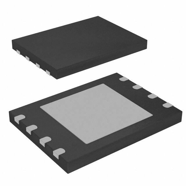


 工商网监
湘ICP备2023018690号
工商网监
湘ICP备2023018690号
