DS1809
Dallastat
FEATURES
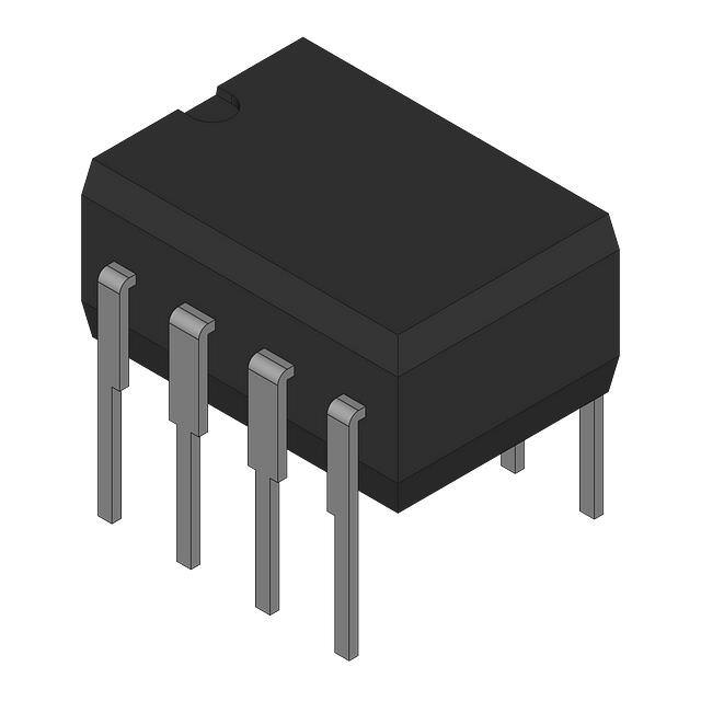
PIN ASSIGNMENT
64-Position Linear Taper
Two Nonvolatile Wiper Storage Options
Operates from +4.5V to +5.5V Supplies
Operating Temperature Range:
- Industrial: -40°C to +85°C
Electronic Interface Provides Either Digital
or Pushbutton Control
Low-Cost Alternative to Mechanical
Solutions
Standard Resistance Values
- DS1809-010
10kΩ
- DS1809-050
50kΩ
- DS1809-100
100kΩ
RH
1
8
VCC
UC
2
7
DC
STR
3
6
RW
RL
4
5
GND
PDIP (300 mils)
SO (150 mils)
μSOP (118 mils)
PIN DESCRIPTION
VCC
RH
RL
RW
UC
DC
STR
GND
-
Supply Voltage
High End of Resistor
Low End of Resistor
Wiper Terminal
Up Control Input
Down Control Input
Storage Enable Input
Ground
DESCRIPTION
The DS1809 Dallastat is a nonvolatile digitally controlled potentiometer that provides 64 uniform wiper
positions over the entire resistor range; including the high-end and low-end terminals of the device. The
DS1809 is a low-power device capable of operating from power supplies of +4.5V to +5.5V. The device
is ideal for low-power, portable, or battery powered applications.
Wiper position is maintained in the absence of power. This is accomplished via the use of an EEPROM
cell array. The device provides for two storage methods, which include an autostore capability and a
command-initiated storage function. The EEPROM cell array is specified to accept greater than 50k
writes. Storage of the wiper position is discussed in the Wiper Storage section of this data sheet.
Wiper positioning is controlled via a dual pushbutton (or contact closure) interface. For simple
pushbutton-controlled applications or CPU-generated control signals, external debounce circuitry is not
needed. The control interface will support both repetitive pulse inputs and continuous pulse (“push-andhold”) inputs. Repetitive pulse and continuous pulse control as well as timing diagrams are discussed in
the Operation.
The DS1809 is available in standard 10 kΩ, 50 kΩ, and 100 kΩ resistor versions. The DS1809 is
provided as an industrial temperature grade part only. Available packaging for the DS1809 include an 8lead (300-mil) PDIP, an 8-lead (150-mil) SO, and an 8-lead (118-mil) µSOP.
1 of 10
19-7387; Rev 4/14
�DS1809
BLOCK DIAGRAM Figure 1
OPERATION
The DS1809 Dallastat is a digitally controlled, nonvolatile potentiometer. A block diagram of the
DS1809 is shown in Figure 1. The DS1809 is a linear potentiometer providing 64-uniform wiper
positions over the entire resistor range including the end-terminals. All three potentiometer terminals of
the device are accessible. These terminals include RH, RL, and RW. RH and RL are the end-terminals of the
potentiometer. These terminals will have a constant resistance between them as defined by the
potentiometer value chosen: 10kΩ, 50kΩ, or the 100kΩ version. Functionally, RH and RL are
interchangeable. The wiper terminal, RW, is the multiplexed terminal and can be set to one of the 64 total
positions that exist on the resistor ladder including the RH and RL terminals.
Control of the wiper (RW) position setting is accomplished via the two inputs UC and DC. The UC and
DC control inputs, when active, determine the direction on the resistor array that the wiper position will
move. The UC (up control) control input is used to move the wiper position towards the RH terminal. The
DC (down control) control input is used to move wiper position towards the RL terminal.
The control inputs UC and DC are active low inputs that interpret input pulse widths as the means of
controlling wiper movement. Internally, these inputs are pulled up to VCC via a 100kΩ resistance. A
transition from a high-to-low on these inputs is considered the beginning of pulse input activity.
A single pulse on the UC or DC input is defined as being greater than 1 millisecond but lasting no longer
that ½ second. This type pulse input will cause the wiper position of the Dallastat to move one position.
Multiple pulse inputs (repetitive pulse inputs) can be used to step through each wiper position of the
device. The requirement for a repetitive pulse train on the UC or DC inputs is that pulses must be
separated by a minimum high time of 1ms. If this is not the case the Dallastat will ignore that pulse input.
A continuous pulse input (“push and hold”) is defined as lasting longer that one-half second. A
continuous pulse input will cause the wiper position to move one position every 100 milliseconds
following the initial one-half-second hold time. The total time to transcend the entire potentiometer given
a continuous pulse input is provided by the equation:
2 of 10
�DS1809
1/2(second) + 62 x 100ms = 6.7 (seconds)
If the wiper position of the DS1809 is incremented to an end-position, it will stay at that position until the
device receives an opposite direction input pulse command over the UC or DC inputs. For example, if the
wiper position is incremented to the RH terminal using the UC input control, it will stay at that position
until UC is first deactivated, and then the DC input is activated to move the wiper position towards the RL
terminal.
The UC and DC control inputs are designed to support simple pushbutton inputs or CPU generated
inputs. Figure 2 illustrates the requirements for pushbutton generated controls. For manual pushbutton
controls, all that is required are the desired pushbuttons to implement contact closure. No external
debounce or timing circuitry is needed to support the pushbutton operation.
Applications using CPU generated controls must power the UC and DC control pins in a high state to
avoid any inadvertent wiper position movement. To help prevent inadvertent wiper position movement
during a power-up, the DS1809 locks out the control port inputs for a minimum time of 10 ms.
WIPER STORAGE
As stated earlier, the DS1809 provides for two methods of nonvolatile wiper storage using internal
EEPROM memory cells. These two methods include an autostore configuration and a command initiated
storage operation, both of which utilize the STR input pin. The EEPROM cell array of the DS1809 is
designed to accept greater than 50k writes.
AUTOSTORAGE
The autostore configuration is designed to provide wiper position storage as the part powers down;
writing the current wiper position into memory. The configuration for initiating the automatic storage
capability of the DS1809 is shown in Figure 3. As shown in this configuration, two external devices are
required to insure proper wiper storage. This includes a Schottky diode and a 10-uf capacitor. The
automatic store configuration will cause the DS1809 to initiate storage of wiper position when power
(VCC) to the device is removed. The 10-uF capacitor and Schottky diode are used to provide supplemental
power for wiper storage.
COMMAND-INITIATED WIPER STORAGE
The DS1809 will also support a command-initiated wiper storage operation during powered conditions.
For command initiated storage the STR pin should be held in a low state on power-up; otherwise the part
will assume an autostore configuration. As shown in Figure 5, a low-to-high pulse lasting at least 1 µs on
the STR input will cause the DS1809 to initiate the storage of the current wiper position into EEPROM
when VCC is present.
3 of 10
�DS1809
PUSHBUTTON CONFIGURATION Figure 2
It is assumed that the STR input will be controlled by either external logic or CPU driven. No external
capacitors or diodes are needed for the command-initiated storage operation.
The STR input will take precedence over the pushbutton inputs UC and DC.
AUTOSTORE CONFIGURATION Figure 3
4 of 10
�DS1809
PUSHBUTTON TIMING DIAGRAMS Figure 4
If during any pushbutton activity the STR input is activated, pushbutton operation will be suspended until
the storage of EEPROM has been completed. Once complete, pushbutton inputs, if still active, will
resume from the point of suspension. Command initiated storage operations will require a minimum of
4 ms to complete the storage operation. This 4ms is measured from the rise of STR input (see Figure 5).
For applications not requiring or using the nonvolatile memory feature of the DS1809, it is recommended
that the STR input be connected to GND.
COMMAND INITIATED WIPER STORAGE - Figure 5
5 of 10
�DS1809
ABSOLUTE MAXIMUM RATINGS
Voltage Range on Any Pin Relative to Ground
Operating Temperature Range
Storage Temperature Range
Soldering Temperature
-1.0V to +7.0V
-40°C to +85°C; industrial
-55°C to +125°C
See J-STD-020A Specification
This is a stress rating only and functional operation of the device at these or any other conditions above those indicated in the operation
sections of this specification is not implied. Exposure to absolute maximum rating conditions for extended periods of time may affect
reliability.
RECOMMENDED DC OPERATING CONDITIONS
(TA = -40°C to +85°C, unless otherwise noted.)
PARAMETER
SYMBOL
MIN
Supply Voltage
VCC
Resistor Inputs
GND
TYP
MAX
UNITS
NOTES
+4.5
5.5
V
1
RL,RH,RW
GND-0.5
VCC+0.5
V
2
GND
GND
GND
1
DC ELECTRICAL CONDITIONS
(TA = -40°C to +85°C, unless otherwise noted.)
PARAMETER
Supply Current Active
SYMBOL
MIN
ICC
TYP
MAX
UNITS
NOTES
500
1000
μA
5
25
μA
6
Standby Current
ISTBY
Logic Input High
VIH
+2.0
VCC+0.5
V
6,11
Logic Input Low
VIL
-0.5
+0.8
+0.6
V
6,11
Input Leakage
IIL
-1
+1
μA
3
RWIPER
400
Ω
Wiper Current
IW
1
mA
Storage Pin Current (STR)
ISP
8
μA
12,18
ms
19
Wiper resistance
Wiper Storage Time
tWST
5
4
6 of 10
�DS1809
AC ELECTRICAL CONDITIONS
PARAMETER
SYMBOL
MIN
Single Input Pulse Width
tPW
Repetitive Pulse High Time
TYP
MAX
UNITS
NOTES
1
DC
ms
4,5,7,9
tHPW
1
DC
ms
4,5,7,8,9
Continuous Pulse
tCCP
1
DC
ms
4,5,7,8,9
Storage Control Pulse
tSTR
1
μs
10,12
Capacitance
CIN
pF
10
5
10
ANALOG RESISTOR CHARACTERISTICS ELECTRICAL CONDITIONS
PARAMETER
SYMBOL
MIN
TYP
MAX
UNITS
NOTES
End-to-End Resistor
Tolerance
-20
+20
%
14
Absolute Linearity
-0.6
+0.6
LSB
15
Relative Linearity
-0.25
+0.25
LSB
16
MHz
17
ppm/ºC
14
-3 dB Cutoff Frequency
fCUTOFF
Temperature Coefficient
750
NOTES:
1. All voltages are referenced with respect to ground.
2. Voltages across the potentiometer terminals (RL, RW, RH) cannot exceed VCC or go below ground by
0.5V.
3. Inputs UC and DC are internally pulled up with resistance of 100kΩ.
4. UC and DC inputs are internally pulled up to VCC via a 100kΩ resistor.
5. Active current is specified when the inputs UC or DC are active.
6. Standby current is the current consumed when the UC, DC, and STR inputs are inactive.
7. Input pulse width is the minimum time required for an input to cause an increment or decrement.
8. Repetitive pulse inputs on UC or DC will be recognized as long as they are within 500ms of each
other. Pulses occurring faster than 1 ms apart may not be recognized as individual and separate
pulses.
9. Input pulse timing has tolerances to ±10%.
10. Capacitance values apply at 25°C.
11. For VCC = 5V±10%, maximum VIL = +0.8V. Input logic levels are referenced to ground.
12. If not used STR should be connected to ground.
13. The DS1809 is offered in three values: 10kΩ, 50kΩ, and 100kΩ.
7 of 10
�DS1809
14. Valid at +25°C only.
15. Absolute linearity is used to compare measured wiper voltage versus expected wiper voltage as
determined by wiper position. The DS1809 is specified to provide a absolute linearity of ±0.60 LSB.
16. Relative linearity is used to determine the change in voltage between successive tap positions. The
DS1809 is specified to provide a relative linearity specification of ±0.25 LSB.
17. -3 dB cutoff frequency characteristics for the DS1809 depend on the potentiometer’s total resistance.
DS1809-010: 1MHz; DS1809-050: 200kHz; and the DS1809-100: 100kHz.
18. Current leakage on the input control storage pin will require a typical 5µA and maximum 8µA to
implement the auto-storage feature.
19. A minimum time of 4ms between 2.2V and 1.7V is required on the input to the STR terminal when
using the part in the auto-storage configuration. The 2.2V to 1.7V range is a worst case condition for
meeting the power-down storage requirements of the part.
8 of 10
�DS1809
ORDERING INFORMATION
PART
DS1809-010+
DS1809-050+
DS1809-100+
DS1809U-010+T
DS1809U-050+T
DS1809U-100+T
DS1809Z-010+
DS1809Z-050+
DS1809Z-100+
TEMP RANGE
-40°C to +85°C
-40°C to +85°C
-40°C to +85°C
-40°C to +85°C
-40°C to +85°C
-40°C to +85°C
-40°C to +85°C
-40°C to +85°C
-40°C to +85°C
VERSION
(kΩ)
10
50
100
10
50
100
10
50
100
PIN-PACKAGE
TOP MARK
8 PDIP
8 PDIP
8 PDIP
8 µSOP
8 µSOP
8 µSOP
8 SO
8 SO
8 SO
DS1809-010
DS1809-050
DS1809-100
1809 X
1809 L
1809 C
DS1809 X
DS1809 L
DS1809 C
+Denotes a lead(Pb)-free/RoHS-compliant package.
T = Tape and reel
PACKAGE INFORMATION
For
the
latest
package
outline
information
and
land
patterns
(footprints),
go
to
www.maximintegrated.com/packages. Note that a “+”, “#”, or “-” in the package code indicates RoHS status
only. Package drawings may show a different suffix character, but the drawing pertains to the package regardless
of RoHS status.
PACKAGE TYPE
PACKAGE CODE
OUTLINE NO.
LAND PATTERN NO.
PDIP
µSOP
SO
P8+1
U8+1
S8+5
21-0043
21-0036
21-0041
—
90-0092
90-0096
9 of 10
�DS1809
REVISION HISTORY
REVISION
DATE
4/14
DESCRIPTION
Added lead(Pb)-free parts and top mark information to the Ordering
Information table; added the Package Information table
PAGES
CHANGED
9
.
10 of 10
Maxim Integrated cannot assume responsibility for use of any circuitry other than circuitry entirely embodied in a Maxim Integrated product. No circuit patent licenses
are implied. Maxim Integrated reserves the right to change the circuitry and specifications without notice at any time. The parametric values (min and max limits)
shown in the Electrical Characteristics table are guaranteed. Other parametric values quoted in this data sheet are provided for guidance.
Maxim Integrated 160 Rio Robles, San Jose, CA 95134 USA 1-408-601-1000
© 2014 Maxim Integrated Products, Inc.
Maxim Integrated and the Maxim Integrated logo are trademarks of Maxim Integrated Products, Inc.
�


 工商网监
湘ICP备2023018690号
工商网监
湘ICP备2023018690号
