19-4859; Rev 8/09
DS80C310
High-Speed Microcontroller
www.maxim-ic.com
GENERAL DESCRIPTION
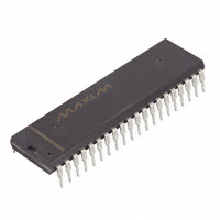
PIN CONFIGURATIONS
The DS80C310 is a fast 80C31/80C32-compatible
microcontroller. It features a redesigned processor
core without wasted clock and memory cycles. As a
result, it executes every 8051 instruction between 1.5x
and 3x faster than the original architecture for the
same crystal speed. Typical applications have a speed
improvement of 2.5x using the same code and the
same crystal. The DS80C310 offers a 25MHz
maximum crystal speed, resulting in apparent
execution speeds of 62.5MHz (approximately 2.5x).
TOP VIEW
The DS80C310 is pin compatible with the standard
80C32 and includes standard resources such as three
timer/counters, 256 bytes of RAM, and a serial port. It
also provides dual data pointers (DPTRs) to speed
block data memory moves. It also can adjust the speed
of MOVX data memory access between two and nine
machine cycles for flexibility in selecting external
memory and peripherals. The DS80C310 offers
upward compatibility with the DS80C320.
FEATURES
80C32 Compatible
8051 Pin and Instruction Set Compatible
Full-Duplex Serial Port
Three 16-Bit Timer/Counters
256 Bytes Scratchpad RAM
Multiplexed Address/Data Bus
Addresses 64kB ROM and 64kB RAM
High-Speed Architecture
4 Clocks/Machine Cycle (8051 = 12)
Runs DC to 25MHz Clock Rates
Single-Cycle Instruction in 160ns
Dual Data Pointer
Optional Variable Length MOVX to Access
Fast/Slow RAM /Peripherals
10 Total Interrupt Sources with 6 External
Internal Power-On Reset Circuit
Upwardly Compatible with the DS80C320
Available in 40-Pin Plastic DIP, 44-Pin PLCC,
and 44-Pin TQFP
Note: Designers must have two documents to fully use all the features
of this device: this data sheet and the High-Speed Microcontroller
User’s Guide, available on our website at www.maximic.com/microcontrollers. Data sheets contain pin descriptions,
feature overviews, and electrical specifications, whereas the user’s
guide contains detailed information about device features and
operation.
Note: Some revisions of this device may incorporate deviations from published specifications known as errata. Multiple revisions of any device
may be simultaneously available through various sales channels. For information about device errata, click here: www.maxim-ic.com/errata.
1 of 22
�DS80C310
ORDERING INFORMATION
PART
DS80C310-MCG
DS80C310-MCG+
DS80C310-QCG
DS80C310-QCG+
DS80C310-QNG
DS80C310-QNG+
DS80C310-ECG
DS80C310-ECG+
MAX CLOCK
SPEED (MHz)
25
25
25
25
25
25
25
25
TEMP RANGE
0C to +70C
0C to +70C
0C to +70C
0C to +70C
-40C to +85C
-40C to +85C
0C to +70C
0C to +70C
+ Denotes a lead(Pb)-free/RoHS-compliant device.
Figure 1. Block Diagram
DS80C310
2 of 22
PIN-PACKAGE
40 Plastic DIP
40 Plastic DIP
44 PLCC
44 PLCC
44 PLCC
44 PLCC
44 TQFP
44 TQFP
�DS80C310
PIN DESCRIPTION
PDIP
PIN
PLCC
TQFP
NAME
FUNCTION
Port 1 (I/O). Port 1 functions as both an 8-bit bidirectional I/O port
and an alternate functional interface for Timer 2 I/O and new
external interrupts. The reset condition of Port 1 is with all bits at
logic 1. In this state, a weak pullup holds the port high. This
condition also serves as an input mode, since any external circuit
that writes to the port overcomes the weak pullup. When software
writes a 0 to any port pin, the DS80C310 activates a strong pulldown
that remains on until either a 1 is written or a reset occurs. Writing a
1 after the port has been at 0 causes a strong transition driver to turn
on, followed by a weaker sustaining pullup. Once the momentary
strong driver turns off, the port once again becomes the output high
(and input) state. The alternate modes of Port 1 are outlined as
follows:
PIN
PORT ALTERNATE
FUNCTION
PDIP PLCC TQFP
1–8
2–9
40–44,
1, 2, 3
P1.0–P1.7
9
10
4
RST
External I/O for
Timer/Counter 2
Timer/Counter 2
Capture/Reload
2
3
41
P1.1
T2EX
Trigger
DS80C320 has a serial
3
4
42
P1.2
—
port RXD
DS80C320 has a serial
4
5
43
P1.3
—
port TXD
External Interrupt 2
5
6
44
P1.4
INT2
(Positive Edge Detect)
External Interrupt 3
6
7
1
P1.5
(Negative Edge
INT3
Detect)
External Interrupt 4
7
8
2
P1.6
INT4
(Positive Edge Detect)
External Interrupt 5
8
9
3
P1.7
(Negative Edge
INT5
Detect)
Reset (Input). The RST input pin contains a Schmitt voltage input to
recognize external active-high reset inputs. The pin also employs an
internal pulldown resistor to allow for a combination of wired-OR
external reset sources.
1
2
3 of 22
40
P1.0
T2
�DS80C310
PDIP
PIN
PLCC
TQFP
NAME
FUNCTION
Port 3 (I/O). Port 3 functions as both an 8-bit bidirectional I/O port
and an alternate functional interface for external Interrupts, Serial
Port 0, Timer 0 and 1 Inputs, RD and WR strobes. The reset
condition of Port 3 is with all bits at logic 1. In this state, a weak
pullup holds the port high. This condition also serves as an input
mode, since any external circuit that writes to the port will overcome
the weak pullup. When software writes a 0 to any port pin, the
DS80C310 will activate a strong pulldown that remains on until
either a 1 is written or a reset occurs. Writing a 1 after the port has
been at 0 will cause a strong transition driver to turn on, followed by
a weaker sustaining pullup. Once the momentary strong driver turns
off, the port once again becomes both the output high and input
state. The alternate modes of Port 3 are as follows:
PDIP
10–17
11,
13–19
5, 7–13
P3.0–P3.7
18, 19
20, 21
14, 15
XTAL2,
XTAL1
21
22
23
24
25
26
27
1, 22,
23
24
25
26
27
28
29
30
16, 17,
39
18
19
20
21
22
23
24
A8 (P2.0)
A9 (P2.1)
A10 (P2.2)
A11 (P2.3)
A12 (P2.4)
A13 (P2.5)
A14 (P2.6)
28
31
25
A15 (P2.7)
20
GND
PIN
PLCC
TQFP
PORT
ALTERNATE
FUNCTION
Serial Port 0
Input
Serial Port 0
11
13
7
P3.1
TXD0
Output
External Interrupt
INT0
12
14
8
P3.2
0
External Interrupt
INT1
13
15
9
P3.3
1
Timer 0 External
14
16
10
P3.4
T0
Input
Timer 1 External
15
17
11
P3.5
T1
Input
External Data
WR
Memory Write
16
18
12
P3.6
Strobe
External Data
RD
17
19
13
P3.7
Memory Read
Strobe
Crystal Oscillator Pins. XTAL1 and XTAL2 provide support for
parallel resonant, AT-cut crystals. XTAL1 also acts as an input in
the event that an external clock source is used in place of a crystal.
XTAL2 serves as the output of the crystal amplifier.
10
11
5
P3.0
RXD0
Digital Circuit Ground
Address Outputs (Port 2) (Output). Port 2 serves as the MSB for
external addressing. P2.7 is A15 and P2.0 is A8. The DS80C310
automatically places the MSB of an address on P2 for external ROM
and RAM access. Although Port 2 can be accessed like an ordinary
I/O port, the value stored on the Port 2 latch is never seen on the pins
(due to memory access). Therefore, writing to Port 2 in software is
only useful for the instructions MOVX A, @ Ri or MOVX @ Ri, A.
These instructions use the Port 2 internal latch to supply the external
address MSB; the Port 2 latch value is supplied as the address
information.
4 of 22
�DS80C310
PDIP
PIN
PLCC
TQFP
NAME
29
32
26
PSEN
30
33
27
ALE
31
35
29
EA
32
33
34
35
36
37
38
39
40
36
37
38
39
40
41
42
43
44
30
31
32
33
34
35
36
37
38
AD7 (P0.7)
AD6 (P0.6)
AD5 (P0.5)
AD4 (P0.4)
AD3 (P0.3)
AD2 (P0.2)
AD1 (P0.1)
AD0 (P0.0)
VCC
–
12, 34
6, 28
N.C.
FUNCTION
Active-Low Program Store Enable (Output). This signal is
commonly connected to external ROM memory as a chip enable.
PSEN is driven high when data memory (RAM) is being accessed
through the bus and during a reset condition.
Address Latch Enable (Output). The output functions as clock to
latch the external address LSB from the multiplexed address/data
bus on Port 0. This signal is commonly connected to the latch enable
of an external 373 family transparent latch. ALE is forced high when
the DS80C310 is in a reset condition.
Active-Low External Access (Input). This pin must be connected to
ground for proper operation.
Address/Data Bus 0–7 (Port 0) (I/O). Port 0 is the multiplexed
address/data bus. During the time when ALE is high, the LSB of a
memory address is presented. When ALE falls to logic 0, the port
transitions to a bidirectional data bus. This bus is used to read
external ROM and read/write external RAM memory or peripherals.
Port 0 has no true port latch and cannot be written directly by
software. The reset condition of Port 0 is high.
+5V Power Supply
No Connection (Reserved). These pins should not be connected.
They are reserved for use with future devices in this family.
COMPATIBILITY
The DS80C310 is a fully static, CMOS, 8051-compatible microcontroller designed for high performance.
In most cases the DS80C310 can drop into an existing socket for the 80C31 or 80C32 to significantly
improve the operation. In general, software written for existing 8051-based systems works without
modification on the DS80C310. The exception is critical timing because the high-speed microcontroller
performs its instructions much faster than the original for any given crystal selection. The DS80C310 runs
the standard 8051 family instruction set and is pin compatible with DIP, PLCC, or TQFP packages. The
DS80C310 is a streamlined version of the DS80C320. It maintains upward compatibility but has fewer
peripherals.
The DS80C310 provides three 16-bit timer/counters, a full-duplex serial port, and 256 bytes of direct
RAM. I/O ports have the same operation as a standard 8051 product. Timers default to a 12 clock-percycle operation to keep their timing compatible with original 8051 family systems. However, timers are
individually programmable to run at the new 4 clocks per cycle if desired.
The DS80C310 provides several new hardware functions that are controlled by Special Function
Registers (SFRs). Table 1 summarizes the SFRs.
PERFORMANCE OVERVIEW
The DS80C310 features a high-speed 8051-compatible core. Higher speed comes not just from increasing
the clock frequency but from a newer, more efficient design.
This updated core does not have the dummy memory cycles that exist in a standard 8051. A conventional
8051 generates machine cycles using the clock frequency divided by 12. In the DS80C310, the same
5 of 22
�DS80C310
machine cycle takes 4 clocks. Thus the fastest instruction, 1 machine cycle, executes three times faster for
the same crystal frequency. Note that these are identical instructions. The majority of instructions on the
DS80C310 will see the full 3-to-1 speed improvement. Some instructions will get between 1.5 and 2.4 to
1 improvement. All instructions are faster than the original 8051.
The numerical average of all op codes gives approximately a 2.5-to-1 speed improvement. Improvement
of individual programs depends on the actual instructions used. Speed-sensitive applications would make
the most use of instructions that are three times faster. However, the sheer number of 3-to-1 improved
op codes makes dramatic speed improvements likely for any code. These architecture improvements and
0.8m CMOS produce a peak instruction cycle in 160ns (6.25MIPS). The dual data pointer feature also
allows the user to eliminate wasted instructions when moving blocks of memory.
INSTRUCTION SET SUMMARY
All instructions in the DS80C310 perform the same functions as their 8051 counterparts. Their effect on
bits, flags, and other status functions is identical. However, the timing of each instruction is different.
This applies both in absolute and relative number of clocks.
For absolute timing of real-time events, the timing of software loops can be calculated using a table in the
High-Speed Microcontroller User’s Guide. However, counter/timers default to run at the older 12 clocks
per increment. In this way, timer-based events occur at the standard intervals with software executing at
higher speed. Timers optionally can run at 4 clocks per increment to take advantage of faster processor
operation.
The relative time of two instructions might be different in the new architecture than it was previously. For
example, in the original architecture the “MOVX A, @ DPTR” instruction and the “MOV direct, direct”
instruction used 2 machine cycles or 24 oscillator cycles. Therefore, they required the same amount of
time. In the DS80C310, the MOVX instruction takes as little as 2 machine cycles or 8 oscillator cycles
but the “MOV direct, direct” uses 3 machine cycles or 12 oscillator cycles. While both are faster than
their original counterparts, they now have different execution times. This is because the DS80C310
usually uses 1 instruction cycle for each instruction byte. The user concerned with precise program timing
should examine the timing of each instruction for familiarity with the changes. Note that a machine cycle
now requires just 4 clocks, and provides one ALE pulse per cycle. Many instructions require only 1 cycle,
but some require 5. In the original architecture, all were 1 or 2 cycles except for MUL and DIV. Refer to
the High-Speed Microcontroller User’s Guide for details and individual instruction timing.
6 of 22
�DS80C310
SPECIAL FUNCTION REGISTERS (SFRs)
Special Function Registers control most special features of the DS80C310. The High-Speed
Microcontroller User’s Guide contains descriptions of all the SFRs. Functions that are not part of the
standard 80C32 are in bold.
Table 1. Special Function Registers
REGISTER
SP
DPL
DPH
DPL1
DPH1
DPS
PCON
TCON
TMOD
TL0
TL1
TH0
TH1
CKCON
P1
EXIF
SCON
SBUF
P2
IE
SADDR0
P3
IP
SADEN0
STATUS
T2CON
T2MOD
RCAP2L
RCAP2H
TL2
TH2
PSW
WDCON
ACC
EIE
B
EIP
BIT 7
—
—
—
—
—
0
SMOD
TF1
GATE
—
—
—
—
—
P1.7
IE5
SMO/FE
—
P2.7
EA
—
P3.7
—
—
0
TF2
—
—
—
—
—
CY
—
—
—
—
—
BIT 6
—
—
—
—
—
0
SM0D0
TR1
C/ T
—
—
—
—
—
P1.6
IE4
SM1
—
P2.6
—
—
P3.6
—
—
HIP
EXF2
—
—
—
—
—
AC
POR
—
—
—
—
BIT 5
—
—
—
—
—
0
—
TF0
M1
—
—
—
—
T2M
P1.5
IE3
SM2
—
P2.5
ET2
—
P3.5
PT2
—
LIP
RCLK
—
—
—
—
—
F0
—
—
—
—
—
BIT 4
—
—
—
—
—
0
—
TR0
M0
—
—
—
—
T1M
P1.4
IE2
REN
—
P2.4
ES0
—
P3.4
PSO
—
1
TCLK
—
—
—
—
—
RS1
—
—
—
—
—
7 of 22
BIT 3
—
—
—
—
—
0
GF1
IE1
GATE
—
—
—
—
T0M
P1.3
—
TB8
—
P2.3
ET1
—
P3.3
PT1
—
1
EXEN2
—
—
—
—
—
RS0
—
—
EX5
—
PX5
BIT 2
—
—
—
—
—
0
GF0
IT1
C/ T
—
—
—
—
MD2
P1.2
—
RB8
—
P2.2
EX1
—
P3.2
PX1
—
1
TR2
—
—
—
—
—
OV
—
—
EX4
—
PX4
BIT 1
—
—
—
—
—
0
STOP
IE0
M1
—
—
—
—
MD1
P1.1
—
TI
—
P2.1
ET0
—
P3.1
PT0
—
1
BIT 0
—
—
—
—
—
SEL
IDLE
IT0
M0
—
—
—
—
MD0
P1.0
—
RI
—
P2.0
EX0
—
P3.0
PX0
—
1
C/ T2
T2OE
—
—
—
—
FL
—
—
EX3
—
PX3
CP/ RL2
DCEN
—
—
—
—
P
—
—
EX2
—
PX2
ADDRESS
81h
82h
83h
84h
85h
86h
87h
88h
89h
8Ah
8Bh
8Ch
8Dh
8Eh
90h
91h
98h
99h
A0h
A8h
A9h
B0h
B8h
B9h
C5h
C8h
C9h
CAh
CBh
CCh
CDh
D0h
D8h
E0h
E8h
F0h
F8h
�DS80C310
MEMORY ACCESS
The DS80C310 has 256 bytes of scratchpad RAM, but contains no on-chip ROM. Off-chip memory is
accessed using the multiplexed address/data bus on P0 and the MSB address on P2. Timing diagrams are
provided in the Absolute Maximum Ratings section. Program memory (ROM) is accessed at a fixed rate
determined by the crystal frequency and the actual instructions. As mentioned above, an instruction cycle
requires 4 clocks. Data memory (RAM) is accessed according to a variable speed MOVX instruction as
described below.
STRETCH MEMORY CYCLE
The DS80C310 allows the application software to adjust the speed of data memory access. The
microcontroller can perform the MOVX in as few as 2 instruction cycles. However, this value can be
stretched as needed so that both fast memory and slow memory or peripherals can be accessed with no
glue logic. Even in high-speed systems, it may not be necessary or desirable to perform data memory
access at full speed. In addition, there are a variety of memory-mapped peripherals such as LCD displays
or UARTs that are not fast.
The stretch MOVX is controlled by the Clock Control Register at SFR location 8Eh as described below.
This allows the user to select a stretch value between 0 and 7. A stretch of 0 results in a 2-machine-cycle
MOVX. A stretch of 7 results in a MOVX of 9 machine cycles. Software can dynamically change this
value depending on the particular memory or peripheral.
On reset, the stretch value defaults to 1, resulting in a 3-cycle MOVX. Therefore, RAM access is not
performed at full speed. This is a convenience to existing designs that may not have fast RAM in place.
When maximum speed is desired, the software should select a stretch value of 0. When using very slow
RAM or peripherals, a larger stretch value can be selected. Note that this affects data memory only and
the only way to slow program memory (ROM) access is to use a slower crystal.
Using a stretch value between 1 and 7 causes the microcontroller to stretch the read/write strobe and all
related timing. This results in a wider read/write strobe allowing more time for memory/peripherals to
respond. The timing of the variable speed MOVX is shown in the Absolute Maximum Ratings section.
Note that full speed access is not the reset default case. Table 2 shows the resulting strobe widths for each
stretch value. The memory stretch is implemented using the Clock Control Special Function Register at
SFR location 8Eh. The stretch value is selected using bits CKCON.2–CKCON.0. In the table, these bits
are referred to as M2 through M0. The first stretch (default) allows the use of common 120ns or 150ns
RAMs without dramatically lengthening the memory access.
8 of 22
�DS80C310
Table 2. Data Memory Cycle Stretch Values
CKCON.2–CKCON.0
M2
0
0
0
0
1
1
1
1
M1
0
0
1
1
0
0
1
1
M0
0
1
0
1
0
1
0
1
MEMORY
CYCLES
RD OR WR STROBE
WIDTH IN CLOCKS
25MHz STROBE WIDTH
(ns)
2
3 (default)
4
5
6
7
8
9
2
4
8
12
16
20
24
28
80
160
320
480
640
800
960
1120
DUAL DATA POINTER (DPTR)
Data memory block moves can be accelerated using the DS80C310 dual data pointer (DPTR). The
standard 8032 DPTR is a 16-bit value that is used to address off-chip data RAM or peripherals. In the
DS80C310, the standard data pointer is called DPTR and is located at SFR addresses 82h and 83h. These
are the standard locations. No modification of standard code is needed to use DPTR. The new DPTR is
located at SFR 84h and 85h and is called DPTR1. The DPTR select bit (DPS) chooses the active pointer
and is located at the LSB of the SFR location 86h. No other bits in register 86h have any effect and are set
to 0. The user switches between data pointers by toggling the LSB of register 86h. The increment (INC)
instruction is the fastest way to accomplish this. All DPTR-related instructions use the currently selected
DPTR for any activity. Therefore, only one instruction is required to switch from a source to a destination
address. Using the DPTR saves code from needing to save source and destination addresses when doing a
block move. Once loaded, the software simply switches between DPTR0 and 1. The relevant register
locations are as follows.
DPL
DPH
DPL1
DPH1
DPS
82h
83h
84h
85h
86h
Low byte original DPTR
High byte original DPTR
Low byte new DPTR
High byte new DPTR
DPTR Select (lsb)
STOP MODE ENHANCEMENTS
Setting bit 1 of the Power Control Register (PCON; 87h) invokes the stop mode. Stop mode is the lowest
power state because it turns off all internal clocking. The ICC of a standard stop mode is approximately
1A (but is specified in the Absolute Maximum Ratings section). The CPU exits stop mode from an
external interrupt or a reset condition. Internally generated interrupts are not useful since they require
clocking activity.
The DS80C310 allows a resume from stop using INT2–INT5, which are edge-triggered interrupts. An
internal crystal counter manages the startup timing. A delay of 65,536 clocks occurs to allow the crystal
time to stabilize. Software must also insert a delay of 100 machine cycles following the exit from stop
mode. This ensures stabilization of internal timing prior to time-critical software tasks such as serial port
operations or bus access to memory-mapped I/O devices.
9 of 22
�DS80C310
PERIPHERAL OVERVIEW
The DS80C310 provides the same peripheral functions as the standard 80C32. The device is compatible
with the DS80C320, but it does not offer all the peripherals.
TIMER RATE CONTROL
There is one important difference between the DS80C310 and 8051 regarding timers. The original 8051
used 12 clocks per cycle for timers and machine cycles. The DS80C310 architecture normally uses 4
clocks per machine cycle. However, in the area of timers and serial ports, the DS80C310 defaults to 12
clocks per cycle on reset. This allows existing code with real-time dependencies such as baud rates to
operate properly.
If an application needs higher speed timers or serial baud rates, the user can select individual timers to run
at the 4-clock rate. The Clock Control Register (CKCON; 8Eh) determines these timer speeds. When the
relevant CKCON bit is logic 1, the DS80C310 uses 4 clocks per cycle to generate timer speeds. When the
bit is 0, the DS80C310 uses 12 clocks for timer speeds. The reset condition is 0. CKCON.5 selects the
speed of Timer 2. CKCON.4 selects Timer 1 and CKCON.3 selects Timer 0. Note that unless a user
desires very fast timing, it is unnecessary to alter these bits. Also note that the timer controls are
independent.
POWER-ON RESET
The DS80C310 holds itself in reset during a power-up until 65,536 clock cycles have elapsed. The poweron reset used by the DS80C310 differs somewhat from other members of the high-speed microcontroller
family. The crystal oscillator can start anywhere between 1.0V and 4.5V, but is not specified. This
eliminates the need for an RC reset circuit. For voltage-specific precision-brownout detection, an external
component is needed. When the device goes through a power-on reset, the POR flag is set in the
WDCON (D8h) register at bit 6.
INTERRUPTS
The DS80C310 provides 10 interrupt sources with two priority levels. Software can assign high or low
priority to all sources. All interrupts that are new to the 8051 have a lower natural priority than the
originals.
Table 3. Interrupt Sources and Priorities
NAME
DESCRIPTION
VECTOR
INT0
TF0
INT1
TF1
SCON
TF2
INT2
INT3
INT4
INT5
External Interrupt 0
Timer 0
External Interrupt 1
Timer 1
T1 or R1 from the serial port
Timer 2
External Interrupt 2
External Interrupt 3
External Interrupt 4
External Interrupt 5
03h
0Bh
13h
1Bh
23h
2Bh
43h
4Bh
53h
5Bh
10 of 22
NATURAL
PRIORITY
1
2
3
4
5
6
7
8
9
10
�DS80C310
ABSOLUTE MAXIMUM RATINGS
Voltage Range on Any Pin Relative to Ground……………………………………...-0.3V to (VCC + 0.5V)
Voltage Range on VCC Relative to Ground………………………………………………….-0.3V to +6.0V
Operating Temperature Range………………………………………………………………-40C to +85C
Storage Temperature Range……………………………………………………………….-55C to +125C
Soldering Temperature………………………………………….See IPC/JEDEC J-STD-020 Specification
This is a stress rating only and functional operation of the device at these or any other conditions above those indicated in the
operation sections of this specification is not implied. Exposure to absolute maximum rating conditions for extended periods of
time may affect device reliability.
DC ELECTRICAL CHARACTERISTICS
(VCC = 4.5V to 5.5V, TA = -40C to +85C.) (Note 1)
PARAMETER
SYMBOL
Supply Voltage
VCC
Supply Current Active Mode
ICC
at 25MHz
Supply Current Idle Mode
IIDLE
at 25MHz
Supply Current Stop Mode
ISTOP
Input Low Level
VIL
Input High Level (Except XTAL1 and
VIH
RST)
Input High Level XTAL1 and RST
Output Low Voltage Ports 1, 3
at IOL = 1.6mA
Output Low Voltage Port 0, 2, ALE,
PSEN at IOL = 3.2mA
Output High Voltage Port 1, 3, ALE,
PSEN at IOH = -50A
Output High Voltage Ports 1, 3
at IOH = -1.5mA
Output High Voltage Port 0, 2, ALE,
PSEN at IOH = -8mA
Input Low Current Ports 1, 3
at 0.45V
Transition Current from 1 to 0
Ports 1, 3 at 2V
Input Leakage Port 0, Bus Mode
RST Pulldown Resistance
Note 1:
Note 2:
Note 3:
Note 4:
Note 5:
VIH2
MIN
4.0
TYP
5.0
MAX
5.5
UNITS
V
NOTES
2
30
mA
3
15
mA
4
A
V
5
2
V
2
V
2
1
-0.3
+0.8
VCC +
0.3
VCC +
0.3
2.0
3.5
VOL1
0.15
0.45
V
2
VOL2
0.15
0.45
V
2, 6
VOH1
2.4
V
2, 7
VOH2
2.4
V
2, 8
VOH3
2.4
V
2, 6
IIL
-55
A
9
ITL
-650
A
10
+300
170
A
k
11
IL
RRST
-300
50
All parameters apply to both commercial and industrial temperature operation unless otherwise noted. Specifications to -40C
are guaranteed by design and not product tested.
All voltages are referenced to ground.
Active current is measured with a 25MHz clock source driving XTAL1, VCC = RST = 5.5V, all other pins disconnected.
Idle mode current is measured with a 25MHz clock source driving XTAL1, VCC = 5.5V, RST at ground, all other pins
disconnected.
Stop mode current measured with XTAL1 and RST grounded, VCC =5.5V, all other pins disconnected.
11 of 22
�DS80C310
Note 6:
Note 7:
Note 8:
Note 9:
Note 10:
Note 11:
When addressing external memory. This specification applies to the first clock cycle following the transition. On subsequent
cycles following 1 to 0 transitions, the typical current sink capability of Port 0 and Port 2 is approximately 150A, and the
minimum current sink capability of ALE and PSEN is approximately 400A. On subsequent cycles following 0 to 1
transitions, the typical current drive capability of Port 0 and Port 2 is approximately 110A.
RST = VCC. This condition mimics operation of pins in I/O mode.
During a 0 to 1 transition, a one-shot drives the ports hard for two clock cycles. This measurement reflects port in transition
mode.
Current required from external circuit to hold a logic-low level on an I/O pin while the corresponding port latch bit is set to 1.
This is only the current required to hold the low level; transitions from 1 to 0 on an I/O pin must also overcome the transition
current.
Ports 1 and 3 source transition current when being pulled down externally. The current reaches its maximum at approximately
2V.
0.45 < VIN 0
tMCS=0
tMCS>0
tMCS=0
tMCS>0
tMCS=0
tMCS>0
tMCS=0
tMCS>0
tMCS=0
tMCS>0
ns
ns
ns
ns
tMCS=0
tMCS>0
tMCS=0
tMCS>0
tMCS=0
tMCS>0
tMCS=0
ns
ns
ns
ns
tMCS>0
tMCS=0
tMCS>0
tMCS=0
tMCS>0
tMCS=0
tMCS>0
ns
ns
tMCS=0
tMCS>0
ns
ns
tMCS=0
tMCS>0
tMCS is a time period related to the stretch memory cycle selection. The following table shows the value of tMCS for each
stretch selection.
M2
0
0
0
0
1
1
1
1
M1
0
0
1
1
0
0
1
1
M0
0
1
0
1
0
1
0
1
MOVX CYCLES
2 machine cycles
3 machine cycles (default)
4 machine cycles
5 machine cycles
6 machine cycles
7 machine cycles
8 machine cycles
9 machine cycles
tMCS
0
4 tCLCL
8 tCLCL
12 tCLCL
16 tCLCL
20 tCLCL
24 tCLCL
28 tCLCL
14 of 22
�DS80C310
Note 2:
Address is held in a weak latch until overdriven by external memory.
EXTERNAL CLOCK CHARACTERISTICS
PARAMETER
Clock High Time
Clock Low Time
Clock Rise Time
Clock Fall Time
SYMBOL
tCHCX
tCLCX
tCLCL
tCHCL
MIN
10
10
TYP
MAX
5
5
UNITS
ns
ns
ns
ns
SERIAL PORT MODE 0 TIMING CHARACTERISTICS
PARAMETER
SYMBOL
Serial Port Clock Cycle
Time
tXLXL
Output Data Setup to
Clock Rising
tQVXH
Output Data Hold from
Clock Rising
tXHQX
Input Data Hold after
Clock Rising
tXHDX
Clock Rising Edge to
Input Data Valid
tXHDV
CONDITIONS
SM2 = 0, 12 clocks per cycle
MIN
TYP
12tCLCL
SM2 = 1, 4 clocks per cycle
4tCLCL
SM2 = 0, 12 clocks per cycle
10tCLCL
SM2 = 1, 4 clocks per cycle
3tCLCL
SM2 = 0, 12 clocks per cycle
2tCLCL
SM2 = 1, 4 clocks per cycle
tCLCL
SM2 = 0, 12 clocks per cycle
tCLCL
MAX
UNITS
ns
ns
ns
ns
SM2 = 1, 4 clocks per cycle
tCLCL
SM2 = 0, 12 clocks per cycle
11tCLCL
SM2 = 1, 4 clocks per cycle
3tCLCL
ns
DEFINITION OF AC SYMBOLS
In an effort to remain compatible with the original 8051 family, this device specifies the same parameters
as such devices, using the same symbols. For completeness, the following are description of the symbols.
t
A
C
D
H
L
I
P
Q
R
V
W
X
Z
Time
Address
Clock
Input Data
Logic Level High
Logic Level Low
Instruction
PSEN
Output Data
RD Signal
Valid
WR Signal
No longer a valid logic level
Tri-State
15 of 22
�DS80C310
EXTERNAL PROGRAM MEMORY READ CYCLE
16 of 22
�DS80C310
EXTERNAL DATA MEMORY READ CYCLE
17 of 22
�DS80C310
DATA MEMORY WRITE CYCLE
DATA MEMORY WRITE WITH STRETCH = 1
18 of 22
�DS80C310
DATA MEMORY WRITE WITH STRETCH = 2
EXTERNAL CLOCK DRIVE
19 of 22
�DS80C310
SERIAL PORT MODE 0 TIMING
20 of 22
�DS80C310
PACKAGE INFORMATION
For the latest package outline information and land patterns, go to www.maxim-ic.com/packages.
PACKAGE TYPE
PACKAGE CODE
DOCUMENT NO.
44 TQFP
40 PDIP
44 PLCC
C44+2
P40+1
Q44+1
21-0293
21-0044
21-0049
21 of 22
�DS80C310
REVISION HISTORY
REVISION
DATE
090198
012401
102405
042106
8/09
DESCRIPTION
1) Added note to clarify IIL specification.
2) Changed serial port mode 0 timing diagram label from tQVXL to
tQVXH .
3) Changed minimum oscillator frequency to 1MHz when using
external crystal.
4) Corrected “Data memory write with stretch” diagrams to show
falling edge of ALE coincident with rising edge of C3 clock.
1) Added errata disclaimer to page 1.
1) Device moved to qualified status. Removed “Preliminary” status
from data sheet.
2) Removed references to 33MHz versions of the device.
3) Added note requiring 100 machine cycles delay following stop
mode exit. This edit transfers existing erratum from errata sheet
into data sheet.
4) Updated Absolute Maximum Ratings table to match current
format.
5) Displayed Electrical Characteristics test conditions.
6) Added notation that -40C specifications are guaranteed by
design but not tested.
7) Clarified DC Electrical Characteristics note that the specification
only applies to the first clock cycle following the transition.
8) Added lead-free part numbers to Ordering Information table.
9) Added tAVLL2 specification.
10) Updated AC timing characteristics with full characterization
data.
1) Changed lead-free ordering information part numbers to
correctly reflect that the “+” comes after part numbers (e.g.,
DS80C310-MCG+).
2) Added Note 2 to the AC Electrical Characteristics and MOVX
Characteristics tables.
Removed additional references to 33MHz versions of the device.
PAGES
CHANGED
13, 14
1, 11
22 of 22
Maxim cannot assume responsibility for use of any circuitry other than circuitry entirely embodied in a Maxim product. No circuit patent licenses are implied. Maxim
reserves the right to change the circuitry and specifications without notice at any time.
Maxim Integrated Products, 120 San Gabriel Drive, Sunnyvale, CA 94086 408-737-7600
© 2009 Maxim Integrated Products
Maxim is a registered trademark of Maxim Integrated Products, Inc.
�


 工商网监
湘ICP备2023018690号
工商网监
湘ICP备2023018690号
