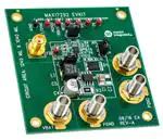
Evaluates: MAX17292
MAX17292 Evaluation Kit
General Description
The MAX17292 evaluation kit (EV kit) is a fully assembled
and tested PCB that contains a 16W DC-DC boost converter
for battery-operated, harsh environment, front-end preboost
applications. The MAX17292 integrates a low-side FET driver
and current-mode, control-loop circuitry for output-voltage
regulation, making it ideal for boost or SEPIC converters.
The MAX17292’s integrated driver switches at 2.2MHz. The
device can be synchronized with an external clock source
within the 1MHz to 2.5MHz range.
The EV kit operates from a DC supply voltage of 3V
up to 8V. The EV kit can withstand a 16V line transient
condition. The EV kit demonstrates the device features,
such as dynamic adjustable output voltage, external
clock synchronization, two-phase operation configurability,
cycle-by-cycle current limit, hiccup mode, and thermal
shutdown. The boost converter regulates 8V and can
supply a current up to 2A. The EV kit also demonstrates
a reference MAX17292 design for battery-operated, harsh
environment applications.
Quick Start
Required Equipment
• MAX17292 EV kit
• 3V to 8V, 10A DC power supply
• Digital voltmeter (DVM)
• 2A load
Output Testing
This EV kit is fully assembled and tested. Follow the steps
below to verify board operation. Caution: Do not turn on
the power supply until all connections are completed.
1) Verify that a shunt is installed on pins 1-2 of jumper
JU1 (device enabled).
2) Verify that a shunt is installed on pins 1-2 (normal
mode) or 2-3 (bootstrapped mode) on jumper JU2.
3) Verify that a shunt is installed on jumper JU3 (internal
1V reference).
Features
4) Connect the power supply’s positive terminal to the
VBAT PCB banana jack and the power supply’s ground
to the PGND PCB banana jack.
●● 87% Peak Efficiency at 5V Input
5) Connect the load across the VOUT and PGND
banana jacks.
●● 8V up to 2A Output
6) Connect the DVM across VOUT and PGND.
●● Demonstrates External Clock Synchronization
7) Turn on the power supply and set it to 4.5V.
●● Spread Spectrum Optimizes EMI Performance
8) Measure VOUT and verify that it is 8V.
●● 3V Up to 8V Input Voltage Range
●● Demonstrates SUP UVLO
●● Demonstrates Cycle-by-Cycle Current Limit and
Hiccup Mode
●● Thermal-Shutdown Protection
●● PGOOD Flag
●● Demonstrates Dynamic Adjustable Output
●● Demonstrates 2.2MHz Single/Two-Phase Operation
●● Compact 1240mil x 1040mil Overall Circuit Footprint
Design (0.775 sq. in.)
●● Proven 4-Layer 2oz. PCB Layout and Thermal Design
●● Fully Assembled and Tested
19-8641; Rev 0; 9/16
Ordering Information appears at end of data sheet.
�Evaluates: MAX17292
MAX17292 Evaluation Kit
Detailed Description of Hardware
Bootstrap Mode
The MAX17292 EV kit is a fully assembled and tested
4-layer PCB that contains a 16W DC-DC boost converter
for battery-operated, harsh environment applications, such
as front-end, preboost power-suppy applications. The EV kit
demonstrates the device’s features, such as the integrated
low-side FET driver and current-mode control-loop circuitry
for output-voltage regulation. The device’s integrated driver
switches at 2.2MHz and can be synchronized with an external
clock source within the 1MHz to 2.5MHz range.
The EV kit operates from a DC supply voltage of 3V up
to 8V. The EV kit can withstand a 16V line transient, that
is limited by input capacitor C4 maximum voltage or U1
specific pin 16V rating, which ever is less. The EV kit
demonstrates the device features such as dynamic adjustable output voltage, external clock synchronization, single/
two-phase operation configurability, cycle-by-cycle current
limit, hiccup mode, and thermal shutdown. The boost
converter regulates 8V and can supply a current up to 2A.
Enable
The EV kit features an enable input and a jumper (JU1)
that can be used to enable/disable the device and place
it in shutdown mode. The EV kit is enabled whenever
power is applied to VBAT and PGND above 4.5V and EN
is pulled high.
To enable the EV kit from an external enable signal,
remove the shunt from JU1 and apply a logic signal on the
EN and AGND test points of the EV kit. The enable (EN)
input should not be left unconnected (see Table 1 below).
Refer to the EN pin description in the MAX17292 IC data
sheet for additional information. See Table 1 for EN settings.
Table 1. Enable (JU1)
For applications where the input voltage goes below 4.5V,
use the device in bootstrapped mode by installing a shunt
on pins 2-3 of jumper JU2. In bootstrapped configuration,
the device is supplied by the output of the boost regulator
itself and does not trigger the UVLO, even if the input
voltage goes down to 3V. See Table 2 for jumper JU2
settings.
Output-Voltage Adjustment
The VOUT output voltage can be dynamically adjusted by
feeding an analog voltage to the REFIN and AGND test
points. The external voltage applied to REFIN is used as
the FB reference. Remove the shunt on JU3 to apply an
external voltage to REFIN. With the shunt installed on
jumper JU3, REFIN is shorted to PVL and an internal 1V
FB reference is used for loop regulation. The output voltage
can be adjusted in the range of 4V to 16V. See Table 3 for
jumper JU3 settings.
External Clock Synchronization
The MAX17292 IC can be synchronized using an external
clock applied to the FSET/SYNC and AGND test points.
A falling clock edge on FSET/SYNC turns on the external
MOSFET by driving DRV high after a short delay. The
MAX17292 can be synchronized with an external clock
source within the 1MHz to 2.5MHz range, and a logic-high
voltage range of 2.5V to 5V.
SHUNT POSITION
EN PIN
Installed*
Connected to VBAT
Enabled
Connected to AGND
Connected to an external controller
Disabled
External controller enabled
SHUNT POSITION
SUP PIN
EV KIT OPERATION
1-2*
Connected to VBAT
Normal
2-3
Connected to VOUT
Bootstrapped
*Default position.
Installed
Removed
EV KIT OPERATION
Table 2. Bootstrap Mode (JU2)
*Default position.
www.maximintegrated.com
Maxim Integrated │ 2
�Evaluates: MAX17292
MAX17292 Evaluation Kit
Two-Phase Configuration
To configure the EV kit for two-phase operation, use two
EV kits and follow the instructions below:
Master EV kit:
1) Install a 0603 surface-mount 1kΩ resistor on the R8 pads.
Slave EV kit:
1) Remove resistors R2 and R1.
2) Remove capacitors C2, C3, and resistor R5.
3) Install a 0603 surface mount 0Ω resistor on R11 pads.
Make the following connections:
1) Connect the PGND banana jack on the master to
PGND banana jack on the slave.
2) Connect the AGND test point on the master to
AGND test point on the slave.
3) Connect the VBAT banana jack on the master to
VBAT banana jack on the slave.
4) Connect the VOUT banana jack on the master to
VOUT banana jack on the slave.
5) Connect the COMP PCB pin on the master to
COMP pin on the slave through a SMA cable.
6) Connect the SYNCO test point on the master to
FSET/SYNC test point on the slave.
the
the
the
the
the
the
Table 3. Output Voltage Adjustment (JU3)
SHUNT POSITION
SUP PIN
EV KIT OPERATION
1-2*
Connected to VBAT
Normal
2-3
Connected to VOUT
Bootstrapped
*Default position.
Component Suppliers
SUPPLIER
WEBSITE
Fairchild Semiconductor
www.fairchildsemi.com
Kemet
www.kemet.com
Murata Americas
www.murata.com
NXP
www.nxp.com
Panasonic Corp.
www.panasonic.com
Wurth Electronik GmbH
www.we-online.com
Note: Indicate that you are using the MAX17292 when contacting these component suppliers.
www.maximintegrated.com
Maxim Integrated │ 3
�Evaluates: MAX17292
MAX17292 Evaluation Kit
MAX17292 EV Bill of Materials
Reference
Designators
Description
Qty
AGND
1
TEST POINT; PIN DIA=0.1IN; TOTAL LENGTH=0.3IN; BOARD HOLE=0.04IN; BLACK; PHOSPHOR
BRONZE WIRE SILVER PLATE FINISH
EN, FB, FSET/
SYNC, PGOOD,
PVL, REFIN,
SYNCO
7
TEST POINT; PIN DIA=0.1IN; TOTAL LENGTH=0.3IN; BOARD HOLE=0.04IN; RED; PHOSPHOR
BRONZE WIRE SILVER PLATE FINISH
C1
1
CAPACITOR; SMT; (1210); CERAMIC CHIP; 47UF; 16V; TOL=10%; MODEL=GRM SERIES; TG=-55
DEGC TO +85 DEGC; TC=X5R
C2
1
CAPACITOR; SMT; (0603); CERAMIC; 6200pF; 50V; ±5%; C0G, NP0; -55degC to + 125degC.
C3
1
CAPACITOR; SMT; (0603); CERAMIC; 150pF; 50V; ±5%; C0G, NP0; -55degC to + 125degC.
C4
1
CAPACITOR; SMT; (SMD); ALUMINUM-ELECTROLYTIC; 47UF; 50V; TOL=20%
C5, C11
2
CAPACITOR; SMT; (0805); CERAMIC CHIP; 1UF; 50V; TOL=10%; TG=-55 DEGC TO +125 DEGC;
TC=X7R
C6
1
CAPACITOR; SMT; (0603); CERAMIC CHIP; 2.2UF; 10V; TOL=10%; TG=-55 DEGC TO +125 DEGC;
TC=X7R;
C12
1
CAPACITOR; SMT; (0402); CERAMIC CHIP; 0.1UF; 16V; TOL=10%; TG=-55 DEGC TO +125 DEGC;
TC=X7R;
COMP
1
CONNECTOR; FEMALE THREADED; THROUGH HOLE; SMA; STRAIGHT THROUGH; 5PINS
D1
1
DIODE; SCH; SMT; (SOT-1289); PIV=45V; IF=15A
JU1, JU2
2
CONNECTOR; MALE; THROUGH HOLE; BREAKAWAY; STRAIGHT; 3PINS
JU3
1
CONNECTOR; MALE; THROUGH HOLE; BREAKAWAY; STRAIGHT; 2PINS
L1
1
0.47uH, 18A inductor (7mm x 6.9mm)
N1
1
TRAN; N-CHANNEL POWERTRENCH MOSFET; NCH; SO-8; PD-(2.5W); I-(10A); V-(60V)
R1
1
RESISTOR; 0402; 90.9 kOHM; 1%; 100PPM; 0.10W; METAL FILM
R2
1
RESISTOR; 0402; 13.0 kOHM; 1%; 100PPM; 0.10W; METAL FILM
R3
1
RESISTOR; 1812; 0.022 OHM; 1%; 300PPM; 0.5W; THICK FILM
R4
1
RESISTOR; 0402; 1 kOHM; 1%
R5
1
RESISTOR; 0402; 6.81 kOHM; 1%
R6
1
RESISTOR; 0402; 10 kOHM; 5%
R7
1
RESISTOR; 0402; 12.1 kOHM; 1%
R9
1
RESISTOR; 0402; 0 OHM; 0%; JUMPER; 0.10W; THICK FILM
PGND (2x),
VOUT, SUP
4
CONNECTOR; MALE; PANELMOUNT; BANANA JACK; STRAIGHT; 1PIN
U1
1
EVKIT PART-IC; MAX17292; PACKAGE OUTLINE: 21-0136; PACKAGE CODE: T1233-4; TQFN12-EP
C7
0
PACKAGE OUTLINE 1210 NON-POLAR CAPACITOR
C8
0
PACKAGE OUTLINE 0402 NON-POLAR CAPACITOR
C9, C10
0
PACKAGE OUTLINE 0603 NON-POLAR CAPACITOR
R8, R11
0
PACKAGE OUTLINE 0402 RESISTOR
R14, R15
0
PACKAGE OUTLINE 0603 RESISTOR
PCB
1
PCB Board:MAX17292 EVALUATION KIT
www.maximintegrated.com
Maxim Integrated │ 4
�MAX17292 Evaluation Kit
Evaluates: MAX17292
MAX17292 EV PCB Layout Diagrams
MAX17292 EV Kit—Top Silkscreen
MAX17292 EV Kit—Component Side
MAX17292 EV Kit—Layer 2 GND
MAX17292 EV Kit—Layer 3
www.maximintegrated.com
Maxim Integrated │ 5
�MAX17292 Evaluation Kit
Evaluates: MAX17292
MAX17292 EV PCB Layout Diagrams (continued)
MAX17292 EV Kit—Solder Side
MAX17292 EV Minimal Component Schematic
www.maximintegrated.com
Maxim Integrated │ 6
�MAX17292 Evaluation Kit
Evaluates: MAX17292
MAX17292 EV Schematic
Ordering Information
PART
MAX17292EVKIT#
TYPE
EV Kit
#Denotes RoHS compliant.
www.maximintegrated.com
Maxim Integrated │ 7
�Evaluates: MAX17292
MAX17292 Evaluation Kit
Revision History
REVISION
NUMBER
REVISION
DATE
0
9/16
DESCRIPTION
Initial release
PAGES
CHANGED
—
For pricing, delivery, and ordering information, please contact Maxim Direct at 1-888-629-4642, or visit Maxim Integrated’s website at www.maximintegrated.com.
Maxim Integrated cannot assume responsibility for use of any circuitry other than circuitry entirely embodied in a Maxim Integrated product. No circuit patent licenses
are implied. Maxim Integrated reserves the right to change the circuitry and specifications without notice at any time.
Maxim Integrated and the Maxim Integrated logo are trademarks of Maxim Integrated Products, Inc.
© 2016 Maxim Integrated Products, Inc. │ 8
�


 工商网监
湘ICP备2023018690号
工商网监
湘ICP备2023018690号
