Click here for production status of specific part numbers.
MAX17760
4.5V to 76V, 300mA, High-Efficiency,
Synchronous Step-Down DC-DC Converter
General Description
Benefits and Features
The Himalaya series of voltage regulator ICs, power modules, and chargers enable cooler, smaller, and simpler
power supply solutions. The MAX17760 is a high-efficiency, high-voltage, Himalaya synchronous step-down DCDC converter with integrated MOSFETs operating over an
input-voltage range of 4.5V to 76V. The device can deliver up to 300mA current. Output voltage is programmable
from 0.8V up to 88% of input voltage (VIN). Built-in control
loop compensation eliminates the need for external components.
● Reduces External Components and Total Cost
• No Schottky—Synchronous Operation
• Internal Compensation Components
• All-Ceramic Capacitors, Compact Layout
The MAX17760 features a peak-current-mode control architecture. The device can be operated in either the forced
pulse-width modulation (PWM) or pulse-frequency modulation (PFM) control schemes. Forced PWM mode provides constant frequency operation at all loads for frequency sensitive applications, while PFM mode provides
superior light-load efficiency by skipping pulses. The device integrates an open drain RESET output voltage monitor, adjustable input undervoltage lockout (EN/UVLO) and
programmable soft-start.
The feedback voltage regulation accuracy over -40°C to
+125°C is +1.6% to -1.7%. The MAX17760 is available in
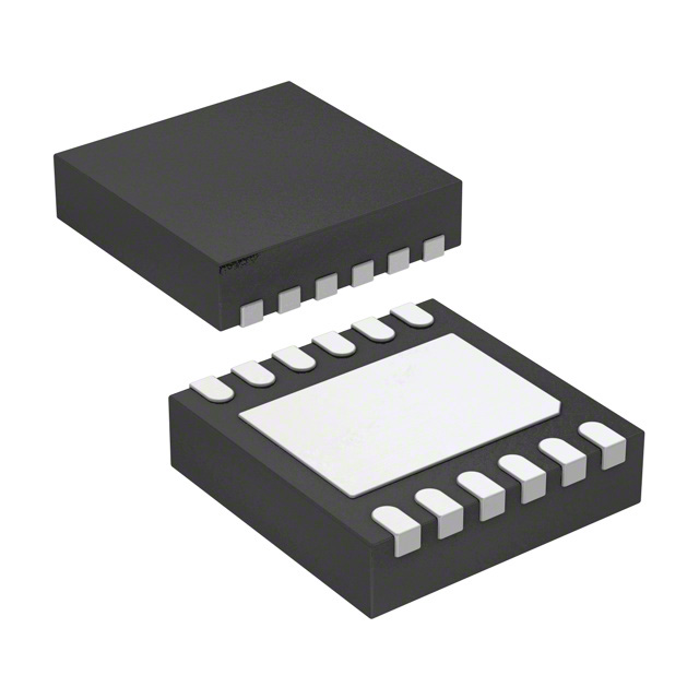
a compact 12-pin (3mm x 3mm) TDFN package. Simulation models are available.
Applications
●
●
●
●
●
●
Industrial Control Power Supplies
General Purpose Point-of-Load
Distributed Supply Regulation
Base Station Power Supplies
Wall Transformer Regulation
High Voltage Single-Board Systems
VOUT
VIN MA X17760 LX
EN/UVLO
SS
RT/SYNC
VCC
19-100795; Rev 0; 4/20
FB
EXTVCC
MODE
SGND
PGND
EP
RESET
VOUT
● Reduces Power Dissipation
• 93% Peak Efficiency
• PFM Mode Enables Enhanced Light-Load
Efficiency
• EXTVCC Bootstrap Input for Improved Efficiency
• 5μA Shutdown Current
● Operates Reliably in Adverse Industrial Environments
• Built-in Hiccup Mode Overload Protection
• Programmable Soft-Start and Prebiased Power-up
• Built-in Output-Voltage Monitoring with RESET
• Programmable EN/UVLO Threshold
• Overtemperature Protection
• CISPR 22 Class B Compliant
• Wide -40°C to +125°C Ambient Operating
Temperature Range/ -40°C to +150°C Junction
Temperature Range
Ordering Information appears at end of data sheet.
Simplified Application Circuit
VIN
● Reduces Number of DC-DC Regulators to Stock
• Wide 4.5V to 76V Input
• Adjustable Output Range from 0.8V up to 88% of
VIN
• Up to 300mA Output Current
• 200kHz, 300kHz, 400kHz, and 600kHz
Programmable Switching Frequency with External
Clock Synchronization.
�MAX17760
4.5V to 76V, 300mA, High-Efficiency, Synchronous
Step-Down DC-DC Converter
Absolute Maximum Ratings
VIN to SGND........................................................... -0.3V to +80V
EN/UVLO to SGND ....................... -0.3 to min((VIN + 0.3V), 26V)
EXTVCC to SGND.................................................. -0.3V to +26V
LX to PGND .................................................... -0.3 to (VIN + 0.3V)
FB, RESET, SS, MODE, VCC, RT/SYNC to SGND . -0.3V to +6V
PGND to SGND ..................................................... -0.3V to +0.3V
LX Total RMS Current ......................................................... ±0.6A
Continuous Power Dissipation (Multilayer Board) (TA = +70°C,
derate 24.4mW/°C above +70°C.) ...............................1951.2mW
Output Short-Circuit Duration......................................Continuous
Operating Temperature Range (Note 1) .............-40°C to +125°C
Junction Temperature ....................................................... +150°C
Storage Temperature Range ..............................-65°C to +150°C
Lead Temperature (soldering, 10s)................................... +300°C
Soldering Temperature (reflow) ........................................ +260°C
Note 1: Junction temperature greater than +125°C degrades operating lifetimes.
Stresses beyond those listed under “Absolute Maximum Ratings” may cause permanent damage to the device. These are stress ratings only, and functional operation of the
device at these or any other conditions beyond those indicated in the operational sections of the specifications is not implied. Exposure to absolute maximum rating conditions for
extended periods may affect device reliability.
Package Information
12 TDFN
Package Code
TD1233+1C
Outline Number
21-0664
Land Pattern Number
90-0397
Thermal Resistance, Four-Layer Board:
Junction to Ambient (θJA)
41°C/W
Junction to Case (θJC)
8.5°C/W
For the latest package outline information and land patterns (footprints), go to www.maximintegrated.com/packages. Note that a “+”, “#”, or “-” in the package code indicates
RoHS status only. Package drawings may show a different suffix character, but the drawing pertains to the package regardless of RoHS status.
Package thermal resistances were obtained using the method described in JEDEC specification JESD51-7, using a four-layer board. For detailed information on package thermal
considerations, refer to www.maximintegrated.com/thermal-tutorial.
Electrical Characteristics
(VIN = 24V, EN/UVLO = unconnected, RRT/SYNC = 69.8kΩ (fSW = 400 kHz), VMODE = VPGND = VSGND = VEXTVCC = 0V, CVCC =
1μF, VFB = 1V, LX = SS = RESET = unconnected, TA = TJ = -40°C to 125°C, unless otherwise noted. Typical values are at TA = +25°C.
All voltages are referenced to SGND, unless otherwise noted.) (Note 2 )
PARAMETER
SYMBOL
CONDITIONS
MIN
TYP
MAX
UNITS
76
V
10
μA
INPUT SUPPLY (VIN)
Input Voltage Range
Input Shutdown Current
Input Quiescent Current
VIN
IIN-SH
4.5
VEN/UVLO = 0V (shutdown mode)
2.5
5
IQ_PFM
MODE = Unconnected, VEXTVCC = 5V
75
μA
IQ_PWM
VFB = 0.75V, Normal switching mode
2.5
mA
ENABLE/UVLO (EN/UVLO)
EN/UVLO Threshold
EN/UVLO Pullup
Current
www.maximintegrated.com
VENR
VEN/UVLO rising
1.19
1.215
1.24
VENF
VEN/UVLO falling
1.09
1.115
1.14
V
VENT
VEN/UVLO falling, true shutdown
2.8
µA
IEN/UVLO
VEN/UVLO = 1.215V
19-100795
0.7
2.2
2.5
Maxim Integrated | 2
�MAX17760
4.5V to 76V, 300mA, High-Efficiency, Synchronous
Step-Down DC-DC Converter
Electrical Characteristics (continued)
(VIN = 24V, EN/UVLO = unconnected, RRT/SYNC = 69.8kΩ (fSW = 400 kHz), VMODE = VPGND = VSGND = VEXTVCC = 0V, CVCC =
1μF, VFB = 1V, LX = SS = RESET = unconnected, TA = TJ = -40°C to 125°C, unless otherwise noted. Typical values are at TA = +25°C.
All voltages are referenced to SGND, unless otherwise noted.) (Note 2 )
PARAMETER
SYMBOL
CONDITIONS
MIN
TYP
MAX
UNITS
4.75
5
5.25
V
13
26
52
mA
0.27
V
LINEAR REGULATOR (VCC)
VCC Output Voltage
Range
VCC Current Limit
VCC Dropout Voltage
VCC UVLO
VCC
6V ≤ VIN ≤ 76V, 0mA < IVCC < 5mA
IVCC-MAX
VCC = 4.3V, VIN = 12V
VCC-DO
VIN = 4.5V, IVCC = 5mA
VCC-UVR
VCC rising
4.05
4.2
4.35
VCC-UVF
VCC falling
3.65
3.8
3.95
EXTVCC Operating
Voltage Range
4.85
VEXTVCC rising
EXTVCC Switchover
Threshold
EXTVCC Dropout
Voltage
EXTVCC Current Limit
4.65
Hysteresis
EXTVCC-DO
24
4.74
4.85
0.3
VEXTVCC = 4.75V, IVCC = 5mA
13
V
V
V
0.1
V
21
34
mA
IVCC-MAX
VCC = 4.3V, VEXTVCC = 5V
High-Side pMOS OnResistance
RDS-ONH
ILX = 0.15A, sourcing
1.8
3.6
Ω
Low-Side nMOS OnResistance
RDS-ONL
ILX = 0.15A, sinking
0.55
1.1
Ω
LX Leakage Current
ILX-LKG
+1
μA
μA
POWER MOSFETS
VLX = (VPGND + 1V) to (VIN - 1V), TA =
+25°C
-1
SOFT-START (SS)
Charging Current
ISS
4.7
5
5.3
VMODE = 0V (PWM mode)
0.788
0.802
0.815
MODE = Unconnected (PFM mode)
0.788
0.813
0.827
TA = +25°C
-100
FEEDBACK (FB)
FB Regulation Voltage
FB Input Leakage
Current
VFB-REG
IFB
V
+100
nA
mA
CURRENT LIMIT
Peak Current Limit
Threshold
IPEAK-LIMIT
Negative Current Limit
Threshold
ISINK-LIMIT
PFM Current Limit
IPFM
VMODE = 0V (PWM mode)
532
640
755
238
270
302
MODE = Unconnected (PFM mode)
MODE = Unconnected
2.5
185
240
310
1
1.22
1.44
mA
mA
MODE
PFM Mode Threshold
VTH_PFM
Rising
Hysteresis
0.175
MODE Pullup Current at
Power-Up
www.maximintegrated.com
2.5
19-100795
V
μA
Maxim Integrated | 3
�MAX17760
4.5V to 76V, 300mA, High-Efficiency, Synchronous
Step-Down DC-DC Converter
Electrical Characteristics (continued)
(VIN = 24V, EN/UVLO = unconnected, RRT/SYNC = 69.8kΩ (fSW = 400 kHz), VMODE = VPGND = VSGND = VEXTVCC = 0V, CVCC =
1μF, VFB = 1V, LX = SS = RESET = unconnected, TA = TJ = -40°C to 125°C, unless otherwise noted. Typical values are at TA = +25°C.
All voltages are referenced to SGND, unless otherwise noted.) (Note 2 )
PARAMETER
SYMBOL
CONDITIONS
MIN
TYP
MAX
RRT/SYNC = 140kΩ
180
200
220
RRT/SYNC = 93.1kΩ
270
300
330
RRT/SYNC = 69.8kΩ
360
400
440
RRT/SYNC = 46.4kΩ
540
600
660
UNITS
OSCILLATOR (RT/SYNC)
Switching Frequency
fSW
Switching Frequency
Adjustable Range
Minimum On-Time
Maximum Duty Cycle
Hiccup Timeout Period
200
tON-MIN
DMAX
88
tHIC-TOUT
SYNC Threshold
600
kHz
70
110
ns
93
97
%
51
SYNC Frequency
Capture Range
1.15 x
fSW (typ)
VIH
kHz
ms
1.4 x
fSW (typ)
2.1
VIL
0.8
V
RESET
RESET Output Level
Low
IRESET = 10mA
RESET Output Leakage
Current
TA = +25°C
0.4
V
1
µA
FB Threshold for
RESET Deassertion
VFB-OKR
VFB rising
95
%
FB Threshold for
RESET Assertion
VFB-OKF
VFB falling
92
%
2.1
ms
RESET Delay after FB
Reaches 95%
Regulation
THERMAL SHUTDOWN
Thermal Shutdown
Threshold
Temperature rising
160
Hysteresis
20
°C
Note 2: Electrical specifications are production tested at TA = +25ºC. Specifications over the entire operating temperature range are
guaranteed by design and characterization.
www.maximintegrated.com
19-100795
Maxim Integrated | 4
�MAX17760
4.5V to 76V, 300mA, High-Efficiency, Synchronous
Step-Down DC-DC Converter
Typical Operating Characteristics
(VIN = 24V, VSGND = VPGND = 0V, CVCC = 1μF, EN/UVLO = unconnected, CSS = 5600pF, TA = +25°C, unless otherwise noted. All
voltages are referenced to SGND, unless otherwise noted.)
www.maximintegrated.com
19-100795
Maxim Integrated | 5
�MAX17760
4.5V to 76V, 300mA, High-Efficiency, Synchronous
Step-Down DC-DC Converter
Typical Operating Characteristics (continued)
(VIN = 24V, VSGND = VPGND = 0V, CVCC = 1μF, EN/UVLO = unconnected, CSS = 5600pF, TA = +25°C, unless otherwise noted. All
voltages are referenced to SGND, unless otherwise noted.)
www.maximintegrated.com
19-100795
Maxim Integrated | 6
�MAX17760
4.5V to 76V, 300mA, High-Efficiency, Synchronous
Step-Down DC-DC Converter
Typical Operating Characteristics (continued)
(VIN = 24V, VSGND = VPGND = 0V, CVCC = 1μF, EN/UVLO = unconnected, CSS = 5600pF, TA = +25°C, unless otherwise noted. All
voltages are referenced to SGND, unless otherwise noted.)
www.maximintegrated.com
19-100795
Maxim Integrated | 7
�MAX17760
4.5V to 76V, 300mA, High-Efficiency, Synchronous
Step-Down DC-DC Converter
Typical Operating Characteristics (continued)
(VIN = 24V, VSGND = VPGND = 0V, CVCC = 1μF, EN/UVLO = unconnected, CSS = 5600pF, TA = +25°C, unless otherwise noted. All
voltages are referenced to SGND, unless otherwise noted.)
www.maximintegrated.com
19-100795
Maxim Integrated | 8
�MAX17760
4.5V to 76V, 300mA, High-Efficiency, Synchronous
Step-Down DC-DC Converter
Pin Configuration
TOP VIEW
1
PGND
2
VCC
3
EN/UVLO
4
RESET
5
RT/SYNC
6
+
VIN
12 LX
11 SGND
10 MODE
MA
MAX
X17760
EP
9
SS
8
FB
7
EXTVCC
TDFN
(3mm x 3mm
3mm))
Pin Description
PIN
NAME
FUNCTION
1
VIN
Power Supply Input Pin. 4.5V to 76V input-supply range. Decouple to PGND with a 1μF capacitor.
Place the capacitor close to the VIN and PGND pins.
2
PGND
3
VCC
4
EN/UVLO
5
RESET
Open-Drain RESET Output. The RESET output is driven low when FB drops below 92% of its set
value. RESET goes high 2.1ms after FB rises above 95% of its set value.
6
RT/SYNC
Programmable Switching Frequency and External Clock Synchronization Input. Connect a resistor
from RT/SYNC to SGND to set the converter's switching frequency between 200kHz and 600kHz.
An external clock can be connected to the RT/SYNC to synchronize the device with an external
clock in PWM mode. See the Switching Frequency Selection and External Clock Synchronization
(RT/SYNC) section for more details.
7
EXTVCC
External Power Supply Input for the EXT-LDO. Connect EXTVCC to the buck converter output for
an output voltage between 5V and 24V. When EXTVCC is not used, connect it to SGND. See the
Linear Regulator (VCC and EXTVCC) section for more details.
8
FB
Feedback Input. Connect FB to the center node of an external resistor-divider from the output to
SGND to set the output voltage. See the Adjusting Output Voltage section for more details.
9
SS
Soft-Start Input. Connect a capacitor from SS to SGND to set the soft-start time.
10
MODE
MODE Selection. The MODE pin configures the device to operate either in PWM or PFM mode of
operation. Leave MODE unconnected for PFM operation. Connect MODE to SGND for constantfrequency PWM operation at all loads.
11
SGND
Signal Ground.
12
LX
Switching Node. Connect LX pin to the switching-side of the inductor.
—
EP
Exposed Pad. Connect EP to SGND. Refer to the MAX17760 EV kit data sheet for the
recommended method of PCB layout, routing, and thermal vias.
www.maximintegrated.com
Power Ground. Refer to the MAX17760 EV kit data sheet for the recommended PCB layout and
routing.
5V LDO Output. Bypass VCC with a 1μF ceramic capacitor to PGND. LDO doesn't support external
loading on VCC.
Enable/Undervoltage Lockout Pin. Drive EN/UVLO high to enable the output. Connect to the
center of a resistor-divider between VIN and SGND to set the input voltage at which the device
turns on. Leave the pin unconnected for always-on operation.
19-100795
Maxim Integrated | 9
�MAX17760
4.5V to 76V, 300mA, High-Efficiency, Synchronous
Step-Down DC-DC Converter
Functional Block Diagram
M A X 17760
EXTVCC
EXT-LDO
VIN
INT-LDO
VCC
BIAS SELECT
VIN
POK
2.5μA
EN/UVLO
PEAK-LIMIT
CHIPEN
CURRENTSENSE LOGIC
1.215V
CS
CURRENTSENSE
AMPLIFIER
PFM
THERMAL SHUTDOWN
DH
CLK
RT/SYNC
OSCILLATOR
SLOPE
VCC
HIGH-SIDE
DRIVER
LX
PFM/PWM
CONTROL LOGIC
DL
LOW-SIDE
DRIVER
2.5μA
*S1
PGND
MODE
MODE SELECT
*S2
1.22V
CS
FB
SS
EXTERNAL
SOFT-START
CONTROL
ISINK-LIMIT
SLOPE
20kΩ
++
NEGATIVE
CURRENT LIMIT
RESET
PWM
ERROR
AMPLIFIER
CHIPEN
0.76V
RESET
LOGIC
FB
CLK
www.maximintegrated.com
*S1 – CLOSE, S2 – OPEN when CHIPEN = 0
*S1 – OPEN, S2 – CLOSE when CHIPEN = 1
19-100795
Maxim Integrated | 10
�MAX17760
4.5V to 76V, 300mA, High-Efficiency, Synchronous
Step-Down DC-DC Converter
Detailed Description
The MAX17760 is a high-efficiency, high voltage, synchronous step-down DC-DC converter with integrated MOSFETs
operating over an input-voltage range of 4.5V to 76V. The device can deliver up to 300mA current. Output voltage
is programmable from 0.8V up to 88% of VIN. Built-in control loop compensation eliminates the need for external
components. The feedback-voltage regulation accuracy over -40°C to +125°C is +1.6% to -1.7%.
The device features a peak-current-mode control architecture. An internal transconductance error amplifier produces an
integrated error voltage at an internal node, which sets the duty cycle using a PWM comparator, a high-side currentsense amplifier, and a slope-compensation generator. At each rising edge of the clock, the high-side MOSFET turns
on and remains on until either the appropriate or maximum duty cycle is reached, or the peak current limit is detected.
During the high-side MOSFET on-time, the inductor current ramps up. During the rest of the switching cycle, the highside MOSFET turns off and the low-side MOSFET turns on. The inductor releases the stored energy as its current ramps
down and provides current to the output. The internal low RDSON pMOS/nMOS switches ensure high efficiency at full
load.
The MAX17760 features a MODE pin that can be used to program the device in PWM or PFM control schemes. The
device also features adjustable-input undervoltage lockout (EN/UVLO), adjustable soft-start (SS), open-drain RESET,
and external clock synchronization (RT/SYNC) features. The MAX17760 offers a low minimum on-time that allows to
operate for a wide range of input supply at a given switching frequency.
Mode Selection
The MAX17760 supports PWM and PFM mode of operation. The device detects the MODE pin status at power-up and
latches the MODE of operation. Leave the MODE pin unconnected for PFM operation. At power-up the MAX17760 pullup
the MODE pin with a 2.5μA current. If the MODE pin exceeds the PFM mode threshold (VTH_PFM), the part latches PFM
mode and pulls down MODE with a 20kΩ internal resistor. Connect MODE to SGND for constant-frequency forced PWM
operation at all loads. The mode of operation cannot be changed on-the-fly after power-up.
In PWM mode, the inductor current is allowed to go negative. PWM operation provides constant frequency operation
irrespective of loading, and is useful in applications sensitive to switching frequency.
PFM mode provides high efficiency at light load conditions by disabling negative inductor current and additionally skipping
pulses. In PFM mode, the inductor current is forced to a fixed peak of IPFM (240mA typ) every clock cycle until the
output rises to 102.3% of the set nominal output voltage. Once the output reaches 102.3% of the set nominal output
voltage, both the high-side and low-side FETs are turned off and the device enters hibernation until the load discharges
the output to 101.1% of the set nominal output voltage. Most of the internal blocks are turned off in hibernate operation
to reduce quiescent current. After the output falls below 101.1% of the set nominal output voltage, the device comes out
of hibernate operation, turns on all internal blocks, and again commences the process of delivering pulses of energy to
the output until it reaches 102.3% of the set nominal output voltage. The advantage of PFM mode is higher efficiency at
light loads because of lower quiescent current drawn from supply. However, the output voltage ripple is higher compared
to PWM mode of operation and switching frequency is not constant at light loads.
www.maximintegrated.com
19-100795
Maxim Integrated | 11
�MAX17760
4.5V to 76V, 300mA, High-Efficiency, Synchronous
Step-Down DC-DC Converter
Linear Regulator (VCC and EXTVCC)
The MAX17760 integrates two internal low-dropout (LDO) linear regulators INT-LDO and EXT-LDO that power VCC. INTLDO is powered from VIN and turns on when VEN/UVLO > VENT (0.7V typ). EXT-LDO is powered from EXTVCC. At
any time, only one of these two linear regulators operates, depending on the EXTVCC voltage. If EXTVCC is greater
than 4.74V (typ), VCC is powered from the EXTVCC. If EXTVCC is lower than 4.44V (typ), VCC is powered from VIN.
Powering VCC from EXTVCC increases efficiency at higher input voltages. Typical VCC output voltage is 5V. Bypass
VCC to SGND with a 1µF low-ESR ceramic capacitor. VCC powers the internal blocks and both low-side and high-side
MOSFET drivers.
The MAX17760 employs an undervoltage-lockout circuit that forces the converter off when VCC voltage falls below VCCUVF (3.8V typ). The buck converter enables when the VCC voltage rises above VCC-UVR (4.2 typ).
EXTVCC should be connected to the output capacitor with an R-C filter as shown in Figure 4. Without this R-C filter, the
absolute maximum rating of EXTVCC (-0.3V) can be exceeded under short-circuit conditions, due to oscillations between
the ceramic output capacitor and the inductance of the short-circuit path. In general, parasitic board or wiring inductance
should be minimized and the output voltage under short-circuit operation should be verified to ensure that the absolute
maximum rating of EXTVCC is not exceeded.
Switching Frequency Selection and External Clock Synchronization (RT/SYNC)
The MAX17760 can be programmed to one of the four discrete switching frequencies 200KHz, 300kHz, 400kHz, and
600kHz, by connecting a resistor from RT/SYNC to SGND. Table 1 provides resistor values for different switching
frequencies.
The MAX17760 can be synchronized to an external clock coupled to the RT/SYNC pin through a 22pF capacitor as
shown in Figure 1. The external clock must be applied after RESET is asserted high for proper configuration of the
internal loop compensation. If the external clock frequency is within the allowed SYNC frequency range (1.15 to 1.4 times
the nominal internal clock frequency fSW), the internal clock synchronizes to the external clock within 1 clock cycle. The
allowed external clock duty cycle range is 10% to 80%.
Table 1. Switching Frequency vs. RT/SYNC Resistor
SWITCHING FREQUENCY (kHz)
RRT/SYNC (kΩ)
200
140
300
93.1
400
69.8
600
46.4
22pF
RT/SYNC
EXTERNAL
CLOCK
SOURCE
RRT/SYNC
M A X 17760
SGND
Figure 1. External Clock Synchronization
www.maximintegrated.com
19-100795
Maxim Integrated | 12
�MAX17760
4.5V to 76V, 300mA, High-Efficiency, Synchronous
Step-Down DC-DC Converter
Operating Input Voltage Range
The minimum and maximum operating input voltages for a given output-voltage setting should be calculated as follows:
VIN(MIN) =
(
(
VOUT + IOUT MAX × RDCR(MAX) + RDS-ONL(MAX)
(
)
DMAX
)) + (I
OUT(MAX) × (RDS-ONH(MAX)-RDS-ONL(MAX)))
VOUT
VIN(MAX) = f
SW(MAX) × tON-MIN(MAX)
where:
VOUT = Steady-state output voltage
IOUT(MAX) = Maximum load current
RDCR(MAX) = Worst-case DC resistance of the inductor
fSW(MAX) = Maximum switching frequency
DMAX = Minimum specification of maximum duty ratio (0.88)
tON-MIN(MAX) = Worst-case minimum switch on-time (110 ns)
RDS-ONL(MAX) and RDS-ONH(MAX) = Worst-case on-state resistances of low-side and high-side internal MOSFETs,
respectively.
Overcurrent Protection/Hiccup Mode
The device features a hysteretic peak current-limit protection scheme to protect the internal FETs and inductor under
output short-circuit conditions. When the inductor peak current exceeds IPEAK-LIMIT, the high-side switch is turned off
and the low-side switch is turned on. After the current is reduced to 290mA (typ), the high-side switch is turned on at the
rising edge of the next clock pulse. The device enters a hiccup timeout period tHIC_TOUT (51ms typ) if 16 consecutive
peak current limit events are detected. After the hiccup time-out period has elapsed, the device restarts. If the overcurrent
condition persists, the device remains in hiccup current limit mode until the overcurrent fault is removed.
RESET Output
The device features a RESET comparator to monitor the output voltage. The open-drain RESET output requires an
external pullup resistor. RESET goes high 2.1ms after the regulator output increases above 95% of the designed nominal
regulated voltage. RESET goes low when the regulator output voltage drops to below 92% of the nominal regulated
voltage. RESET also goes low during thermal shutdown.
Prebiased Output
When the device starts into a prebiased output, both the high-side and the low-side switches are turned off so that the
converter does not sink current from the output. High-side and low-side switches do not start switching until the PWM
comparator commands the first PWM pulse, at which point switching commences. The output voltage is then smoothly
ramped up to the target value in alignment with the internal reference.
Thermal-Shutdown Protection
Thermal shutdown protection limits junction temperature of the device. When the junction temperature of the device
exceeds +160°C, an on-chip thermal sensor shuts down the device, allowing the device to cool. The thermal sensor turns
the device on with soft-start after the junction temperature cools by 20°C. Carefully evaluate the total power dissipation
(see the Power Dissipation section) to avoid unwanted triggering of the thermal shutdown protection in normal operation.
www.maximintegrated.com
19-100795
Maxim Integrated | 13
�MAX17760
4.5V to 76V, 300mA, High-Efficiency, Synchronous
Step-Down DC-DC Converter
Applications Information
Input Capacitor Selection
The input filter capacitor reduces peak currents drawn from the power source and reduces noise and voltage ripple on
the input caused by the circuit switching. The input capacitor RMS current requirement (IRMS) is defined by the following
equation:
IRMS= IOUT(MAX)×
√VOUT × (VIN − VOUT)
VIN
where, IOUT(MAX) is the maximum load current. IRMS has a maximum value when the input voltage equals twice the
output voltage (VIN = 2 x VOUT), so
IRMS(MAX) =
IOUT(MAX)
2
.
Choose an input capacitor that exhibits less than +10°C temperature rise at the RMS input current for optimal longterm reliability. Use low-ESR ceramic capacitors with high-ripple-current capability at the input. X7R capacitors are
recommended in industrial applications for their temperature stability. Calculate the input capacitance using the following
equation:
CIN =
(
IOUT MAX × D × 1 − D
(
)
η × fSW × ∆ VIN
)
where:
D = VOUT/VIN and is the duty ratio of the controller
fSW = Switching frequency
ΔVIN = Allowable input-voltage ripple
η = Efficiency
In applications where the source is located distant from the device input, an appropriate electrolytic capacitor should
be added in parallel to the ceramic capacitor to provide necessary damping for potential oscillations caused by the
inductance of the longer input power path and input ceramic capacitor.
Inductor Selection
Three key inductor parameters must be specified for operation with the device: inductance value (L), inductor saturation
current (ISAT) and DC resistance (RDCR). The switching frequency and output voltage determine the inductor value as
follows:
L=
4 × VOUT
fSW
where VOUT = Output voltage
fSW = Switching frequency
Select a low-loss inductor closest to the calculated value with acceptable dimensions and having the lowest possible DC
resistance. The saturation current rating (ISAT) of the inductor must be high enough to ensure that saturation can occur
only above the peak current-limit value.
www.maximintegrated.com
19-100795
Maxim Integrated | 14
�MAX17760
4.5V to 76V, 300mA, High-Efficiency, Synchronous
Step-Down DC-DC Converter
Output Capacitor Selection
X7R ceramic output capacitors are preferred due to their stability over temperature in industrial applications. The output
capacitors are sized to support a step load of 50% of the maximum output current in the application, so the output-voltage
deviation is contained to 3% of the output-voltage change. The minimum required output capacitance can be calculated
as follows:
1
COUT = 2 ×
ISTEP × tRESPONSE
∆ VOUT
0.35
tRESPONSE ≅ f
C
where:
ISTEP = Load current step
tRESPONSE = Response time of the controller
ΔVOUT = Allowable output-voltage deviation
fC = Target closed-loop crossover frequency
fSW = Switching frequency.
Select fC to be the minimum of 1/10th of fSW and 30kHz. Actual derating of ceramic capacitors with DC-bias voltage
must be considered while selecting the output capacitor. Derating curves are available from all major ceramic capacitor
manufacturers.
Soft-Start Capacitor Selection
The device implements adjustable soft-start operation to reduce inrush current. A capacitor connected from the SS pin
to SGND programs the soft-start time. The selected output capacitance (CSEL) and the output voltage (VOUT) determine
the minimum required soft-start capacitor as follows:
CSS ≥ 30 × 10 − 6 × CSEL × VOUT
The soft-start time (tSS) is related to the capacitor connected at SS (CSS) by the following equation:
tSS =
CSS
6.25 × 10 − 6
For example, to program a 0.9ms soft-start time, a 5.6nF capacitor should be connected from the SS pin to SGND. Note
that, during startup, the device operates at half the programmed switching frequency until the output voltage reaches
80% of set output nominal voltage.
www.maximintegrated.com
19-100795
Maxim Integrated | 15
�MAX17760
4.5V to 76V, 300mA, High-Efficiency, Synchronous
Step-Down DC-DC Converter
Setting the Input Undervoltage-Lockout Level
Drive EN/UVLO high to enable the output. Leave the pin unconnected for always-on operation. Set the voltage at which
each converter turns on with a resistive voltage-divider connected from VIN to SGND (see Figure 2). Connect the center
node of the divider to EN/UVLO pin.
Choose R1 as follows:
R1 ≤ (110000 × VINU)
where VINU is the input voltage at which the MAX17760 is required to turn on and R1 is in Ω. Calculate the value of R2
as follows:
R2 =
R1 × 1.215
(VINU − 1.215 + (2.5μ × R1))
VIN
R1
EN/UVLO
R2
SGND
Figure 2. Setting the Input Undervoltage Lockout Level
www.maximintegrated.com
19-100795
Maxim Integrated | 16
�MAX17760
4.5V to 76V, 300mA, High-Efficiency, Synchronous
Step-Down DC-DC Converter
Adjusting Output Voltage
Set the output voltage with a resistive voltage-divider connected from the output voltage node (VOUT) to SGND (see
Figure 3). Connect the center node of the divider to the FB pin. Use the following procedure to choose the resistive
voltage-divider values:
Calculate resistor R3 from the output to the FB pin as follows:
R3 =
15 × VOUT
0.8
where R3 is in kΩ.
Calculate resistor R4 from the FB pin to SGND as follows:
R4 =
R3 × 0.8
(VOUT- 0.8)
R4 is in kΩ.
VOUT
R3
FB
R4
SGND
Figure 3. Adjusting Output Voltage
Power Dissipation
At a particular operating condition, the power losses that lead to a temperature rise of the device are estimated as follows:
(
( 1 )) (
PLOSS = POUT × η − 1 − IOUT2 × RDCR
POUT = VOUT × IOUT
)
where:
POUT = Output power
η = Efficiency of the converter
RDCR = DC resistance of the inductor (see the Typical Operating Characteristics for more information on efficiency at
typical operating conditions).
For a typical multilayer board, the thermal performance metrics for the package are given below:
θJA = 41ºC/W
θJC = 8.5ºC/W
The junction temperature of the device can be estimated at any given maximum ambient temperature (TA(MAX)) from the
following equation:
TJ(MAX) = TA(MAX) + (θJA × PLOSS)
www.maximintegrated.com
19-100795
Maxim Integrated | 17
�MAX17760
4.5V to 76V, 300mA, High-Efficiency, Synchronous
Step-Down DC-DC Converter
If the application has a thermal-management system that ensures that the exposed pad of the device is maintained at a
given temperature (TEP(MAX)) by using proper heat sinks, then the junction temperature of the device can be estimated
at any given maximum ambient temperature as:
TJ(MAX) = TEP(MAX) + (θJC × PLOSS)
Note: Junction temperatures greater than +125°C degrades operating lifetimes.
PCB Layout Guidelines
All connections carrying pulsed currents must be very short and as wide as possible. The inductance of these
connections must be kept to an absolute minimum due to the high di/dt of the currents. Since inductance of a currentcarrying loop is proportional to the area enclosed by the loop, if the loop area is made very small, inductance is reduced.
Additionally, small-current loop areas reduce radiated EMI.
A ceramic input filter capacitor should be placed close to the VIN pins of the IC. This eliminates as much trace inductance
effects as possible and gives the IC a cleaner voltage supply. A bypass capacitor for the VCC pin also should be placed
close to the pin to reduce effects of trace impedance.
When routing the circuitry around the IC, the analog small signal ground and the power ground for switching currents
must be kept separate. They should be connected together at a point where switching activity is minimum. This helps
keep the analog ground quiet. The ground plane should be kept continuous (unbroken) as far as possible. No trace
carrying high switching current should be placed directly over any ground plane discontinuity.
PCB layout also affects the thermal performance of the design. A number of thermal throughputs that connect to a large
ground plane should be provided under the exposed pad of the device for efficient heat dissipation.
For a sample layout that ensures first pass success, refer to the MAX17760 EV Kit layout available at
www.maximintegrated.com.
Typical Application Circuits
VIN
(7V TO 76V)
C1
1μF
LX
EN/UVLO
SS
56μH
PGND
M A X 17760
R5
69.8kΩ
C2
1μF
VCC
C5
0.1μF
MODE
EP
R3
95.3kΩ
VOUT
R6
EXTVCC
SGND
C4
10μF
FB
RT/SYNC
C3
5600pF
VOUT
5V, 300mA
L1
VIN
22Ω
R4
18.2kΩ
fSW = 400kHz:
L1 = 56µH/4.8mm x 4.8mm, 0.7A (WURTH 74408943560)
C1 = 1µF/100V/X7R/1206 (TDK C3216X7R2A105K160AA)
C4 = 10µF/16V/X7R/0805 (MURATA GRM21BZ71C106KE15)
MODE:
1. CONNECT TO SGND FOR PWM MODE
2. LEAVE UNCONNECTED FOR PFM MODE
RESET
Figure 4. 5V Output with 400kHz Switching Frequency
www.maximintegrated.com
19-100795
Maxim Integrated | 18
�MAX17760
4.5V to 76V, 300mA, High-Efficiency, Synchronous
Step-Down DC-DC Converter
Typical Application Circuits (continued)
VIN
(5V TO 76V)
C1
1μF
VOUT
3.3V, 300mA
L1
VIN
LX
EN/UVLO
SS
33μH
PGND
M A X 17760
C4
22μF
R3
59.0kΩ
FB
RT/SYNC
C3
5600pF
R5
69.8kΩ
C2
1μF
EXTVCC
R4
18.7kΩ
VCC
fSW = 400kHz:
L1 = 33µH/4.8mm x 4.8mm, 0.9A (WURTH 74408943330)
C1 = 1µF/100V/X7R/1206 (TDK C3216X7R2A105K160AA)
C4 = 22µF/6.3V/X7R/0805 (MURATA GRM21BZ70J226ME44)
MODE:
1. CONNECT TO SGND FOR PWM MODE
2. LEAVE UNCONNECTED FOR PFM MODE
MODE
EP
SGND
RESET
Figure 5. 3.3V Output with 400kHz Switching Frequency
VIN
(16V TO 76V)
C1
1μF
LX
EN/UVLO
SS
100μH
PGND
M A X 17760
R5
69.8kΩ
C2
1μF
VCC
C5
0.1μF
MODE
EP
R3
226kΩ
VOUT
R6
EXTVCC
SGND
C4
4.7μF
FB
RT/SYNC
C3
5600pF
VOUT
12V, 300mA
L1
VIN
22Ω
R4
16.2kΩ
fSW = 400kHz:
L1 = 100µH/4.8mm x 4.8mm, 0.52A (WURTH 74408943101)
C1 = 1µF/100V/X7R/1206 (TDK C3216X7R2A105K160AA)
C4 = 4.7µF/35V/X7R/1206 (TDK C3216X7R1V475K160AB)
MODE:
1. CONNECT TO SGND FOR PWM MODE
2. LEAVE UNCONNECTED FOR PFM MODE
RESET
Figure 6. 12V Output with 400kHz Switching Frequency
www.maximintegrated.com
19-100795
Maxim Integrated | 19
�MAX17760
4.5V to 76V, 300mA, High-Efficiency, Synchronous
Step-Down DC-DC Converter
Ordering Information
TEMP. RANGE
PIN-PACKAGE
MAX17760ATC+
PART NUMBER
-40°C to +125°C
12 TDFN - EP* (3mm x 3mm)
MAX17760ATC+T
-40°C to +125°C
12 TDFN - EP* (3mm x 3mm)
+Denotes a lead(Pb)-free/RoHS-compliant package.
*EP = Exposed pad.
T = Tape and reel.
www.maximintegrated.com
19-100795
Maxim Integrated | 20
�MAX17760
4.5V to 76V, 300mA, High-Efficiency, Synchronous
Step-Down DC-DC Converter
Revision History
REVISION
NUMBER
REVISION
DATE
0
4/20
DESCRIPTION
Initial release
PAGES
CHANGED
—
For pricing, delivery, and ordering information, please visit Maxim Integrated’s online storefront at https://www.maximintegrated.com/en/storefront/storefront.html.
Maxim Integrated cannot assume responsibility for use of any circuitry other than circuitry entirely embodied in a Maxim Integrated product. No circuit patent
licenses are implied. Maxim Integrated reserves the right to change the circuitry and specifications without notice at any time. The parametric values (min and max
limits) shown in the Electrical Characteristics table are guaranteed. Other parametric values quoted in this data sheet are provided for guidance.
Maxim Integrated and the Maxim Integrated logo are trademarks of Maxim Integrated Products, Inc.
© 2020 Maxim Integrated Products, Inc.
�


 工商网监
湘ICP备2023018690号
工商网监
湘ICP备2023018690号
