19-1382; Rev 1; 9/99
MAX2660/MAX2661/MAX2663/MAX2671
Evaluation Kits
Each EV kit is shipped with a Maxim device configured
for operation with an IF input frequency of 40MHz to
500MHz, and LO input frequency of 600MHz to
2400MHz. The output matching network of each kit is
optimized for an RF output frequency of 900MHz.
Features
♦ +2.7V to +5.5V Single Supply
♦ Output Matched to 50Ω at 900MHz
♦ Optimal Component Placement
♦ Easy Evaluation of All Product Functions
♦ All Critical Peripheral Components Included
Ordering Information
Component List
DESIGNATION QTY
DESCRIPTION
COMPONENTS COMMON TO ALL EVALUATION KITS
C1, C2, C5,
C8, C9
5
220pF ±10% (0603) NP0 ceramic
capacitors
C3, C4, C7
3
47pF ±10% (0603) NP0 ceramic
capacitors
C10
1
10µF ±20%, 6.3V A-size tantalum
capacitor
J1, J2, J3
3
SMA connectors
JU1
1
3-pin header, 0.025” sq., 0.10" centers
L1
1
33nH inductor
L2
1
18nH inductor
R1
1
100Ω 5% (0603) resistor
MAX2660 EV KIT ADDITIONAL COMPONENTS
C6
U1
1
1pF ±0.1pF (0603) NP0 ceramic
capacitor
1
MAX2660, SOT23-6, upconverter
mixer
TEMP. RANGE
PIN-PACKAGE
MAX2660EVKIT-T
PART
-40°C to +85°C
6 SOT23-6
MAX2661EVKIT-T
-40°C to +85°C
6 SOT23-6
MAX2663EVKIT-T
-40°C to +85°C
6 SOT23-6
MAX2671EVKIT-T
-40°C to +85°C
6 SOT23-6
Component Suppliers
SUPPLIER
PHONE
FAX
AVX
803-946-0690
803-626-3123
Toko
847-297-0700
847-699-7864
_________________________Quick Start
Each EV kit is fully assembled and factory tested.
Follow the instructions in the Connections and Setup
section.
MAX2661 EV KIT ADDITIONAL COMPONENTS
C6
1
1pF ±0.1pF (0603) NP0 ceramic
capacitor
U1
1
MAX2661, SOT23-6, upconverter
mixer
MAX2663 EV KIT ADDITIONAL COMPONENTS
C6
1
1.8pF ±0.1pF (0603) NP0 ceramic
capacitor
U1
1
MAX2663, SOT23-6, upconverter
mixer
MAX2671 EV KIT ADDITIONAL COMPONENTS
C6
1
1pF ±0.1pF (0603) NP0 ceramic
capacitor
U1
1
MAX2671, SOT23-6, upconverter
mixer
Test Equipment Required
EQUIPMENT
DESCRIPTION
DC Power Supply
Capable of supplying +2.7V to
+5.5V at a minimum of 50mA
HP 8561E Spectrum
Analyzer
Or equivalent high-sensitivity
spectrum analyzer
Digital multimeters
To monitor supply voltage and
supply current (if desired)
HP 8648C RF Generators,
2
For the IFIN and LO inputs or
equivalent sine-wave sources
________________________________________________________________ Maxim Integrated Products
1
For free samples & the latest literature: http://www.maxim-ic.com, or phone 1-800-998-8800.
For small orders, phone 1-800-835-8769.
Evaluates: MAX2660/MAX2661/MAX2663/MAX2671
General Description
The MAX2660/MAX2661/MAX2663/MAX2671 evaluation
kits simplify evaluation of the MAX2660/MAX2661/
MAX2663/MAX2671 upconverter mixers. They enable testing of all the functions, with no additional support circuitry.
Signal inputs and outputs use SMA connectors and are
compatible with the 50Ω impedance of test equipment.
�Evaluates: MAX2660/MAX2661/MAX2663/MAX2671
MAX2660/MAX2661/MAX2663/MAX2671
Evaluation Kits
Connections and Setup
1) Verify the DC power supply is set to less than +5.5V
before attaching the supply to the EV kit. A good
starting voltage is +3.0V.
2) Verify the SHDN jumper is in the “VCC” position.
3) Connect a signal generator to the IFIN connector
using an SMA cable. As with any precision RF connector, be careful while threading the connector. For
optimal performance, consult the connector manufacturer’s specifications for torque recommendation.
Set the generator’s output to 70MHz at -30dBm
power level.
4) Connect a second signal generator to the LO input
connector using an SMA cable. Set the generator’s
output to 970MHz at -5dBm power level (use
-10dBm for the MAX2671 EV Kit).
5) Connect the RF output of the EV kit to the spectrum
analyzer using an SMA cable. Take care to use quality connector adapters for the spectrum analyzer’s
input. Avoid using BNC-type connectors due to their
high VSWR while operating in the gigahertz range.
6) To assist in troubleshooting, verify the correct voltages on the PC board with a multimeter. Use Table 1
to verify correct node voltage during proper operation.
PIN NAME
NOMINAL DC VOLTAGE (V)
1
LO
2
GND
0
3
IFIN
+1.37
4
RF OUT
5
VCC
6
SHDN
(VCC - 0.4) to (VCC - 1.0)
CONVERSION GAIN (dB) AT 900MHz
MAX2660
+7.0
MAX2661
+10.7
MAX2663
+3.4
MAX2671
+11.2
Detailed Description
Figure 1 is the schematic for the EV kit as shipped. The
output matching components, L1, L2, C5, and C6, are
optimized for an output frequency of 900MHz.
Capacitors C1 and C2 are DC blocking capacitors for
the IFIN and LO input ports. To reduce the possibility of
noise pickup, resistor R1 and capacitor C8 form a lowpass filter at the SHDN pin.
Capacitors C3, C4, C7, C9, and C10 form the V CC
decoupling network. Note the location of each component. Capacitor C10, a 10µF tantalum type, is located
near the VCC input test point. This serves as the central
node for distribution of VCC to the mixer’s supply pin
and the output pull-up inductor L2. Both of these supply points need separate bypass capacitors as well as
separate traces on the PC board. This is prudent practice to curtail crosstalk in high-frequency systems.
The EV kit is easily configured for use with any of the
MAX2660/MAX2661/MAX2663/MAX2671 devices. Each
of these devices offers different performance levels for
system optimization.
Changing to Different Devices
VCC
+2.7 to +5.5
VCC for normal operation
Analysis
1) Set the spectrum analyzer’s center frequency to
900MHz, with a span of 30MHz.
2) Set the marker position to the peak level.
3) Read the output power of the center frequency. This
should be -28dBm to -21dBm, depending on which
device is used. The output frequency is equal to the
algebraic difference of the LO and IF frequencies.
The power is equal to the IFIN input power plus the
conversion gain of the upconverter mixer. See Table
2 for the typical conversion gain of each device.
2
PART
Modifying the EV Kit
Table 1. Nominal DC Voltages
PIN NUMBER
Table 2. Typical Conversion Gain
To configure the EV kit for a different device, use
appropriate surface-mount rework equipment to
remove the existing IC from the PCB. Take care to
ensure that the package temperature does not exceed
the limits listed in the Absolute Maximum Ratings section of the MAX2660/MAX2661/MAX2663/MAX2671/
MAX2673 data sheet. Install the new device using
appropriate surface-mount equipment and techniques.
See Table 3 for the correct component values for the
desired operating frequency and device type.
Operation at Other Frequencies
Changing the EV kit to operate at frequencies other
than listed in Table 3 involves matching each device’s
output impedance to 50Ω at the frequency of interest.
_______________________________________________________________________________________
�MAX2660 Evaluation Kit
Evaluates: MAX2660/MAX2661/MAX2663/MAX2671
Table 3. Output Matching Components vs. RF Output Frequency
PART
MAX2660
MAX2661
MAX2663
MAX2671
COMPONENT
COMPONENT VALUE AT A GIVEN RF OUTPUT FREQUENCY (MHz)
AT 400
AT 900
AT 1900
AT 2450
L1 (nH)
Short
33
8.2
3.3
L2 (nH)
39
18
2.7
2.2
C3 (pF)
220
47
47
47
47
C4 (pF)
220
47
47
C5 (pF)
3300
220
220
15
C6 (pF)
6.8
1
1.5
Open
C7 (pF)
470
47
47
47
L1 (nH)
Short
33
8.2
3.3
L2 (nH)
39
18
2.7
1.8
C3 (pF)
470
47
47
47
C4 (pF)
220
47
47
47
C5 (pF)
3300
220
100
220
C6 (pF)
6.8
1
1.5
Open
C7 (pF)
470
47
47
47
L1 (nH)
Short
33
8.2
3.3
L2 (nH)
39
18
1.8
1.8
C3 (pF)
220
47
47
47
C4 (pF)
220
47
47
47
C5 (pF)
3300
220
100
220
C6 (pF)
6.8
1.8
1.8
Open
C7 (pF)
220
47
47
47
L1 (nH)
Short
33
8.2
3.3
L2 (nH)
39
18
2.7
1.8
C3 (pF)
220
47
47
47
C4 (pF)
220
47
47
47
C5 (pF)
3300
220
100
220
C6 (pF)
6.8
1
1.5
Open
C7 (pF)
220
47
47
47
_______________________________________________________________________________________
3
�Evaluates: MAX2660/MAX2661/MAX2663/MAX2671
MAX2660/MAX2661/MAX2663/MAX2671
Evaluation Kits
VCC
C10
CAPAVX
10µF
16V
C9
220pF
1
VCC
J1
R1
100
1
2
J2
3
SMA
C2
220pF
3
2
C1
220pF
SMA
JU1
LO
U1
SHDN
MAX2660
GND
IFIN
VCC
RFOUT
6
C8
220pF
5
4
VCC
C4
47pF
C3
47pF
L1
33nH
C5
220pF
J3
SMA
C6
L2
18nH
VCC
C7
47pF
Figure 1. MAX2660 EV Kit Schematic
4
_______________________________________________________________________________________
�MAX2660 Evaluation Kit
Evaluates: MAX2660/MAX2661/MAX2663/MAX2671
1.0"
Figure 2. MAX2660 EV Kit PC Board Layout—Component Side
_______________________________________________________________________________________
5
�Evaluates: MAX2660/MAX2661/MAX2663/MAX2671
MAX2660/MAX2661/MAX2663/MAX2671
Evaluation Kits
1.0"
Figure 3. MAX2660 EV Kit PC Board Layout—Component
Side Metal
6
1.0"
Figure 4. MAX2660 EV Kit PC Board Layout—Solder Side
Metal
_______________________________________________________________________________________
�
很抱歉,暂时无法提供与“MAX2660EVKIT+”相匹配的价格&库存,您可以联系我们找货
免费人工找货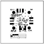


 工商网监
湘ICP备2023018690号
工商网监
湘ICP备2023018690号
