19-0552; Rev 3; 6/08
Overvoltage-Protection Controllers with
Internal FET
Features
The MAX4943–MAX4946/MAX4949 family of overvoltage-protection devices feature a low 80mΩ (typ) RON
internal FET and protect low-voltage systems against
voltage faults up to +28V. These devices also drive an
optional external pFET to protect down to -28V when
connected to a load with reverse current protection.
When the input voltage exceeds the overvoltage threshold, the internal FET is turned off to prevent damage to
the protected components.
♦ Input Voltage Protection Up to +28V
All switches feature a minimum 1.2A current-limit protection. During a short-circuit occurrence, the
MAX4944B and MAX4945B place the switch in a
latchoff state where the switch turns off and remains off.
For the autoretry devices, the switch turns off and continuously checks after a 15ms (typ) retry time.
♦ Low-Current Undervoltage-Lockout Mode
♦ Integrated nFET Switch
♦ Preset Overvoltage Protection Trip Level
7.40V (MAX4943)
6.35V (MAX4944_)
5.80V (MAX4945_)
4.56V (MAX4946)
8.90V (MAX4949)
♦ Short-Circuit Protection (Latchoff/Autoretry)
♦ Internal 15ms (typ) Startup Delay and Retry Times
♦ Input Voltage Power-Good Logic Output
♦ Thermal-Shutdown Protection
The overvoltage thresholds (OVLO) are preset to 7.4V,
6.35V, 5.8V, 4.56V, or 8.9V. The undervoltage-lockout
(UVLO) thresholds are preset to 2.45V and 4.15V.
When the input voltage drops below the undervoltagelockout (UVLO) threshold, the devices enter a lowcurrent standby mode. (See the Ordering Information/
Selector Guide for more details on UVLO/OVLO).
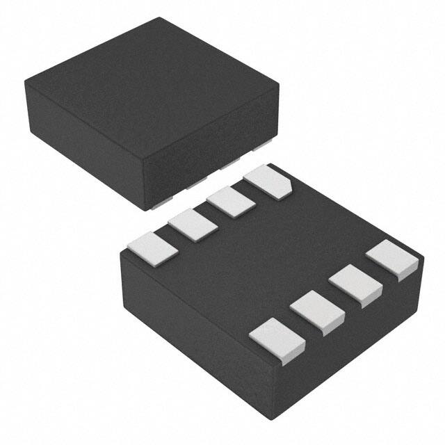
All devices are offered in a small, 8-pin µDFN (2mm x
2mm) package and are specified for operation over the
-40°C to +85°C temperature range.
♦ Small, 8-Pin (2mm x 2mm) µDFN Package
Pin Configuration
TOP VIEW
+
IN 1
IN 2
GP 3
Applications
Cell Phones
PDAs and Palmtop Devices
Digital Still Cameras
MP3 Players
ACOK 4
8 OUT
MAX4943–
MAX4946/
MAX4944L/
MAX4945A/
MAX4945L/
MAX4949
7 OUT
6 OUT
5 GND
µDFN
2mm × 2mm
Ordering Information/Selector Guide
PART
MAX4943ELA+T*
PIN-PACKAGE
TOP MARK
PKG CODE
UVLO (V)
OVLO (V)
OVERCURRENT MODE
8 µDFN
ABA
L822-1
4.15
7.40
Retry
MAX4944ELA+T
8 µDFN
ABB
L822-1
4.15
6.35
Retry
MAX4944BELA+T*
8 µDFN
ABC
L822-1
4.15
6.35
Latchoff
MAX4944LELA+T
8 µDFN
ABD
L822-1
2.45
6.35
Retry
MAX4945ELA+T**
8 µDFN
ABE
L822-1
4.15
5.80
Retry
MAX4945AELA+T**
8 µDFN
ADW
L822-1
4.15
5.80
Retry
MAX4945BELA+T*
8 µDFN
ABF
L822-1
4.15
5.80
Latchoff
MAX4945LELA+T
8 µDFN
ABG
L822-1
2.45
5.80
Retry
MAX4946ELA+T
8 µDFN
ABH
L822-1
2.45
4.56
Retry
MAX4949ELA+T
8 µDFN
ADT
L822-1
2.45
8.90
Latchoff
Note: All devices are specified over the -40°C to +85°C operating temperature range.
+Denotes a lead-free/RoHS-compliant package.
T = Tape-and-reel package.
*Future product—contact factory for availability.
**The OVLO is 6.10V (max) for the MAX4945ELA+T and .6.0V (max) for the MAX4945AELA+T.
________________________________________________________________ Maxim Integrated Products
For pricing, delivery, and ordering information, please contact Maxim Direct at 1-888-629-4642,
or visit Maxim’s website at www.maxim-ic.com.
1
MAX4943–MAX4946/MAX4944L/MAX4945A/MAX4945L/MAX4949
General Description
�MAX4943–MAX4946/MAX4944L/MAX4945A/MAX4945L/MAX4949
Overvoltage-Protection Controllers with
Internal FET
ABSOLUTE MAXIMUM RATINGS
IN ............................................................................-0.3V to +30V
OUT ...............................................................-0.3V to (IN + 0.3V)
GP...........................................................................-0.3V to +12V
IN to GP ..................................................................-0.3V to +22V
ACOK .......................................................................-0.3V to +6V
Continuous Power Dissipation (TA = +70°C)
8-Pin µDFN (derate 4.8mW/°C above +70°C) ..............381mW
Operating Temperature Range ...........................-40°C to +85°C
Junction Temperature ......................................................+150°C
Storage Temperature Range .............................-65°C to +150°C
Lead Temperature (soldering, 10s) .................................+300°C
Stresses beyond those listed under “Absolute Maximum Ratings” may cause permanent damage to the device. These are stress ratings only, and functional
operation of the device at these or any other conditions beyond those indicated in the operational sections of the specifications is not implied. Exposure to
absolute maximum rating conditions for extended periods may affect device reliability.
ELECTRICAL CHARACTERISTICS
(VIN = +5V (MAX4943/MAX4944_/MAX4945_/MAX4949), VIN = +3V (MAX4946), TA = -40°C to +85°C, unless otherwise noted.
Typical values are at TA = +25°C.) (Note 1)
PARAMETER
Input Voltage Range
SYMBOL
Input Supply Current
IIN
UVLO Supply Current
IUVLO
IN Undervoltage Lockout
CONDITIONS
VIN
VUVLO
MIN
VIN = 5V, all remaining parts
50
150
VIN = 2.2V
(VIN falling)
30
MAX4943/MAX4944/
MAX4944B/MAX4945/
MAX4945A/ MAX4945B
3.90
MAX4944L/MAX4945L/
MAX4946/MAX4949
2.30
4.15
VOVLO
(VIN rising)
2.45
2.60
%
MAX4943
7.00
7.4
7.80
MAX4944_
6.00
6.35
6.70
MAX4945/MAX4945B/L
5.50
5.80
6.10
MAX4945A
5.50
5.80
6.00
MAX4946
4.30
4.56
4.82
MAX4949
8.20
8.90
9.60
GP Clamp Voltage
IGPD
GP Pulldown Resistor
RGPD
80
200
VIN = 5V, all remaining parts, IOUT = 1A
80
200
(VIN - VGP), VIN = 28V
TA = +25°C
1.2
1.7
4.0
TA = TMIN to TMAX
1.2
1.7
4.0
TA = +25°C
2.0
3.5
5.0
TA = TMIN to TMAX
2.0
3.0
5.0
16
19
13
50
_______________________________________________________________________________________
V
%
VIN = 3V (MAX4946), IOUT = 1A
ILIM
µA
V
1
RON
µA
4.40
1
MAX4949
2
V
150
MAX4943–MAX4946
Overcurrent Protection Threshold
UNITS
28.0
50
IN Overvoltage Hysteresis
Switch On-Resistance
MAX
VIN = 3V (MAX4946)
IN Undervoltage-Lockout
Hysteresis
Overvoltage Trip Level
TYP
2.2
mΩ
A
V
kΩ
�Overvoltage-Protection Controllers with
Internal FET
(VIN = +5V (MAX4943/MAX4944_/MAX4945_/MAX4949), VIN = +3V (MAX4946), TA = -40°C to +85°C, unless otherwise noted.
Typical values are at TA = +25°C.) (Note 1)
PARAMETER
SYMBOL
ACOK Output-Low Voltage
VOL
CONDITIONS
MIN
TYP
ISINK = 1mA
ACOK High-Leakage Current
V ACOK = 5.5V
Thermal Shutdown
Thermal-Shutdown Hysteresis
MAX
UNITS
0.4
V
1
µA
+175
°C
40
°C
Load Capacitor
300
µF
TIMING CHARACTERISTICS (Figure 2)
tINDBC
Time from VUVLO < VIN < VOVLO to chargepump enable
15
ms
Switch Turn-On Time
tON
VUVLO < VIN < VOVLO, RLOAD = 100Ω,
CLOAD = 300µF, VOUT = from 10% of VOUT
to 80% of VOUT
6
ms
ACOK Assertion Time
t ACOK
VUVLO < VIN < VOVLO, to ACOK low
30
ms
Switch Turn-Off Time
tOFF
VIN < VUVLO or VIN > VOVLO, to internal
switch off
2
Overcurrent fault to internal switch turn-off
10
µs
From overcurrent fault to internal switch
turn-on
15
ms
Debounce Time
Autoretry Time
tRETRY
20
µs
Note 1: All specifications are 100% production tested at TA = +25°C, unless otherwise noted. Specifications are over -40°C to +85°C
and are guaranteed by design.
Typical Operating Characteristics
(TA = +25°C, unless otherwise noted.)
SUPPLY CURRENT
vs. SUPPLY VOLTAGE
100
210
RON (mΩ)
180
150
120
90
80
60
40
60
20
30
2
6
10
14
18
SUPPLY VOLTAGE (V)
22
26
1.008
1.006
1.004
1.002
1.000
0.998
0.996
0.994
0.992
0
0
MAX4943 toc03
120
1.010
NORMALIZED UVLO THRESHOLD
MAX4943 toc02
MAX4944
240
SUPPLY CURRENT (nA)
140
MAX4943 toc01
300
270
NORMALIZED UVLO THRESHOLD
vs. TEMPERATURE
RON
vs. TEMPERATURE
0.990
-40
-15
10
35
TEMPERATURE (°C)
60
85
-40
-15
10
35
60
85
TEMPERATURE (°C)
_______________________________________________________________________________________
3
MAX4943–MAX4946/MAX4944L/MAX4945A/MAX4945L/MAX4949
ELECTRICAL CHARACTERISTICS (continued)
�Typical Operating Characteristics (continued)
(TA = +25°C, unless otherwise noted.)
1.004
1.002
1.000
0.998
0.996
36
34
MAX4943 toc06
38
23
21
19
17
32
0.994
25
DEBOUNCE TIME (ms)
1.006
40
MAX4943 toc05
1.008
ACOK ASSERTION TIME (ms)
MAX4943 toc04
1.010
DEBOUNCE TIME
vs. TEMPERATURE
ACOK ASSERTION TIME
vs. TEMPERATURE
NORMALIZED OVLO THRESHOLD
vs. TEMPERATURE
NORMALIZED OVLO THRESHOLD
MAX4943–MAX4946/MAX4944L/MAX4945A/MAX4945L/MAX4949
Overvoltage-Protection Controllers with
Internal FET
0.992
15
30
0.990
-40
-15
10
35
60
-40
85
-15
10
35
60
85
-40
POWER-UP RESPONSE
-15
10
35
TEMPERATURE (°C)
TEMPERATURE (°C)
TEMPERATURE (°C)
UNDERVOLTAGE FAULT RESPONSE
MAX4943 toc07
MAX4943 toc08
5V
ADAPTER
5V/div
3V ADAPTER
2V/div
5V
VIN
5V/div
VIN
3V 2V/div
VOUT
5V/div
VOUT
0 5V/div
VACOK
5V/div
0
IOUT
2A/div
10ms/div
IOUT
0 1A/div
4μs/div
OVERCURRENT DURATION TIME
(DURING AUTORETRY)
SHORT-CIRCUIT FAULT RESPONSE
MAX4943 toc09
MAX4943 toc10
RLOAD = 1Ω
COUT = 0.1μF
ADAPTER
2V/div
VOUT
1V/div
VIN
5V/div
VOUT
5V/div
VACOK
5V/div
CIN = 1000μF
1μs/div
4
VACOK
5V/div
IOUT
1A/div
IOUT
10A/div
10μs/div
_______________________________________________________________________________________
60
85
�Overvoltage-Protection Controllers with
Internal FET
PIN
NAME
FUNCTION
1, 2
IN
Voltage Input. IN powers the charge pump required to turn on the internal switch. When the correct
adapter is plugged in, a 15ms (typ) debouncer prevents false turn-on of the internal switch. Bypass
IN to GND with a 1µF ceramic capacitor as close as possible to the device to enable ±15kV (HBM)
ESD protection on IN.
3
GP
pFET Gate-Drive Output. GP pulls the external pFET gate down when the input is above ground.
4
ACOK
5
GND
Ground
6, 7, 8
OUT
Output Voltage. Output of internal switch. Short all pins together for proper operation.
Active-Low Open-Drain Adapter-Voltage Indicator Output. ACOK is driven low after the adapter
voltage is stable between VUVLO and VOVLO for 30ms (typ). Connect a pullup resistor from ACOK to
the logic I/O voltage of the host system.
OUT
IN
CHARGE
PUMP
GP
CHARGE-PUMP
ENABLED
GND
15ms (typ)
DEBOUNCE
TIMER AND
RETRY TIME
+
VOVLO
-
RESET
OVERCURRENT
OR
THERMAL
FAULTS
OSCILLATOR
VUVLO
+
-
RESET
30ms (typ)
TIMER
ACOK
MAX4943–MAX4946/MAX4944L/
MAX4945L/MAX4949
Figure 1. Functional Diagram
Detailed Description
The MAX4943–MAX4946/MAX4949 overvoltage-protection devices feature a low RON internal FET and protect
low-voltage systems against voltage faults up to +28V. If
the input voltage exceeds the overvoltage threshold, the
internal MOSFET is turned off to prevent damage to the
protected components. These devices also drive an
optional external pFET to protect down to -28V. If the
adapter voltage drops below ground, the pFET turns off
to prevent damage to the protected components due to
negative voltage exposure. The internal charge pump’s
15ms (typ) debounce time prevents false turn-on of the
internal switch during startup. An open-drain, active-low
logic output is available to signal that a successful
power-up has occurred.
_______________________________________________________________________________________
5
MAX4943–MAX4946/MAX4944L/MAX4945A/MAX4945L/MAX4949
Pin Description
�MAX4943–MAX4946/MAX4944L/MAX4945A/MAX4945L/MAX4949
Overvoltage-Protection Controllers with
Internal FET
OVLO
UVLO
tOFF
IN
tOFF
tON
80% VIN
10% VIN
OUT
tINDBC
tINDBC
tACOK
tINDBC
tACOK
ACOK
Figure 2. Timing Diagram
Device Operation
The MAX4943–MAX4946/MAX4949 have an internal
oscillator and charge pump that control the turn-on
of the internal switch. The internal oscillator controls
the timers that enable the turn-on of the charge pump
and controls the state of the open-drain ACOK
output. If VIN < VUVLO or if VIN >VOVLO, the internal
oscillator remains off, thus disabling the charge pump.
If VUVLO < VIN < VOVLO, the internal charge pump is
enabled. The charge-pump startup, after a 15ms (typ)
internal delay, turns on the internal switch (see Figure 2).
ACOK is held high during startup until the ACOK 30ms
(typ) blanking period expires. At this point, the device is
in its on state.
At any time, if VIN drops below VUVLO or rises above
V OVLO, ACOK is pulled high and the charge pump
is disabled.
Internal Switch
The MAX4943–MAX4946/MAX4949 incorporate an
internal nFET with a 80mΩ (typ) RON. The switch is
internally driven by a charge pump that generates a 5V
6
voltage above the input voltage. The internal switch is
equipped with 1.2A (min) current-limit protection that
turns off the switch within 10µs (typ) during an overcurrent fault condition.
Autoretry
The MAX4943–MAX4946 have an overcurrent autoretry
function that turns on the switch again after a 15ms (typ)
retry time (see Figure 3). If the faulty load condition is still
present after the blanking time, the switch turns off again
and the cycle is repeated. The fast turn-off time and
15ms retry time result in a very low duty cycle to keep
power consumption low. If the faulty load condition is not
present, the switch remains on.
Latch
The MAX4944B/MAX4945B/MAX4949 do not have the
autoretry function, and the switch latches off after an
overcurrent fault. The switch remains off until the overcurrent fault has been removed. The switch turns back
on when the adapter voltage goes below VUVLO and
then returns to the valid operating range.
_______________________________________________________________________________________
�Overvoltage-Protection Controllers with
Internal FET
tOFF
SWITCH ON
SWITCH ON
Undervoltage Lockout (UVLO)
The MAX4944L/MAX4945L/MAX4946/MAX4949 have a
2.45V (typ) undervoltage-lockout threshold (VUVLO),
while the remaining devices have a 4.15V (typ) VUVLO
threshold. When VIN is less than VUVLO, ACOK is high
impedance.
Overvoltage-Lockout Thresholds (OVLO)
The MAX4943 has a 7.4V (typ) overvoltage threshold
(V OVLO ), the MAX4944_ has a 6.35V (typ) V OVLO
threshold, the MAX4945_ has a 5.80V (typ) V OVLO
threshold, the MAX4946 has a 4.56V (typ) V OVLO
threshold, and the MAX4949 has a 8.90V (typ) VOVLO
threshold. When VIN is greater than OVLO, ACOK is
high impedance.
tRETRY
CURRENT
THROUGH
SWITCH
SWITCH OFF
ILIM
Figure 3. Autoretry Timing Diagram
ACOK
ACOK is an active-low, open-drain output that asserts
low when VUVLO < VIN < VOVLO for the 30ms (typ) period. Connect a pullup resistor from ACOK to the logic
I/O voltage of the host system. During a short-circuit
fault, ACOK may deassert due to VIN not being in the
valid operating voltage range.
Thermal-Shutdown Protection
The MAX4943–MAX4946/MAX4949 feature thermal-shutdown circuitry. The internal switch turns off when the junction temperature exceeds +175°C (typ) and immediately
goes into a fault mode. The device exits thermal shutdown after the junction temperature cools by 40°C (typ).
Applications Information
RC
1MΩ
CHARGE-CURRENTLIMIT RESISTOR
HIGHVOLTAGE
DC
SOURCE
Cs
100pF
RD
1.5kΩ
DISCHARGE
RESISTANCE
DEVICE
UNDER
TEST
STORAGE
CAPACITOR
Figure 4. Human Body ESD Test Model
IN Bypass Capacitor
For most applications, bypass IN to GND with a 1µF
ceramic capacitor as close as possible to the device to
enable ±15kV (HBM) ESD protection on the pin. If
±15kV is not required, there is no capacitor required at
IN. If the power source has significant inductance due
to long lead length, take care to prevent overshoots
due to the LC tank circuit and provide protection if necessary to prevent exceeding the +30V absolute maximum rating on IN.
Reverse Polarity Protection
The optional external pFET can provide reverse polarity
protection down to -28V (for a 30V pFET), if the protect-
IP 100%
90%
Ir
PEAK-TO-PEAK RINGING
(NOT DRAWN TO SCALE)
AMPERES
36.8%
10%
0
0
tRL
TIME
tDL
CURRENT WAVEFORM
Figure 5. Human Body Current Waveform
_______________________________________________________________________________________
7
MAX4943–MAX4946/MAX4944L/MAX4945A/MAX4945L/MAX4949
GP GATE Drive
When the input voltage goes above ground, GP pulls
low and turns on the pFET. An internal clamp protects
the pFET by ensuring that the GP to IN voltage does not
exceed 19V (max) when the input (IN) rises to +28V.
�MAX4943–MAX4946/MAX4944L/MAX4945A/MAX4945L/MAX4949
Overvoltage-Protection Controllers with
Internal FET
ed device does not allow current to flow into OUT. The
pFET is turned off when the voltage between GP and IN
is less than the pFET gate threshold voltage.
RC
50MΩ TO 100MΩ
ESD Test Conditions
CHARGE-CURRENTLIMIT RESISTOR
ESD performance depends on a number of conditions.
The MAX4943–MAX4946/MAX4949 are specified for
±15kV (HBM) typical ESD resistance on IN when IN is
bypassed to ground with a 1µF ceramic capacitor.
HIGHVOLTAGE
DC
SOURCE
Cs
150pF
RD
330Ω
DISCHARGE
RESISTANCE
STORAGE
CAPACITOR
DEVICE
UNDER
TEST
Human Body Model
Figure 4 shows the Human Body Model and Figure 5
shows the current waveform it generates when discharged into a low impedance. This model consists of a
100pF capacitor charged to the ESD voltage of interest,
which is then discharged into the device through a
1.5kΩ resistor.
IEC 61000-4-2
The IEC 61000-4-2 standard covers ESD testing and
performance of finished equipment. It does not specifically refer to integrated circuits. The MAX4943–
MAX4946/MAX4949 are specified for ±15kV Air-Gap
Discharge and ±8kV Contact Discharge IEC 61000-4-2
on the IN pin when IN is bypassed to ground with a 1µF
ceramic capacitor.
The major difference between tests done using the
Human Body Model and IEC 61000-4-2 is a higher peak
current in IEC 61000-4-2, due to lower series resistance.
Figure 6. IEC 61000-4-2 ESD Test Model
Hence, the ESD withstand voltage measured to IEC
61000-4-2 generally is lower than that measured using the
Human Body Model. Figure 6 shows the IEC 61000-4-2
model. The Contact Discharge method connects the
probe to the device before the probe is charged. The
Air-Gap Discharge test involves approaching the device
with a charged probe.
Chip Information
PROCESS: BiCMOS
Typical Operating Circuit
5V AC
ADAPTER
1μF
GP
IN
VI/0
TO μC
OUT
15ms (typ)
DEBOUNCE
ACOK
30ms (typ)
TIMER
GND
8
CHARGE
PUMP
CHARGER
DC-DC
CONVERTER
MAX4943–MAX4946/MAX4944L/
MAX4945L/MAX4949
_______________________________________________________________________________________
�Overvoltage-Protection Controllers with
Internal FET
PACKAGE TYPE
PACKAGE CODE
DOCUMENT NO.
8 µDFN
L822-1
21-0164
_______________________________________________________________________________________
9
MAX4943–MAX4946/MAX4944L/MAX4945A/MAX4945L/MAX4949
Package Information
For the latest package outline information and land patterns, go to www.maxim-ic.com/packages.
�MAX4943–MAX4946/MAX4944L/MAX4945A/MAX4945L/MAX4949
Overvoltage-Protection Controllers with
Internal FET
Revision History
REVISION
NUMBER
REVISION
DATE
2
7/07
—
3
6/08
Added MAX4945A to the Ordering Information/Selector Guide and Electrical
Characterstics tables
DESCRIPTION
PAGES
CHANGED
1, 2, 3
1, 2
Maxim cannot assume responsibility for use of any circuitry other than circuitry entirely embodied in a Maxim product. No circuit patent licenses are
implied. Maxim reserves the right to change the circuitry and specifications without notice at any time.
10 ____________________Maxim Integrated Products, 120 San Gabriel Drive, Sunnyvale, CA 94086 408-737-7600
© 2008 Maxim Integrated Products
is a registered trademark of Maxim Integrated Products, Inc.
�


 工商网监
湘ICP备2023018690号
工商网监
湘ICP备2023018690号
