19-0291; Rev 2; 2/10
Hex/Quad, Power-Supply Supervisory Circuits
The MAX6887/MAX6888 multivoltage supply supervisors provide several voltage-detector inputs, one watchdog input, and three outputs. Each voltage-detector
input offers a factory-set undervoltage and overvoltage
threshold. Manual reset and margin disable inputs offer
additional flexibility.
The MAX6887 offers six voltage-detector inputs, while
the MAX6888 offers four inputs. Output RESET asserts
when any input voltage drops below its respective
undervoltage threshold or manual reset MR is asserted.
Output OV asserts when any input voltage exceeds its
respective overvoltage threshold. Monitor standard
supply voltages listed in the Selector Guide.
The MAX6887/MAX6888 offer a watchdog timer with an
initial and normal timeout periods of 102.4s and 1.6s,
respectively. Watchdog output WDO asserts when the
watchdog timer expires. Connect WDO to manual reset
input MR to generate resets when the watchdog timer
expires. RESET, OV, and WDO are active-low, opendrain outputs.
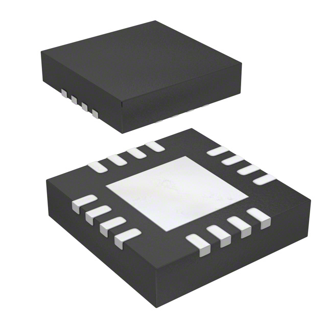
The MAX6887/MAX6888 are available in a 5mm x 5mm
x 0.8mm, 16-pin thin QFN package and operate over
the extended -40°C to +85°C temperature range.
Applications
Features
o Hex/Quad Voltage Detectors
o Undervoltage and Overvoltage Thresholds
o 1% Threshold Accuracy
o Margining Disable and Manual Reset Input
o Watchdog Timer
o Open-Drain RESET, OV, and WDO Outputs
o 180ms (min) Reset Timeout Period
o Few External Components
o Small 5mm x 5mm, 16-Pin Thin QFN Packages
Ordering Information
PART
TEMP RANGE
PIN-PACKAGE
MAX6887_ETE+
-40°C to +85°C
16 Thin QFN-EP*
MAX6888_ETE+
-40°C to +85°C
16 Thin QFN-EP*
Note: Insert the desired letter from the Selector Guide into the
blank to complete the part number.
+Denotes a lead(Pb)-free/RoHS-compliant package.
*EP = Exposed pad.
Multivoltage Systems
Telecom
Networking
Servers/Workstations/Storage Systems
Pin Configurations and Typical Operating Circuit appear at
end of data sheet.
Selector Guide
PART
NOMINAL INPUT VOLTAGE (V)*
NOMINAL INPUT VOLTAGE (V)*
IN4
IN5
IN6
TOL
(%)
2.5
1.8
Adj
Adj
5
MAX6887IETE
5.0
3.3
2.5
1.8
Adj
Adj
10
2.5
Adj
Adj
Adj
5
MAX6887JETE
5.0
3.3
2.5
Adj
Adj
Adj
10
3.3
1.8
Adj
Adj
Adj
5
MAX6887KETE
5.0
3.3
1.8
Adj
Adj
Adj
10
2.5
1.8
1.5
Adj
Adj
5
MAX6887LETE
3.3
2.5
1.8
1.5
Adj
Adj
10
3.3
2.5
1.8
Adj
Adj
Adj
5
MAX6887METE 3.3
2.5
1.8
Adj
Adj
Adj
10
3.3
2.5
1.5
Adj
Adj
Adj
5
MAX6887NETE 3.3
2.5
1.5
Adj
Adj
Adj
10
IN1
IN2
IN3
MAX6887AETE
5.0
3.3
MAX6887BETE
5.0
3.3
MAX6887CETE 5.0
MAX6887DETE 3.3
MAX6887EETE
MAX6887FETE
PART
IN1
IN2
IN3
IN4
IN5
IN6
TOL
(%)
MAX6887GETE 3.3
2.5
Adj
Adj
Adj
Adj
5
MAX6887OETE 3.3
2.5
Adj
Adj
Adj
Adj
10
MAX6887HETE 3.3
1.8
Adj
Adj
Adj
Adj
5
MAX6887PETE
3.3
1.8
Adj
Adj
Adj
Adj
10
MAX6887QETE
Adj
Adj
Adj
Adj
Adj
5
MAX6887RETE
Adj
Adj
Adj
Adj
Adj
Adj
10
Adj
*See thresholds options tables (Tables 1 and 2) for actual undervoltage and overvoltage thresholds.
Selector Guides continued at end of data sheet.
________________________________________________________________ Maxim Integrated Products
1
For pricing, delivery, and ordering information, please contact Maxim Direct at 1-888-629-4642,
or visit Maxim’s website at www.maxim-ic.com.
MAX6887/MAX6888
General Description
�MAX6887/MAX6888
Hex/Quad, Power-Supply Supervisory Circuits
ABSOLUTE MAXIMUM RATINGS
(All voltages referenced to GND.)
IN1–IN6, VCC, RESET, OV, WDO .............................-0.3V to +6V
WDI, MR, MARGIN ...................................................-0.3V to +6V
BP .............................................................................-0.3V to +3V
Input/Output Current (all pins)..........................................±20mA
Continuous Power Dissipation (TA = +70°C)
16-Pin 5mm x 5mm Thin QFN
(derate 20.8mW/°C above +70°C) ..............................1667mW
Maximum Junction Temperature .....................................+150°C
Operating Temperature Range ...........................-40°C to +85°C
Storage Temperature Range .............................-65°C to +150°C
Lead Temperature (soldering, 10s) .................................+300°C
Stresses beyond those listed under “Absolute Maximum Ratings” may cause permanent damage to the device. These are stress ratings only, and functional
operation of the device at these or any other conditions beyond those indicated in the operational sections of the specifications is not implied. Exposure to
absolute maximum rating conditions for extended periods may affect device reliability.
ELECTRICAL CHARACTERISTICS
(VIN1–VIN4 or VCC = 2.7V to 5.8V, WDI = GND, MARGIN = MR = BP, TA = -40°C to +85°C, unless otherwise noted. Typical values are
at TA = +25°C.) (Notes 1, 2)
PARAMETER
SYMBOL
Operating Voltage Range
(Note 3)
Voltage on either one of IN1–IN4 or VCC to
guarantee the part is fully operational
Supply Current
ICC
Threshold Accuracy
(See the Selector Guide)
VTH
Threshold Hysteresis
VTH-HYST
Threshold Tempco
∆VTH/°C
IN_ Input Impedance
RIN
IN_ Input Leakage Current
IIN
Power-Up Delay
CONDITIONS
tD-PO
TYP
2.7
VIN1 = 5.8V, IN2–IN6 = GND, no load
0.9
MAX
UNITS
5.8
V
1.2
mA
IN1–IN6, IN_ falling, TA = +25°C to +85°C
-1
+1
IN1–IN6, IN_ falling, TA = -40°C to +85°C
-1.5
+1.5
For VIN_ < highest VIN1–IN4 and
VIN_ < VCC (not ADJ), thresholds are not set
as adjustable
IN5, IN6 (MAX6887 only)
IN1–IN4 set as adjustable thresholds
130
tD-R
% VTH
10
ppm/°C
200
-150
RESET Timeout Period
tRP
OV Timeout Period
tOP
RESET, OV, and WDO Output
Low
VOL
ISINK = 4mA, output asserted
RESET, OV, and WDO Output
Open-Drain Leakage Current
ILKG
Output high impedance
IN_ falling/rising, 100mV overdrive
300
kΩ
+150
nA
2.5
ms
220
ms
20
180
% VTH
0.3
VCC ≥ 2.5V
IN_ to RESET or OV Delay
2
MIN
200
µs
25
-1
_______________________________________________________________________________________
µs
0.4
V
+1
µA
�Hex/Quad, Power-Supply Supervisory Circuits
(VIN1–VIN4 or VCC = 2.7V to 5.8V, WDI = GND, MARGIN = MR = BP, TA = -40°C to +85°C, unless otherwise noted. Typical values are
at TA = +25°C.) (Notes 1, 2)
PARAMETER
SYMBOL
CONDITIONS
MIN
TYP
VIL
MR, MARGIN, WDI Input Voltage
MR Input Pulse Width
UNITS
0.6
VIH
1.4
tMR
1
V
µs
MR Glitch Rejection
100
MR to RESET or OV Delay
tD-MR
MR to Internal BP Pullup Current
IMARGIN
WDI Pulldown Current
ns
200
IMR
MARGIN to Internal BP Pullup
Current
IWDI
ns
VMR = 1.4V
5
10
15
µA
VMARGIN = 1.4V
5
10
15
µA
5
10
15
µA
VWDI = 0.6V
WDI Input Pulse Width
50
Watchdog Timeout Period
Note 1:
Note 2:
Note 3:
Note 4:
MAX
ns
tWDI
Initial
92.16
102.4
112.64
tWD
Normal
1.44
1.6
1.76
s
100% production tested at TA = +25°C and TA = +85°C. Specifications at TA = -40°C are guaranteed by design.
Device may be supplied from any one of IN1–IN4 or VCC.
The internal supply voltage, measured at VCC, equals the maximum of IN1–IN4.
Versions Q and R require that power be applied through VCC.
Typical Operating Characteristics
(VIN1–VIN4 or VCC = 5V, WDI = GND, MARGIN = MR = BP, TA = +25°C, unless otherwise noted.)
IN1–IN4 SUPPLY CURRENT
vs. IN1–IN4 SUPPLY VOLTAGE
0.85
0.80
TA = +25°C
TA = -40°C
0.75
TA = +85°C
0.90
0.85
0.80
TA = +25°C
0.70
3.6
4.6
SUPPLY VOLTAGE (V)
5.6
210
205
200
195
185
0.70
2.6
215
190
TA = -40°C
0.75
MAX6887 toc03
0.95
TIMEOUT PERIOD (ms)
0.90
220
MAX6887 toc02
TA = +85°C
SUPPLY CURRENT (mA)
SUPPLY CURRENT (mA)
0.95
1.00
MAX6887 toc01
1.00
RESET TIMEOUT PERIOD
vs. TEMPERATURE
VCC SUPPLY CURRENT
vs. VCC SUPPLY VOLTAGE
180
2.6
3.6
4.6
SUPPLY VOLTAGE (V)
5.6
-40
-15
10
35
60
85
TEMPERATURE (°C)
_______________________________________________________________________________________
3
MAX6887/MAX6888
ELECTRICAL CHARACTERISTICS (continued)
�Typical Operating Characteristics (continued)
(VIN1–VIN4 or VCC = 5V, WDI = GND, MARGIN = MR = BP, TA = +25°C, unless otherwise noted.)
27
26
25
24
23
1.650
1.625
1.600
1.575
1.550
22
21
1.525
20
1.500
-40
-15
10
35
60
85
1.005
MAX6887 toc06
1.675
TIMEOUT PERIOD (s)
1.004
1.003
1.002
1.001
1.000
0.999
0.998
0.997
0.996
0.995
-40
-15
10
35
60
-40
85
-15
10
35
60
85
TEMPERATURE (°C)
TEMPERATURE (°C)
TEMPERATURE (°C)
MAXIMUM IN_ TRANSIENT
vs. IN_THRESHOLD OVERDRIVE
OUTPUT-VOLTAGE LOW vs. SINK CURRENT
MR TO RESET OUTPUT PROPAGATION
DELAY vs. TEMPERATURE
150
125
100
PO_ ASSERTION OCCURS
ABOVE THIS LINE
75
50
300
250
200
150
100
50
0
0
1
10
100
1000
IN_ THRESHOLD OVERDRIVE (mV)
MAX6887 toc09
350
25
3.00
MAX8667 toc08
175
400
OUTPUT-VOLTAGE LOW (mV)
MAX6887 toc07
200
2.75
PROPAGATION DELAY (µs)
PROPAGATION DELAY (µs)
28
MAX6887 toc05
100mV OVERDRIVE
29
1.700
MAX6887 toc04
30
NORMALIZED IN_ THRESHOLD
vs. TEMPERATURE
WATCHDOG TIMEOUT PERIOD
vs. TEMPERATURE
NORMALIZED IN_ THRESHOLD
IN_ TO RESET OR OV
PROPAGATION DELAY vs. TEMPERATURE
MAXIMUM TRANSIENT DURATION (µs)
MAX6887/MAX6888
Hex/Quad, Power-Supply Supervisory Circuits
2.50
2.25
2.00
1.75
1.50
1.25
1.00
0
2
4
6
8
10
12
14
SINK CURRENT (mA)
-40
-15
10
35
60
85
TEMPERATURE (°C)
Pin Description
PIN
NAME
MAX6887
MAX6888
1
1
RESET
2
2
WDO
3
3
OV
4
4
GND
4
FUNCTION
Open-Drain, Active-Low Reset Output. RESET asserts when any input voltage falls below its
undervoltage threshold or when MR is pulled low. RESET remains low for 200ms after all
assertion-causing conditions are cleared. An external pullup resister is required.
Open-Drain, Active-Low Watchdog Timer Output. Logic output for the watchdog timer function.
WDO goes low when WDI is not strobed high-to-low or low-to-high within the watchdog timeout
period.
Open-Drain Active-Low Overvoltage Output. OV asserts when any input voltage exceeds its
overvoltage threshold. OV remains low for 25µs after all overvoltage conditions are cleared.
An external pullup resistor is required.
Ground
_______________________________________________________________________________________
�Hex/Quad, Power-Supply Supervisory Circuits
PIN
MAX6887
MAX6888
5
5
NAME
FUNCTION
MR
Manual Reset Input. Pull MR low to assert RESET. Connect MR to WDO to generate resets
when the watchdog timer expires. Leave MR unconnected or connect to DBP if unused. MR is
internally pulled up to BP through a 10µA current source.
6
6
MARGIN
Margin Input. When MARGIN is pulled low, RESET is held in its existing state independent of
subsequent changes in monitored input voltages or the watchdog timer expiration. MARGIN is
internally pulled up to BP through a 10µA current source. Leave MARGIN unconnected or
connect to BP if unused. MARGIN overrides MR if both are asserted at the same time.
7
7
WDI
Watchdog Timer Input. Logic input for the watchdog timer function. If WDI is not strobed with a
valid low-to-high or high-to-low transition within the selected watchdog timeout period, WDO
asserts. WDI is internally pulled down to GND through a 10µA current sink.
8
8
I.C.
Internal Connection. Leave unconnected.
9
9
VCC
Internal Power-Supply Voltage. Bypass VCC to GND with a 1µF ceramic capacitor as close to
the device as possible. VCC supplies power to the internal circuitry. VCC is internally powered
from the highest of the monitored IN1–IN4 voltages. Do not use VCC to supply power to external
circuitry. To externally supply VCC, see the Powering the MAX6887/MAX6888 section.
10
10
BP
Bypass Voltage. The internally generated voltage at BP supplies power to internal logic and
output RESET. Connect a 1µF capacitor from BP to GND as close to the device as possible. Do
not use BP to supply power to external circuitry.
IN6
Input Voltage Detector 6. IN6 monitors both undervoltage and overvoltage conditions. See the
thresholds options (Tables 1 and 2) for available thresholds. IN6 cannot power the device. For
improved noise immunity, bypass IN6 to GND with a 0.1µF capacitor installed as close to the
device as possible.
IN5
Input Voltage Detector 5. IN5 monitors both undervoltage and overvoltage conditions. See the
thresholds options (Tables 1 and 2) for available thresholds. IN5 cannot power the device. For
improved noise immunity, bypass IN5 to GND with a 0.1µF capacitor installed as close to the
device as possible.
IN4
Input Voltage Detector 4. IN4 monitors both undervoltage and overvoltage conditions. See the
thresholds options (Tables 1 and 2) for available thresholds. Power the device through IN1–IN4
or VCC (see the Powering the MAX6887/MAX6888 section). For improved noise immunity,
bypass IN4 to GND with a 0.1µF capacitor installed as close to the device as possible.
IN3
Input Voltage Detector 3. IN3 monitors both undervoltage and overvoltage conditions. See the
thresholds options (Tables 1 and 2) for available thresholds. Power the device through IN1–IN4
or VCC (see the Powering the MAX6887/MAX6888 section). For improved noise immunity,
bypass IN3 to GND with a 0.1µF capacitor installed as close to the device as possible.
IN2
Input Voltage Detector 2. IN2 monitors both undervoltage and overvoltage conditions. See the
thresholds options (Tables 1 and 2) for available thresholds. Power the device through IN1–IN4
or VCC (see the Powering the MAX6887/MAX6888 section). For improved noise immunity,
bypass IN2 to GND with a 0.1µF capacitor installed as close to the device as possible.
11
12
13
14
15
—
—
13
14
15
16
16
IN1
Input Voltage Detector 1. IN1 monitors both undervoltage and overvoltage conditions. See the
thresholds options (Tables 1 and 2) for available thresholds. Power the device through IN1–IN4
or VCC (see the Powering the MAX6887/MAX6888 section). For improved noise immunity,
bypass IN1 to GND with a 0.1µF capacitor installed as close to the device as possible.
—
11, 12
N.C.
No Connection. Not internally connected.
—
—
EP
Exposed Paddle. Internally connected to GND. Connect EP to GND or leave unconnected.
_______________________________________________________________________________________
5
MAX6887/MAX6888
Pin Description (continued)
�Hex/Quad, Power-Supply Supervisory Circuits
MAX6887/MAX6888
Functional Diagram
WDI
*IN_
DETECTOR
IN1
MARGIN
MR
IN2
IN2 DETECTOR
IN3
IN3 DETECTOR
IN4
IN4 DETECTOR
IN5
(N.C.)
IN6
(N.C.)
IN5 DETECTOR
RESET TIMING BLOCK
OV
OV TIMING BLOCK
(VIRTUAL DIODES)
IN6 DETECTOR
LOGIC ARRAY
RESET
WDO
WDO TIMING BLOCK
VCC
REFERENCE
1µF
2.55V
LDO
MAX6887
MAX6888
BP
1µF
( ) MAX6888 ONLY
GND
*FOR ADJUSTABLE INPUTS REFER TO THE ADJUSTABLE THRESHOLD INPUTS SECTION.
6
_______________________________________________________________________________________
�Hex/Quad, Power-Supply Supervisory Circuits
The MAX6887/MAX6888 provide several supply-detector
inputs, one watchdog input, and three outputs for powersupply monitoring applications. The MAX6887 offers six
voltage-detector inputs, while the MAX6888 offers four.
Each voltage-detector input offers both an undervoltage
and overvoltage threshold.
The undervoltage and overvoltage thresholds are factory-set for monitoring standard supply voltages (see the
Selector Guide). Inputs in the Selector Guide that contain “Adj” allow an external voltage-divider to be connected to set a user-defined threshold.
RESET goes low when any input voltage drops below
its undervoltage threshold or when MR is brought low.
RESET stays low for 200ms after all assertion-causing
conditions have been cleared. OV goes low when an
input voltage rises above its overvoltage threshold. OV
typically stays low for 25µs (typ) after all inputs fall
back under their overvoltage thresholds.
The MAX6887/MAX6888 offer a watchdog timer with
initial and normal timeout periods of 102.4s and 1.6s,
respectively. WDO goes low when the watchdog timer
expires and deasserts when WDI transitions from lowto-high or high-to-low.
The MAX6887/MAX6888 generate a supply voltage at
BP for the internal logic circuitry. Bypass BP to GND with
a 1µF ceramic capacitor installed as close to the device
as possible. The nominal BP output voltage is +2.55V.
Do not use BP to provide power to external circuitry.
Inputs
The MAX6887 offers six voltage-detector inputs, while
the MAX6888 offers four voltage-detector inputs. Each
voltage-detector input offers an undervoltage and overvoltage threshold set at the factory to monitor standard
supply voltages (see the Selector Guide). The 5% and
10% tolerances are based on maximum and minimum
threshold values. Actual thresholds for the
MAX6887/MAX6888 are shown in Tables 1 and 2.
Inputs in the Selector Guide listing “Adj” allow an external voltage-divider to be connected to set a userdefined threshold.
Adjustable Threshold Inputs
Inputs listed in the Selector Guide containing “Adj” for
inputs allow external resistor voltage-dividers to be
connected at the voltage-detector inputs. These inputs
monitor any voltage supply higher than 0.6V (see
Figure 1). Use the following equation to set a voltage-
Powering the MAX6887/MAX6888
The MAX6887/MAX6888 derive power from the voltagedetector inputs IN1–IN4 or through an externally supplied VCC. A virtual diode-ORing scheme selects the
positive input that supplies power to the device (see
the Functional Diagram). The highest input voltage on
IN1–IN4 supplies power to the device. One of IN1–IN4
must be at least 2.7V to ensure proper operation.
Internal hysteresis ensures that the supply input that
initially powered the device continues to power the
device when multiple input voltages are within 50mV of
each other.
VCC powers the analog circuitry and is the bypass connection for the MAX6887/MAX6888 internal supply.
Bypass V CC to GND with a 1µF ceramic capacitor
installed as close to the device as possible. The internal supply voltage, measured at VCC, equals the maximum of IN1–IN4. If VCC is externally supplied, VCC
must be at least 200mV higher than any voltage
applied to IN1–IN4 and VCC must be brought up first.
VCC always powers the device when all IN_ are factory
set as “Adj.” Do not use the internally generated VCC to
provide power to external circuitry.
VIN
MAX6887
MAX6888
R1
IN_
R2
*VREFUV
*VREFOV
*VREFOV AND VREFUV ARE REFERENCED
TO 0.6V ACCORDING TO THE DEVICE'S TOLERANCE
Figure 1. Adjusting the Monitored Threshold
_______________________________________________________________________________________
7
MAX6887/MAX6888
Detailed Description
�MAX6887/MAX6888
Hex/Quad, Power-Supply Supervisory Circuits
detector input (IN1–IN6) to monitor a user-defined supply voltage:
⎛ R2 ⎞
0.6V = VMON × ⎜
⎟
⎝ R1+ R2 ⎠
where VMON is the desired voltage to be monitored.
Use the following procedure to design the proper voltage-divider and calculate thresholds:
1) Pick a value for R2. Use the equation above with
the desired supply voltage to be monitored and
solve for R1. Use high-value resistors R1 and R2 to
minimize current consumption due to low leakage
currents.
2) To find the actual undervoltage and overvoltage
thresholds, use the following equations:
⎛V
⎞
VACTUALUV = VMON × ⎜ REFUV ⎟
⎝ 0.6V ⎠
⎛V
⎞
VACTUALOV = VMON × ⎜ REFOV ⎟
⎝ 0.6V ⎠
VREFUV and VREFOV are the undervoltage and overvoltage thresholds listed in Tables 1 and 2 that allow
adjustable thresholds. Their values are based on tolerances of ±7.5% and ±12.5% from a 0.6V reference.
See the Selector Guide to find which thresholds in
Tables 1 and 2 are adjustable.
Manual Reset (MR)
Many µP-based products require manual reset capability
to allow an operator or external logic circuitry to initiate a
reset. The manual reset input (MR) can be connected
directly to a switch without an external pullup resistor or
debouncing network. MR is internally pulled up to BP.
Leave unconnected if not used. MR is internally pulled
up to BP through a 10µA current source. MR is designed
to reject fast, falling transients (typically 100ns pulses)
and MR must be held low for a minimum of 1µs to assert
RESET. Connect a 0.1µF capacitor from MR to ground to
provide additional noise immunity. After MR transitions
from low to high, RESET remains asserted for the duration of its time delay.
Margin Output Disable (MARGIN)
MARGIN allows system-level testing while power supplies exceed the normal operating ranges. Drive
MARGIN low to hold RESET, OV, and WDO in their
Table 1. MAX6887 Threshold Options
PART
UV THRESHOLDS (V)
OV THRESHOLDS (V)
IN1
IN2
IN3
IN4
IN5
IN6
IN1
IN2
IN3
IN4
IN5
IN6
MAX6887AETE
4.620
3.060
2.310
1.670
0.557
0.557
5.360
3.540
2.680
1.930
0.643
0.643
MAX6887BETE
4.620
3.060
2.310
0.557
0.557
0.557
5.360
3.540
2.680
0.643
0.643
0.643
MAX6887CETE
4.620
3.060
1.670
0.557
0.557
0.557
5.360
3.540
1.930
0.643
0.643
0.643
MAX6887DETE
3.060
2.310
1.670
1.390
0.557
0.557
3.540
2.680
1.930
1.610
0.643
0.643
MAX6887EETE
3.060
2.310
1.670
0.557
0.557
0.557
3.540
2.680
1.930
0.643
0.643
0.643
MAX6887FETE
3.060
2.310
1.390
0.557
0.557
0.557
3.540
2.680
1.610
0.643
0.643
0.643
MAX6887GETE
3.060
2.310
0.557
0.557
0.557
0.557
3.540
2.680
0.643
0.643
0.643
0.643
MAX6887HETE
3.060
1.670
0.557
0.557
0.557
0.557
3.540
1.930
0.643
0.643
0.643
0.643
MAX6887QETE
0.557
0.557
0.557
0.557
0.557
0.557
0.643
0.643
0.643
0.643
0.643
0.643
MAX6887IETE
4.380
2.880
2.190
1.580
0.527
0.527
5.620
3.700
2.810
2.020
0.673
0.673
MAX6887JETE
4.380
2.880
2.190
0.527
0.557
0.557
5.620
3.700
2.810
0.673
0.673
0.673
MAX6887KETE
4.380
2.880
1.580
0.527
0.557
0.557
5.620
3.700
2.020
0.673
0.673
0.673
MAX6887LETE
2.880
2.190
1.580
1.310
0.557
0.557
3.700
2.810
2.020
1.680
0.673
0.673
MAX6887METE
2.880
2.190
1.580
0.527
0.557
0.557
3.700
2.810
2.020
0.673
0.673
0.673
MAX6887NETE
2.880
2.190
1.310
0.527
0.557
0.557
3.700
2.810
1.680
0.673
0.673
0.673
MAX6887OETE
2.880
2.190
0.527
0.527
0.557
0.557
3.700
2.810
0.673
0.673
0.673
0.673
MAX6887PETE
2.880
1.580
0.527
0.527
0.557
0.557
3.700
2.020
0.673
0.673
0.673
0.673
MAX6887RETE
0.527
0.527
0.527
0.527
0.527
0.527
0.673
0.673
0.673
0.673
0.673
0.673
8
_______________________________________________________________________________________
�Hex/Quad, Power-Supply Supervisory Circuits
MAX6887/MAX6888
Table 2. MAX6888 Threshold Options
PART
UV THRESHOLDS (V)
OV THRESHOLDS (V)
IN1
IN2
IN3
IN4
IN1
IN2
IN3
IN4
MAX6888AETE
4.620
3.060
2.310
1.670
5.360
3.540
2.680
1.930
MAX6888BETE
4.620
3.060
2.310
0.557
5.360
3.540
2.680
0.643
MAX6888CETE
4.620
3.060
1.670
0.557
5.360
3.540
1.930
0.643
MAX6888DETE
3.060
2.310
1.670
1.390
3.540
2.680
1.930
1.610
MAX6888EETE
3.060
2.310
1.670
0.557
3.540
2.680
1.930
0.643
MAX6888FETE
3.060
2.310
1.390
0.557
3.540
2.680
1.610
0.643
MAX6888GETE
3.060
2.310
0.557
0.557
3.540
2.680
0.643
0.643
MAX6888HETE
3.060
1.670
0.557
0.557
3.540
1.930
0.643
0.643
MAX6888QETE
0.557
0.557
0.557
0.557
0.643
0.643
0.643
0.643
MAX6888IETE
4.380
2.880
2.190
1.580
5.620
3.700
2.810
2.020
MAX6888JETE
4.380
2.880
2.190
0.527
5.620
3.700
2.810
0.673
MAX6888KETE
4.380
2.880
1.580
0.527
5.620
3.700
2.020
0.673
MAX6888LETE
2.880
2.190
1.580
1.310
3.700
2.810
2.020
1.680
MAX6888METE
2.880
2.190
1.580
0.527
3.700
2.810
2.020
0.673
MAX6888NETE
2.880
2.190
1.310
0.527
3.700
2.810
1.680
0.673
MAX6888OETE
2.880
2.190
0.527
0.527
3.700
2.810
0.673
0.673
MAX6888PETE
2.880
1.580
0.527
0.527
3.700
2.020
0.673
0.673
MAX6888RETE
0.527
0.527
0.527
0.527
0.673
0.673
0.673
0.673
existing state while system-level testing occurs. Leave
MARGIN unconnected or connect to BP if unused. An
internal 10µA current source pulls MARGIN to BP.
MARGIN overrides MR if both are asserted at the
same time. The state of RESET, OV, and WDO does not
change while MARGIN = GND.
RESET, OV, and WDO Outputs
The MAX6887/MAX6888 feature three active-low opendrain outputs: RESET, OV, and WDO. After power-up or
overvoltage/undervoltage conditions, RESET and OV
remain in their active states until their timeout periods
expire and no undervoltage/overvoltage conditions are
present (see Figure 2).
OV asserts when any monitored input is above its overvoltage threshold and remains asserted until all inputs
are below their thresholds and its respective 25µs timeout period expires. Connect OV to MR to bring RESET
low during an overvoltage condition. OV requires a
pullup resistor (unless connected to MR).
RESET asserts when any monitored input is below its
undervoltage threshold or MR is asserted. RESET
remains asserted for 200ms after all assertion-causing
conditions have been cleared. Configure RESET to
assert when the watchdog timer expires by connecting
WDO to MR. RESET requires a pullup resistor.
WDO asserts when the watchdog timer expires. See
the Configuring the Watchdog Timer section for a complete description. WDO requires a pullup resistor.
Configuring the Watchdog Timer
A watchdog timer monitors microprocessor (µP) software execution for a stalled condition and resets the µP
if it stalls. Connect the watchdog timer output WDO to
the reset input or a nonmaskable interrupt of the µP.
The watchdog timer features independent initial and
normal watchdog timeout periods of 102.4s and 1.6s,
respectively.
_______________________________________________________________________________________
9
�MAX6887/MAX6888
Hex/Quad, Power-Supply Supervisory Circuits
OVERVOLTAGE
THRESHOLD
VIN
PRIMARY
THRESHOLD
OV
tOP
RESET
tRP
Figure 2. Output Timing Diagram
2.5V
.
2.5V
VCC OR IN1–IN4
VCC OR IN1–IN4
WDO
WDO
RESET
RESET
WDI
WDI
tD-PO
tRP
*tWDI
tWD
*tWDI
tD-PO
tRP
*tWDI
WDO CONNECTED TO MR
WDO NOT CONNECTED TO MR
*tWDI IS THE INITIAL WATCHDOG TIMER PERIOD
Figure 3. Watchdog, Reset, and Power-Up Timing Diagram
10
______________________________________________________________________________________
tWD
tRP
*tDWI
�Hex/Quad, Power-Supply Supervisory Circuits
Applications Information
Selector Guide (continued)
NOMINAL INPUT
VOLTAGE (V)*
PART
TOLERANCE
(%)
IN1
IN2
IN3
IN4
MAX6888AETE
5.0
3.3
2.5
1.8
5
MAX6888BETE
5.0
3.3
2.5
Adj
5
MAX6888CETE
5.0
3.3
1.8
Adj
5
MAX6888DETE
3.3
2.5
1.8
1.5
5
MAX6888EETE
3.3
2.5
1.8
Adj
5
MAX6888FETE
3.3
2.5
1.5
Adj
5
MAX6888GETE
3.3
2.5
Adj
Adj
5
5
MAX6888HETE
3.3
1.8
Adj
Adj
MAX6888QETE
Adj
Adj
Adj
Adj
5
MAX6888IETE
5.0
3.3
2.5
1.8
10
MAX6888JETE
5.0
3.3
2.5
Adj
10
MAX6888KETE
5.0
3.3
1.8
Adj
10
MAX6888LETE
3.3
2.5
1.8
1.5
10
MAX6888METE
3.3
2.5
1.8
Adj
10
Layout and Bypassing
MAX6888NETE
3.3
2.5
1.5
Adj
10
For better noise immunity, bypass each of the voltagedetector inputs to GND with 0.1µF capacitors installed
as close to the device as possible. Bypass VCC and BP
to GND with 1µF capacitors installed as close to the
device as possible. VCC (when not externally supplied)
and BP are internally generated voltages and should
not be used to supply power to external circuitry.
MAX6888OETE
3.3
2.5
Adj
Adj
10
MAX6888PETE
3.3
1.8
Adj
Adj
10
MAX6888RETE
Adj
Adj
Adj
Adj
10
*See thresholds options tables (Tables 1 and 2) for actual undervoltage and overvoltage thresholds.
Package Information
Chip Information
PROCESS: BiCMOS
For the latest package outline information and land patterns, go
to www.maxim-ic.com/packages. Note that a "+", "#", or "-" in
the package code indicates RoHS status only. Package drawings may show a different suffix character, but the drawing pertains to the package regardless of RoHS status.
PACKAGE TYPE
PACKAGE CODE
DOCUMENT NO.
16-TQFN-EP
T1655+2
21-0140
______________________________________________________________________________________
11
MAX6887/MAX6888
At power-up, WDO goes high after tD-PO (see Figure 3).
The initial watchdog timeout period (tWDI) applies immediately after WDO is high. The initial watchdog timeout
period allows the µP to perform its initialization process.
A normal watchdog timeout period (tWD) applies whenever WDI transitions from high to low after the initial
watchdog timeout period occurs. WDI monitors the toggling output of the µP, indicating normal processor
behavior. If WDI does not toggle during the normal
watchdog timeout period (t WD ), indicating that the
processor has stopped operating or is stuck in an infinite
execution loop, WDO goes low. WDO stays low until the
next transition on WDI. An initial watchdog timeout period (tWDI) starts when WDO goes high.
If WDO is connected to MR, the WDO will assert for a
short duration (~5µs), long enough to assert the RESET
output. Asserting RESET clears the watchdog timer and
WDO goes high. The reset output will remain asserted
for its timeout period after a watchdog fault. The watchdog timer stays cleared as long as RESET is low.
�Hex/Quad, Power-Supply Supervisory Circuits
IN6
BP
VCC
N.C.
N.C.
BP
VCC
12
11
10
9
12
11
10
9
IN4 13
IN3 14
8
I.C.
IN4 13
7
WDI
IN3 14
IN1 16
*EXPOSED PAD
2
3
4
1
2
3
4
GND
MR
RESET
5
GND
IN2 15
OV
RESET
1
MARGIN
WDO
*EXPOSED PAD
6
OV
IN2 15
IN1 16
8
I.C.
7
WDI
6
MARGIN
5
MR
MAX6888
MAX6887
WDO
TOP VIEW
IN5
MAX6887/MAX6888
Pin Configurations
THIN QFN
THIN QFN
*EXPOSED PAD CONNECTED TO GND.
*EXPOSED PAD CONNECTED TO GND.
Typical Operating Circuit
12V
12V
DC-DC
1
5V
DC-DC
2
3.3V
DC-DC
3
2.5V
DC-DC
4
1.8V
1.5V
1.2V
IN1
IN2
IN3
IN4
IN5*
IN6*
VCC
OV
LOGIC INPUT
WDO
LOGIC INPUT
VCC
µP
BP
MAX6887
MAX6888
MARGIN
RESET
RESET
LOGIC OUTPUT
WDI
GND
MR
GND
*MAX6887 ONLY
12
______________________________________________________________________________________
�Hex/Quad, Power-Supply Supervisory Circuits
REVISION
NUMBER
REVISION
DATE
DESCRIPTION
0
5/05
Initial release
1
3/07
Revised Pin Description.
2
1/10
Revised Ordering Information to add lead-free information and revised Table 2.
PAGES
CHANGED
—
1, 5, 14
1, 9
Maxim cannot assume responsibility for use of any circuitry other than circuitry entirely embodied in a Maxim product. No circuit patent licenses are
implied. Maxim reserves the right to change the circuitry and specifications without notice at any time.
Maxim Integrated Products, 120 San Gabriel Drive, Sunnyvale, CA 94086 408-737-7600 ____________________ 13
© 2010 Maxim Integrated Products
Maxim is a registered trademark of Maxim Integrated Products, Inc.
MAX6887/MAX6888
Revision History
�


 工商网监
湘ICP备2023018690号
工商网监
湘ICP备2023018690号
