EVALUATION KIT AVAILABLE
MAX8640Y/MAX8640Z
Tiny 500mA, 4MHz/2MHz Synchronous
Step-Down DC-DC Converters
General Description
The MAX8640Y/MAX8640Z step-down converters are
optimized for applications where small size, high efficiency, and low output ripple are priorities. They utilize
a proprietary PWM control scheme that optimizes the
switching frequency for high efficiency with small external components and maintains low output ripple voltage at all loads. The MAX8640Z switches at up to
4MHz to allow a tiny 1µH inductor and 2.2µF output
capacitor. The MAX8640Y switches at up to 2MHz for
higher efficiency while still allowing small 2.2µH and
4.7µF components. Output current is guaranteed up to
500mA, while typical quiescent current is 28µA.
Factory-preset output voltages from 0.8V to 2.5V eliminate external feedback components.
Internal synchronous rectification greatly improves efficiency and replaces the external Schottky diode
required in conventional step-down converters. Internal
fast soft-start eliminates inrush current so as to reduce
input capacitor requirements.
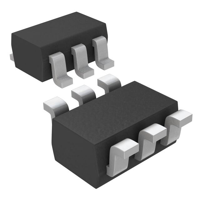
The MAX8640Y/MAX8640Z are available in the tiny 6pin, SC70 (2.0mm x 2.1mm) and µDFN (1.5mm x
1.0mm) packages. Both packages are lead-free.
Applications
Features
o
o
o
o
o
o
o
o
o
o
o
Tiny SC70 and µDFN Packages
500mA Guaranteed Output Current
4MHz or 2MHz PWM Switching Frequency
Tiny External Components: 1µH/2.2µF or
2.2µH/4.7µF
28µA Quiescent Current
Factory Preset Outputs from 0.8V to 2.5V
±1% Initial Accuracy
Low Output Ripple at All Loads
Ultrasonic Skip Mode Down to 1mA Loads
Ultra-Fast Line- and Load-Transient Response
Fast Soft-Start Eliminates Inrush Current
Ordering Information
PINPACKAGE
PART*
TOP MARK
MAX8640YEXT08+T
6 SC70
ACQ
MAX8640YEXT10+T
6 SC70
ADF
MAX8640YEXT11+T
6 SC70
ACR
MAX8640YEXT12+T
6 SC70
ACS
MAX8640YEXT13+T
6 SC70
ACG
MAX8640YEXT15+T
6 SC70
ADD
Microprocessor/DSP Core Power
MAX8640YEXT16+T
6 SC70
ADB
I/O Power
MAX8640YEXT18+T
6 SC70
ACI
Cell Phones, PDAs, DSCs, MP3s
MAX8640YEXT19+T
6 SC70
ACH
Other Handhelds Where Space Is Limited
MAX8640YEXT82+T
6 SC70
ADJ
*Contact factory for availability of each version. For 2.85V output
(82 version), request application note that includes limitations
and typical operating characteristics.
+Denotes a lead(Pb)-free/RoHS-compliant package.
T = Tape and reel.
Note: All devices are specified over the -40°C to +85°C
operating temperature range.
Ordering Information continued and Selector Guide appears
at end of data sheet.
Pin Configurations
Typical Operating Circuit
L1
1µH OR 2.2µH
INPUT
2.7V TO 5.5V
IN
GND
ON/OFF
TOP VIEW
+
+
LX
1
6
IN
LX
MAX8640Y
MAX8640Z
C1
2.2µF
OUTPUT
0.8V TO 2.5V
UP TO 500mA
SHDN
GND
2
OUT
3
MAX8640Y
MAX8640Z
LX
1
6
IN
MAX8640Y
MAX8640Z
5
GND
4
SHDN
GND
2
5
GND
OUT
3
4
SHDN
OUT
C2
2.2µF OR
4.7µF
SC70
2.0mm x 2.1mm
For pricing, delivery, and ordering information, please contact Maxim Direct
at 1-888-629-4642, or visit Maxim’s website at www.maximintegrated.com.
µDFN
1.5mm x 1.0mm
19-3997; Rev 5; 8/14
�MAX8640Y/MAX8640Z
Tiny 500mA, 4MHz/2MHz Synchronous
Step-Down DC-DC Converters
ABSOLUTE MAXIMUM RATINGS
IN to GND .................................................................-0.3V to +6V
OUT, SHDN to GND ....................................-0.3V to (VIN + 0.3V)
LX Current (Note 1) ........................................................0.8ARMS
OUTPUT Short Circuit to GND ...................................Continuous
Continuous Power Dissipation (TA = +70°C)
6-Pin SC70 (derate 3.1mW/°C above +70°C) ..............245mW
6-Pin µDFN (derate 2.1mW/°C above +70°C) ..............167.7mW
Operating Temperature Range ...........................-40°C to +85°C
Junction Temperature ......................................................+150°C
Storage Temperature Range .............................-65°C to +150°C
Lead Temperature (soldering, 10s) .................................+300°C
Note 1: LX has internal clamp diodes to IN and GND. Applications that forward bias these diodes should not exceed the IC’s package
power-dissipation limit.
Stresses beyond those listed under “Absolute Maximum Ratings” may cause permanent damage to the device. These are stress ratings only, and functional
operation of the device at these or any other conditions beyond those indicated in the operational sections of the specifications is not implied. Exposure to
absolute maximum rating conditions for extended periods may affect device reliability.
ELECTRICAL CHARACTERISTICS
(VIN = 3.6V, SHDN = IN, TA = -40°C to +85°C, typical values are at TA = +25°C, unless otherwise noted.) (Note 2)
PARAMETER
Supply Range
UVLO Threshold
SYMBOL
CONDITIONS
TYP
MAX
5.5
V
2.6
2.70
V
28
48
TA = +25°C
0.01
0.1
µA
TA = +85°C
0.1
2.5
V
VIN
UVLO
MIN
2.7
VIN rising, 100mV hysteresis
2.44
No load, no switching
Supply Current
Output Voltage Range
ICC
VOUT
Output Voltage Accuracy
(Falling Edge)
Output Load Regulation
(Voltage Positioning)
SHDN = GND
Factory preset
0.8
ILOAD = 0mA, TA = +25°C
-1
ILOAD = 0mA, TA = -40°C to +85°C
-2
Equal to inductor DC resistance
0
+1
+2
RL
UNITS
%
V/A
VIH
VIN = 2.7V to 5.5V
VIL
VIN = 2.7V to 5.5V
SHDN Input Bias Current
IIH,IL
VIN = 5.5V,
SHDN = GND or IN
Minimum Required SHDN Reset
Time
tSHDN
Peak Current Limit
ILIMP
pFET switch
590
770
1400
mA
SHDN Logic Input Level
Valley Current Limit
Rectifier Off-Current Threshold
On-Resistance
LX Leakage Current
Minimum On and Off Times
Thermal Shutdown
Thermal-Shutdown Hysteresis
1.4
0.4
TA = +25°C
0.001
TA = +85°C
0.01
1
10
V
µA
µs
ILIMN
nFET rectifier
450
650
1300
mA
ILXOFF
nFET rectifier
10
40
70
mA
RONP
pFET switch, ILX = -40mA
0.6
1.2
RONN
nFET rectifier, ILX = 40mA
0.35
0.7
ILXLKG
VIN = 5.5V, LX = GND
to IN, SHDN = GND
TA = +25°C
0.1
1
TA = +85°C
1
tON(MIN)
95
tOFF(MIN)
95
Ω
µA
ns
+160
°C
20
°C
Note 2: All devices are 100% production tested at TA = +25°C. Limits over the operating temperature range are guaranteed by design.
2
Maxim Integrated
�MAX8640Y/MAX8640Z
Tiny 500mA, 4MHz/2MHz Synchronous
Step-Down DC-DC Converters
Typical Operating Characteristics
(VIN = 3.6V, VOUT = 1.5V, MAX8640Z, L = Murata LQH32CN series, TA = +25°C, unless otherwise noted.)
70
60
50
40
30
20
MAX8640YEXT18
30
SUPPLY CURRENT (μA)
80
EFFICIENCY (%)
35
25
MAX8640ZEXT15
20
15
10
10
MAX8640ZEXT15
SWITCHING FREQUENCY (MHz)
MAX8640YEXT18
MAX8640Y/Z toc02
90
MAX8640Y/Z toc01
100
SWITCHING FREQUENCY
vs. LOAD CURRENT
NO-LOAD SUPPLY CURRENT
vs. SUPPLY VOLTAGE
MAX8640Y/Z toc03
EFFICIENCY vs. LOAD CURRENT
1.8V OUTPUT
1
MAX8640YEXT18
10
0
0.1
5
0.1
1
10
100
LOAD CURRENT (mA)
1000
2.7
3.1
3.5
3.9
4.3
4.7
5.1
0
SUPPLY VOLTAGE (V)
MAX8640ZEXT15
1.50
200
300
400
LOAD CURRENT (mA)
500
MAX8640Y/Z toc05
MAX8640Y/Z toc04
1.55
100
LIGHT-LOAD SWITCHING WAVEFORMS
(IOUT = 1mA)
OUTPUT VOLTAGE vs. LOAD CURRENT
(VOLTAGE POSITIONING)
OUTPUT VOLTAGE (V)
5.5
20mV/div
(AC-COUPLED)
VOUT
1.45
VLX
2V/div
1.40
1.35
ILX
200mA/div
1.30
0
100
200
300
400
LOAD CURRENT (mA)
10μs/div
500
MEDIUM-LOAD SWITCHING WAVEFORMS
(IOUT = 40mA)
HEAVY-LOAD SWITCHING WAVEFORMS
(IOUT = 300mA)
MAX8640Y/Z toc06
MAX8640Y/Z toc07
20mV/div
(AC-COUPLED)
VOUT
20mV/div
(AC-COUPLED)
VOUT
2V/div
VLX
2V/div
0V
VLX
0V
200mA/div
200mA/div
ILX
0mA
200ns/div
Maxim Integrated
ILX
0mA
200ns/div
3
�MAX8640Y/MAX8640Z
Tiny 500mA, 4MHz/2MHz Synchronous
Step-Down DC-DC Converters
Typical Operating Characteristics (continued)
(VIN = 3.6V, VOUT = 1.5V, MAX8640Z, L = Murata LQH32CN series, TA = +25°C, unless otherwise noted.)
LIGHT-LOAD STARTUP WAVEFORM
(100Ω LOAD)
HEAVY-LOAD STARTUP WAVEFORM
(5Ω LOAD)
MAX8640Y/Z toc08
MAX8640Y/Z toc09
5V/div
VSHDN
5V/div
VSHDN
1V/div
1V/div
VOUT
0V
VOUT
0V
100mA/div
100mA/div
0mA
IIN
IIN
0mA
ILX
500mA/div
500mA/div
ILX
0mA
0mA
20μs/div
20μs/div
LINE-TRANSIENT RESPONSE
(4V TO 3.5V TO 4V)
LOAD-TRANSIENT RESPONSE
(5mA TO 250mA TO 5mA)
MAX8640Y/Z toc10
MAX8640Y/Z toc11
1V/div
4V
VIN
VOUT
50m/div
AC-COUPLED
VOUT
500mA/div
ILX
20mV/div
AC-COUPLED
200mA/div
IOUT
200mA/div
ILX
0mA
0mA
20μs/div
40μs/div
LOAD-TRANSIENT RESPONSE
(10mA TO 500mA TO 10mA)
MAX8640Y/Z toc12
100mV/div
AC-COUPLED
VOUT
500mA/div
ILX
0V
IOUT
200mA/div
40μs/div
4
Maxim Integrated
�MAX8640Y/MAX8640Z
Tiny 500mA, 4MHz/2MHz Synchronous
Step-Down DC-DC Converters
Pin Description
PIN
NAME
FUNCTION
1
LX
2, 5
GND
Ground. Connect these pins together directly under the IC.
3
OUT
Output Sense Input. Bypass with a ceramic capacitor as close as possible to pin 3 (OUT) and pin 2 (GND).
OUT is internally connected to the internal feedback network.
4
SHDN
6
IN
Inductor Connection to the Internal Drains of the p-channel and n-channel MOSFETs. High impedance
during shutdown.
Active-Low Shutdown Input. A logic-low on SHDN disables the step-down DC-DC and resets the logic. A logichigh on SHDN enables the step-down DC-DC. Ensure that SHDN is low for ≥ 10µs (tSHDN) after VIN rises above its
undervoltage lockout threshold (UVLO) to reset the logic. See the Shutdown Mode section for more information.
Supply Voltage Input. Input voltage range is 2.7V to 5.5V. Bypass with a ceramic capacitor as close as
possible to pin 6 (IN) and pin 5 (GND).
Detailed Description
The MAX8640Y/MAX8640Z step-down converters deliver over 500mA to outputs from 0.8V to 2.5V. They utilize
a proprietary hysteretic PWM control scheme that
switches at up to 4MHz (MAX8640Z) or 2MHz
(MAX8640Y), allowing some trade-off between efficiency and size of external components. At loads below
100mA, the MAX8640Y/MAX8640Z automatically switch
to pulse-skipping mode to minimize the typical quiescent current (28µA). Output ripple remains low at all
loads, while the skip-mode switching frequency
remains ultrasonic down to 1mA (typ) loads. Figure 1 is
the simplified functional diagram.
Control Scheme
A proprietary hysteretic PWM control scheme ensures
high efficiency, fast switching, fast transient response,
low output ripple, and physically tiny external components. This control scheme is simple: when the output
voltage is below the regulation threshold, the error
comparator begins a switching cycle by turning on the
high-side switch. This switch remains on until the minimum on-time expires and the output voltage is above
the regulation threshold or the inductor current is above
the current-limit threshold. Once off, the high-side
switch remains off until the minimum off-time expires
and the output voltage falls again below the regulation
threshold. During the off period, the low-side synchronous rectifier turns on and remains on until either the
high-side switch turns on again or the inductor current
approaches zero. The internal synchronous rectifier
eliminates the need for an external Schottky diode.
Maxim Integrated
Voltage-Positioning Load Regulation
The MAX8640Y/MAX8640Z utilize a unique feedback
network. By taking DC feedback from the LX node, the
usual phase lag due to the output capacitor is
removed, making the loop exceedingly stable and
allowing the use of very small ceramic output capacitors.
This configuration yields load regulation equal to the
inductor’s series resistance multiplied by the load current.
This voltage-positioning load regulation greatly reduces
overshoot during load transients, effectively halving the
peak-to-peak output-voltage excursions compared to traditional step-down converters. See the Load-Transient
Response in the Typical Operating Characteristics.
Shutdown Mode
A logic-low on SHDN places the MAX8640Y/MAX8640Z
in shutdown mode by disabling the step-down DC-DC
and resetting its logic. In shutdown mode, the supply
current (ICC) is reduced to 0.01µA typical. Additionally,
the power MOSFETs between IN, LX, and GND
(Figure 1) are open such that LX is high impedance.
Ensure that SHDN is low for ≥ 10µs (tSHDN) after VIN
rises above its undervoltage lockout threshold (UVLO)
to reset the logic. In the majority of systems, this tSHDN
requirement is fulfilled naturally because the upstream
logic controlling SHDN is powered off of the same VIN
as the MAX8640Y/MAX8640Z. However, systems that
want an always on regulator without the burden of
enable/disable logic can use an R and C circuit on
SHDN as shown in Figure 2.
5
�MAX8640Y/MAX8640Z
Tiny 500mA, 4MHz/2MHz Synchronous
Step-Down DC-DC Converters
as Li+ and alkaline cells. See the Soft-Start Response
in the Typical Operating Characteristics.
IN
SHDN
PWM
LOGIC
LX
Applications Information
The MAX8640Y/MAX8640Z are optimized for use with a
tiny inductor and small ceramic capacitors. The correct
selection of external components ensures high efficiency, low output ripple, and fast transient response.
Inductor Selection
GND
OUT
0.6V
MAX8640Y
MAX8640Z
Figure 1. Simplified Functional Diagram
MAX8640
IN
ESD
DIODE
100kΩ
VIN
SHDN
4.7nF
GND
Figure 2. Using an R and C circuit to create an always on regulator
Soft-Start
The MAX8640Y/MAX8640Z include internal soft-start
circuitry that eliminates inrush current at startup, reducing transients on the input source. Soft-start is particularly useful for higher impedance input sources, such
6
A 1µH inductor is recommended for use with the
MAX8640Z, and 2.2µH is recommended for the
MAX8640Y. A 1µH inductor is physically smaller but
requires faster switching, resulting in some efficiency
loss. Table 1 lists several recommended inductors.
It is acceptable to use a 1.5µH inductor with either the
MAX8640Y or MAX8640Z, but efficiency and ripple
should be verified. Similarly, it is acceptable to use a
3.3µH inductor with the MAX8640Y, but performance
should be verified.
For optimum voltage positioning of load transients,
choose an inductor with DC series resistance in the
75mΩ to 150mΩ range. For higher efficiency at heavy
loads (above 200mA) or minimal load regulation (but
some transient overshoot), the resistance should be
kept as low as possible. For light-load applications up
to 200mA, higher resistance is acceptable with very little impact on performance.
Capacitor Selection
Output Capacitor
The output capacitor, C2, is required to keep the output
voltage ripple small and to ensure regulation loop stability. C2 must have low impedance at the switching frequency. Ceramic capacitors are recommended due to
their small size and low ESR. Make sure the capacitor
maintains its capacitance over temperature and DC
bias. Capacitors with X5R or X7R temperature characteristics typically perform well. The output capacitance
can be very low; see the Selector Guide for recommended capacitance values. For optimum load-transient performance and very low output ripple, the output
capacitor value in µF should be equal to or larger than
the inductor value in µH.
Maxim Integrated
�MAX8640Y/MAX8640Z
Tiny 500mA, 4MHz/2MHz Synchronous
Step-Down DC-DC Converters
Table 1. Suggested Inductors
MANUFACTURER
SERIES
MIPFT2520D
FDK
Murata
Sumida
Taiyo Yuden
MIPF2520D
LQM31P
CDRH2D09
CKP3216T
GLF201208T
TDK
GLF2012T
GLF251812T
MDT2520-CR
TOKO
D2812C
INDUCTANCE
(µH)
DC RESISTANCE
(Ω typ)
DIMENSIONS
L x W x H (mm)
2.5 x 2.0 x 0.5
2.0
0.16
900
1.5
0.07
1500
2.2
0.08
1300
3.3
0.10
1200
1.0
0.12
1200
1.5
0.16
1000
2.2
0.22
900
1.2
0.08
590
1.5
0.09
520
2.2
0.12
440
1.0
0.11
1100
1.5
0.13
1000
2.2
0.14
900
1.0
0.15
460
2.2
0.36
300
1.0
0.07
400
2.2
0.10
300
1.0
0.10
800
2.2
0.20
600
1.0
0.05
1000
2.2
0.08
700
1.0
0.07
1100
2.2
0.14
770
Input Capacitor
The input capacitor, C1, reduces the current peaks
drawn from the battery or input power source and
reduces switching noise in the IC. The impedance of C1
at the switching frequency should be kept very low.
Ceramic capacitors are recommended due to their
small size and low ESR. Make sure the capacitor maintains its capacitance over temperature and DC bias.
Capacitors with X5R or X7R temperature characteristics
typically perform well. Due to the MAX8640Y/
MAX8640Z soft-start, the input capacitance can be very
low. For optimum noise immunity and low input ripple,
choose a capacitor value in µF that is equal to or larger
than the inductor’s value in µH.
Maxim Integrated
CURRENT RATING
(mA)
2.5 x 2.0 x 1.0
3.2 x 1.6 x 0.95
3.0 x 3.0 x 1.0
3.2 x 1.6 x 0.9
2.0 x 1.25 x 0.9
2.0 x 1.25 x 1.35
2.5 x 1.8 x 1.35
2.5 x 2.0 x 1.0
2.8 x 2.8 x 1.2
PCB Layout and Routing
High switching frequencies and large peak currents
make PCB layout a very important part of design. Good
design minimizes excessive EMI on the feedback paths
and voltage gradients in the ground plane, both of
which can result in instability or regulation errors.
Connect the inductor, input capacitor, and output
capacitor as close together as possible, and keep their
traces short, direct, and wide. Connect the two GND
pins under the IC and directly to the grounds of the
input and output capacitors. Keep noisy traces, such
as the LX node, as short as possible. Refer to the
MAX8640Z evaluation kit for an example PCB layout
and routing scheme.
7
�MAX8640Y/MAX8640Z
Tiny 500mA, 4MHz/2MHz Synchronous
Step-Down DC-DC Converters
Selector Guide
8
PART
OUTPUT
VOLTAGE (V)
FREQUENCY
(MHz)
MAX8640YEXT08
0.8
MAX8640YEXT10
RECOMMENDED COMPONENTS
TOP MARK
L1 (µH)
C2 (µF)
1.2
2.2
10
1.0
1.6
2.2
4.7
ADF
MAX8640YEXT11
1.1
1.7
2.2
4.7
ACR
MAX8640YEXT12
1.2
1.8
2.2
4.7
ACS
ACG
ACQ
MAX8640YEXT13
1.3
1.9
2.2
4.7
MAX8640YEXT15
1.5
2.0
2.2
4.7
ADD
MAX8640YEXT16
1.6
2.0
2.2
4.7
ADB
ACI
MAX8640YEXT18
1.8
2.0
2.2
4.7
MAX8640YEXT19
1.9
2.0
2.2
4.7
ACH
MAX8640YEXT24
2.4
2.0
2.2
4.7
ADM
ACJ
MAX8640YEXT25
2.5
1.7
2.2
4.7
MAX8640YEXT82
MAX8640YELT08
2.85
0.8
1.5
1.2
2.2
2.2
4.7
10
ADJ
NB
MAX8640YELT11
1.1
1.7
2.2
4.7
NC
MAX8640YELT12
1.2
1.8
2.2
4.7
ND
MAX8640YELT13
1.3
1.9
2.2
4.7
NE
MAX8640YELT15
1.5
2.0
2.2
4.7
NF
MAX8640YELT16
1.6
2.0
2.2
4.7
NG
MAX8640YELT18
1.8
2.0
2.2
4.7
NH
MAX8640YELT19
1.9
2.0
2.2
4.7
NI
MAX8640YELT25
2.5
1.7
2.2
4.7
NJ
MAX8640YELT82
2.85
1.5
2.2
4.7
OW
MAX8640ZEXT08
0.8
2.4
1
4.7
ACL
MAX8640ZEXT11
1.1
3.4
1
2.2
ACM
MAX8640ZEXT12
1.2
3.6
1
2.2
ACN
MAX8640ZEXT13
1.3
3.7
1
2.2
ACO
MAX8640ZEXT15
1.5
3.9
1
2.2
ACP
ACU
MAX8640ZEXT18
1.8
4.0
1
2.2
MAX8640ZELT08
0.8
2.4
1
4.7
NK
MAX8640ZELT11
1.1
3.4
1
2.2
NL
Maxim Integrated
�MAX8640Y/MAX8640Z
Tiny 500mA, 4MHz/2MHz Synchronous
Step-Down DC-DC Converters
Selector Guide (continued)
PART
OUTPUT
VOLTAGE (V)
FREQUENCY
(MHz)
MAX8640ZELT12
1.2
3.6
RECOMMENDED COMPONENTS
TOP MARK
L1 (µH)
C2 (µF)
1
2.2
NN
NM
MAX8640ZELT13
1.3
3.7
1
2.2
MAX8640ZELT15
1.5
3.9
1
2.2
NO
MAX8640ZELT18
1.8
4.0
1
2.2
NP
Ordering Information (continued)
PART*
PINPACKAGE
TOP MARK
PART*
PINPACKAGE
TOP MARK
MAX8640YEXT24+T
6 SC70
ADM
MAX8640ZEXT08+T
6 SC70
ACL
MAX8640YEXT25+T
MAX8640YELT08+T
6 SC70
6 µDFN
ACJ
NB
MAX8640ZEXT11+T
6 SC70
ACM
MAX8640ZEXT12+T
6 SC70
ACN
MAX8640YELT11+T
6 µDFN
NC
MAX8640ZEXT13+T
6 SC70
ACO
MAX8640YELT12+T
6 µDFN
ND
MAX8640ZEXT15+T
6 SC70
ACP
MAX8640YELT13+T
6 µDFN
NE
MAX8640ZEXT18+T
6 SC70
ACU
MAX8640YELT15+T
6 µDFN
NF
MAX8640ZELT08+T
6 µDFN
NK
MAX8640YELT16+T
6 µDFN
NG
MAX8640ZELT11+T
6 µDFN
NL
MAX8640YELT18+T
6 µDFN
NH
MAX8640ZELT12+T
6 µDFN
NM
MAX8640YELT19+T
6 µDFN
NI
MAX8640ZELT13+T
6 µDFN
NN
MAX8640YELT25+T
6 µDFN
NJ
MAX8640ZELT15+T
6 µDFN
NO
MAX8640YELT82+T
6 µDFN
OW
MAX8640ZELT18+T
6 µDFN
NP
*Contact factory for availability of each version. For 2.85V output
(82 version), request application note that includes limitations
and typical operating characteristics.
+Denotes a lead(Pb)-free/RoHS-compliant package.
T = Tape and reel.
Note: All devices are specified over the -40°C to +85°C
operating temperature range.
Maxim Integrated
Chip Information
PROCESS: BiCMOS
9
�MAX8640Y/MAX8640Z
Tiny 500mA, 4MHz/2MHz Synchronous
Step-Down DC-DC Converters
Package Information
For the latest package outline information and land patterns (footprints), go to www.maximintegrated.com/packages. Note that a “+”, “#”, or
“-” in the package code indicates RoHS status only. Package drawings may show a different suffix character, but the drawing pertains to the
package regardless of RoHS status.
PACKAGE TYPE
PACKAGE CODE
DOCUMENT NO.
6 µDFN
L611-1
21-0147
6 SC70
X6S-1
21-0077
SCOTT SCHROEDER
01/12/12
10
Maxim Integrated
�MAX8640Y/MAX8640Z
Tiny 500mA, 4MHz/2MHz Synchronous
Step-Down DC-DC Converters
Package Information (continued)
For the latest package outline information and land patterns (footprints), go to www.maximintegrated.com/packages. Note that a “+”, “#”, or
“-” in the package code indicates RoHS status only. Package drawings may show a different suffix character, but the drawing pertains to the
package regardless of RoHS status.
SCOTT SCHROEDER
01/12/12
Maxim Integrated
11
�MAX8640Y/MAX8640Z
Tiny 500mA, 4MHz/2MHz Synchronous
Step-Down DC-DC Converters
Package Information (continued)
For the latest package outline information and land patterns (footprints), go to www.maximintegrated.com/packages. Note that a “+”, “#”, or
“-” in the package code indicates RoHS status only. Package drawings may show a different suffix character, but the drawing pertains to the
package regardless of RoHS status.
12
Maxim Integrated
�MAX8640Y/MAX8640Z
Tiny 500mA, 4MHz/2MHz Synchronous
Step-Down DC-DC Converters
Revision History
REVISION
NUMBER
REVISION
DATE
3
6/08
Added MAX8640YEXT10+T voltage option
4
2/09
Added MAX8640YEXT24+T voltage option and
MAX8640YELT82+MAX8640YEXT82+ (82 = 2.85V), and corrected error
5
8/14
Updated Electrical Characteristics table, Pin Description, and Shutdown Mode
sections
DESCRIPTION
PAGES
CHANGED
7
1, 2, 7, 8
2, 5
Maxim Integrated cannot assume responsibility for use of any circuitry other than circuitry entirely embodied in a Maxim Integrated product. No circuit patent
licenses are implied. Maxim Integrated reserves the right to change the circuitry and specifications without notice at any time. The parametric values (min and
max limits) shown in the Electrical Characteristics table are guaranteed. Other parametric values quoted in this data sheet are provided for guidance.
Maxim Integrated 160 Rio Robles, San Jose, CA 95134 USA 1-408-601-1000 ________________________________ 13
© 2014 Maxim Integrated Products, Inc.
Maxim Integrated and the Maxim Integrated logo are trademarks of Maxim Integrated Products, Inc.
�


 工商网监
湘ICP备2023018690号
工商网监
湘ICP备2023018690号
