SCOPE: CMOS, µP-Compatible, 12-Bit D/A Converter
Device Type:
-01
-02
-03
Generic Number:
MX7542S(x)/883B
MX7542T(x)/883B
MX7542GT(x)/883B
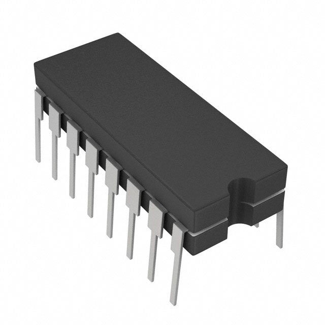
Case Outline(s).
Outline Letter
Q
E
Mil-Std-1835
GDIP1-T16 or CDIP2-T16
CQCC1-N20
Case Outline
Package Code
16 Lead CERDIP
J16
20-Pin Ceramic LCC L20
Absolute Maxi mum Ratings: (TA=+25°C, unless otherwise noted.)
VDD to AGND ........................................................................................……….... 0V, +7V
VDD to DGND ......................................................................................…..….…... 0V, +7V
AGND to DGND …………………………………………………………………….... VDD
DGND to AGND …………………………………………………………………….... VDD
Digital Input Voltage to DGND .....................................................……………. -0.3V, VDD
VOUT1, VOUT2 to AGND ...............................................……………………….... -0.3V, VDD
VREF to AGND ......................................................................................…... -25V to +25V
VRFB to AGND ......................................................................................…..... -25V to +25V
Lead Temperature (soldering, 10 seconds) ................................................................. +300°C
Storage Temperature .................................................................................... -65°C to +150°C
Continuous Power Dissipation ........................................................................….. TA=+70°C
16 pin CERDIP(derate 10mW/°C above +70°C) .................................….............….. 800mW
20 pin LCC(derate 9.09mW/°C above +70°C) .....................................................…... 727mW
Junction Temperature TJ .....................................................................................….. +150°C
Thermal Resistance, Junction to Case, ΘJC
16 pin CERDIP................................................................................................…... 50°C/W
20 pin LCC .....................................................................................................…... 20°C/W
Thermal Resistance, Junction to Ambient, ΘJA:
16 pin CERDIP..............................................................................................…... 100°C/W
20 pin LCC ...................................................................................................…... 110°C/W
Recommended Operating Conditions
Ambient Operating Range (TA) ...........................................................….. -55°C to +125°C
Stresses beyond those listed under “Absolute Maximum Ratings” may cause permanent damage to
the device.These are stress ratings only, and functional operation of the device at these or any other
conditions beyond those indicated in the operational sections of the specifications is not implied.
Exposure to absolute maximum rating conditions for extended periods may affect device reliability.
-------------------------------------
Electrical Characteristics of
MX7542/883B
19-2439
Page 2
of
Rev. B
6
�TABLE 1. ELECTRICAL TESTS:
TEST
Symbol
Resolution
Relative Accuracy
RES
RA
Differential
Nonlinearity
Gain Error
NOTE 3
Gain Error
NOTE 3
Gain Tempco
Power-Supply
Rejection
OUT1 Leakage
Current
OUT2 Leakage
Current
Output Current
Settling Time
NOTE 2
Feedthrough Error
NOTE 2
Reference Input
Resistance
Digital Input High
Voltage
Digital Input Low
Voltage
Digital Input
Leakage Current
Digital Input
Capacitance
NOTE 2
Output Capacitance
NOTE 2
DNL
CONDITIONS
1/
-55°C≤TA≤+125°C
Unless otherwise specified
NOTE 2
GROUP A
Subgroup
1,2,3
All
01
02,03
01
02,03
01,02
Limits
Min
Limits
Max
12
-1
-0.5
-2
-1
-12.3
-14.5
-1
-2
-5
-0.005
-0.01
-1
-200
-1
-200
Units
Bits
LSB
All
1
0.5
2
1
12.3
14.5
1
2
5
0.005
0.01
1
200
1
200
2
4
All
2.5
mVp-p
RIN
1,2,3
All
8
25
kΩ
VIH
1,2,3
All
3.0
VIL
1,2,3
All
1,2,3
All
4
All
Monotonic to 11 bits
Monotonic to 12 bits
AE
1
2,3
1
2,3
AE
TCAE
PSRR
IOUT1
IOUT2
tSL
FT
IIN
NOTE 2
VDD=4.75V to 5.25V
(∆Gain/∆VDD)
DAC register loaded with all
0s
DAC register loaded with all
1s
To ±0.5LSB, OUT1 load is 100
Ω || 13pF, output measured ___
from trailing edge of WR
VREF=10V, 10kHz sine wave
VIN=0V or VDD
CIN
COUT1
1,2,3
1
2,3
1
2,3
1
2,3
4
COUT2
03
All
All
All
All
-1
LSB
ppm/°C
%/%VDD
nA
nA
µs
V
1
µA
8
pF
All
pF
75
75
4
All
pF
260
Digital inputs at VIL, DAC
register loaded with all 0s
Electrical Characteristics of
MX7542/883B
LSB
260
Digital inputs at VIL, DAC
register loaded with all 0s
Digital inputs at VIH, DAC
register loaded with all 1s
-------------------------------------
LSB
V
0.8
Digital inputs at VIH, DAC
register loaded with all 1s
4
Output Capacitance
NOTE 2
Device
type
19-2439
Page 3
of
Rev. B
6
�TABLE 1. ELECTRICAL TESTS:
TEST
Symbol
Write Pulse Width
Address to WriteHold Time
Chip Select to
Write-Hold Time
Minimum Clear
Pulse Width
Chip Select to
Write-Setup Time
Address Valid to
Write-Setup Time
Data-Setup Time
Data-Hold Time
Chip Select to
Write-Setup Time
Address Valid to
Write-Setup Time
Supply Current
tWR
tAWH
CONDITIONS
1/
-55°C≤TA≤+125°C
Unless otherwise specified
NOTE 4
NOTE 4
tCWH
NOTE 1:
NOTE 2:
NOTE 3:
NOTE 4:
GROUP A
Subgroup
Device
type
Units
All
All
220
80
ns
ns
NOTE 4
9
All
100
ns
tCLR
NOTE 4
9
All
300
ns
tCWS
Byte loading, NOTE 4
9
All
130
ns
tAWS
Byte loading, NOTE 4
9
All
180
ns
tDS
tDH
tCWS
NOTE 4
NOTE 4
DAC loading, NOTE 4
9
9
9
All
All
All
350
65
150
ns
ns
ns
tAWS
DAC loading, NOTE 4
9
All
240
ns
IDD
Digital inputs = VIH or VIL
1,2,3
All
2.5
VDD=+5V, VOUT1=VOUT2=0V, VREF=+10V, unless otherwise noted.
Characteristics supplied for use as a typical design limit but not production tested.
Measured using internal feedback resistor; includes effects of leakage current and gain TC.
Timing shown in commercial datasheet.
J16
A1
DGND
AGND
OUT2
13
4
5
6
7
D3
D2
D1
D0
AGND
D3
NC
D2
14
15
16
17
8
___
CS
___
WR
A0
D1
18
A1
DGND
NC
____
CLR
VDD
D0
19
VREF
___
CS
20
RFB
-------------------------------------
____
CLR
VDD
VREF
RFB
L20
NC
___
WR
A0
3
10
Limits
Max
9
9
TERMINAL CONNECTIONS:
MX7542
J16
L20
1
OUT1
NC
11
2
OUT2
OUT1
12
9
Limits
Min
Electrical Characteristics of
MX7542/883B
19-2439
Page 4
of
Rev. B
6
mA
�ORDERING INFORMATION:
01
J16
MX7542SQ/883B
01
L20
MX7542SE/883B
02
J16
MX7542TQ/883B
02
L20
MX7542TE/883B
03
J16
MX7542GTQ/883B
03
L20
MX7542GTE/883B
QUALITY ASSURANCE
Sampling and inspection procedures shall be in accordance with Mil-Prf-38535, Appendix A as
Specified in Mil-Std-883.
Screening shall be in accordance with Method 5004 of Mil-Std-883. Burn-in test Method 1015:
1. Test Condition, A, B, C, or D.
2. TA = +125°C, minimum.
3. Interim and final electrical test requirements shall be specified in Table 2.
Quality conformance inspection shall be in accordance with Method 5005 of Mil-Std-883,
Including Groups A, B, C, and D inspection.
Group A inspection:
1. Tests as specified in Table 2.
2. Selected subgroups in Table 1, Method 5005 of Mil-Std-883 shall be omitted.
Group C and D inspections:
a. End-point electrical parameters shall be specified in Table 1.
b. Steady-state life test, Method 1005 of Mil-Std-883.
1. Test condition A, B, C, D.
2. TA = +125°C, minimum.
3. Test duration, 1000 hours, except as permitted by Method 1005 of Mil-Std-883.
TABLE 2.
ELECTRICAL TEST REQUIREMENTS
Mil-Std-883 Test Requirements
Interim Electric Parameters
Method 5004
Final Electrical Parameters
Method 5005
Group A Test Requirements
Method 5005
Group C and D End-Point Electrical Parameters
Method 5005
Subgroups
Per Method 5005, Table 1
1
1*, 2, 3
1, 2, 3, 4** 9
1
* PDA applies to Subgroup 1 only.
** Subgroup 4 shall be tested at initial qualification and upon redesign. Sample size will be 116 units.
-------------------------------------
Electrical Characteristics of
MX7542/883B
19-2439
Page 5
of
Rev. B
6
��


 工商网监
湘ICP备2023018690号
工商网监
湘ICP备2023018690号
