eGaN® FET DATASHEET
EPC2106
EPC2106 – Enhancement-Mode GaN Power
Transistor Half-Bridge
VDS , 100 V
RDS(on) , 70 mΩ
ID , 1.7 A
EFFICIENT POWER CONVERSION
HAL
Gallium Nitride’s exceptionally high electron mobility and low temperature coefficient allows very
low RDS(on), while its lateral device structure and majority carrier diode provide exceptionally low QG
and zero QRR. The end result is a device that can handle tasks where very high switching frequency,
and low on-time are beneficial as well as those where on-state losses dominate.
Maximum Ratings
DEVICE
PARAMETER
VDS
ID
Q1
&
Q2
VALUE
Drain-to-Source Voltage (Continuous)
100
Drain-to-Source Voltage (up to 10,000 5 ms pulses at 150°C)
120
Continuous (TA = 25°C, RθJA = 320°C/W)
1.7
Pulsed (25°C, TPULSE = 300 µs)
18
Gate-to-Source Voltage
6
Gate-to-Source Voltage
–4
TJ
Operating Temperature
–40 to 150
TSTG
Storage Temperature
–40 to 150
VGS
UNIT
V
A
V
°C
Thermal Characteristics
PARAMETER
TYP
RθJC
Thermal Resistance, Junction-to-Case
3
RθJB
Thermal Resistance, Junction-to-Board
30
RθJA
Thermal Resistance, Junction-to-Ambient (Note 1)
81
UNIT
EPC2106 eGaN® ICs are supplied only in
passivated die form with solder bumps
Die size: 1.35 mm x 1.35 mm
Applications
• High Frequency DC-DC Conversion
• Class-D Audio
Benefits
• Ultra High Efficiency
• Ultra Low RDS(on)
• Ultra Low QG
• Ultra Small Footprint
°C/W
Note 1: RθJA is determined with the device mounted on one square inch of copper pad, single layer 2 oz copper on FR4 board.
See https://epc-co.com/epc/documents/product-training/Appnote_Thermal_Performance_of_eGaN_FETs.pdf for details
4
7
Q1
Q1
Level Shift
5V
1
Output
C Bus
3
Gate
Driver
Typical Application Circuit
EPC – POWER CONVERSION TECHNOLOGY LEADER | EPC-CO.COM | ©2021 |
G1
S1
D2
Q2
Q2
D1
2
5
8
G2
S2
6
9
EPC2106 – Detailed Schematic
| 1
�eGaN® FET DATASHEET
DEVICE
PARAMETER
BVDSS
Drain-to-Source Voltage
VGS = 0 V, ID = 0.3 mA
Drain-Source Leakage
VDS = 80 V, VGS = 0 V
MIN
TYP
MAX
UNIT
0.001
0.25
mA
100
V
Gate-to-Source Forward Leakage
VGS = 5 V
0.01
1
mA
Gate-to-Source Reverse Leakage
VGS = -4 V
0.001
0.25
mA
VGS(TH)
Gate Threshold Voltage
RDS(on)
Drain-Source On Resistance
VSD
Source-Drain Forward Voltage
VDS = VGS, ID = 0.6 mA
1.4
2.5
V
VGS = 5 V, ID = 2 A
0.8
55
70
mΩ
IS = 0.35 A, VGS = 0 V
2.1
Dynamic Characteristics (TJ= 25˚C unless otherwise stated)
PARAMETER
TEST CONDITIONS
DEVICE
Q2
Static Characteristics (TJ= 25˚C unless otherwise stated)
TEST CONDITIONS
IDSS
IGSS
Q1 & Q2
Q1
EPC2106
CISS
Input Capacitance
CRSS
Reverse Transfer Capacitance
COSS
Output Capacitance
COSS(ER)
Effective Output Capacitance, Enegy Related (Note 2)
COSS(TR)
Effective Output Capacitance, Time Related (Note 3)
RG
Gate Resistance
QG
Total Gate Charge
VDS = 50 V, VGS = 0 V
MIN
V
TYP
MAX
79
95
0.5
52
VDS = 0 to 50 V, VGS = 0 V
63
730
QGS
Gate to Source Charge
Gate to Drain Charge
QG(TH)
Gate Charge at Threshold
QOSS
Output Charge
QRR
Source-Drain Recovery Charge
0
CISS
Input Capacitance
79
CRSS
Reverse Transfer Capacitance
COSS
Output Capacitance
COSS(ER)
Effective Output Capacitance, Enegy Related (Note 2)
COSS(TR)
Effective Output Capacitance, Time Related (Note 3)
Gate Resistance
QG
Total Gate Charge
QGS
Gate to Source Charge
QGD
Gate to Drain Charge
QG(TH)
Gate Charge at Threshold
QOSS
Output Charge
QRR
Source-Drain Recovery Charge
pF
79
QGD
RG
78
1.3
VDS = 50 V, VGS = 5 V, ID = 2 A
UNIT
Ω
900
240
VDS = 50 V, ID = 2 A
140
pC
165
VDS = 50 V, VGS = 0 V
VDS = 50 V, VGS = 0 V
3960
95
0.5
61
VDS = 0 to 50 V, VGS = 0 V
5940
92
74
94
1.8
VDS = 50 V, VGS = 5 V, ID = 2 A
pF
730
Ω
900
240
VDS = 50 V, ID = 2 A
140
pC
165
VDS = 50 V, VGS = 0 V
4680
7020
0
Note 2: COSS(ER) is a fixed capacitance that gives the same stored energy as COSS while VDS is rising from 0 to 50% BVDSS.
Note 3: COSS(ER) is a fixed capacitance that gives the same charging time as COSS while VDS is rising from 0 to 50% BVDSS.
EPC – POWER CONVERSION TECHNOLOGY LEADER | EPC-CO.COM | ©2021 |
| 2
�eGaN® FET DATASHEET
EPC2106
Figure 1 (Q1 & Q2): Typical Output Characteristics at 25°C
15
VGS = 5 V
VGS = 4 V
ID – Drain Current (A)
ID – Drain Current (A)
15
Figure 2 (Q1 & Q2): Transfer Characteristics
VGS = 3 V
VGS = 2 V
10
5
0
0
0.5
1.0
1.5
2.0
2.5
VDS – Drain-to-Source Voltage (V)
VDS = 3 V
10
5
0
3.0
25˚C
125˚C
0.5
RDS(on) – Drain-to-Source Resistance (mΩ)
RDS(on) – Drain-to-Source Resistance (mΩ)
200
ID = 1 A
ID = 2A
ID = 3 A
ID = 4 A
100
50
0
2.5
3.0
3.5
4.0
4.5
1.5
2.5
3.0
3.5
4.0
4.5
5.0
200
25˚C
125˚C
150
100
50
0
5.0
ID = 2 A
2.5
3.0
3.5
4.0
4.5
VGS – Gate-to-Source Voltage (V)
VGS – Gate-to-Source Voltage (V)
5.0
Figure 5b (Q1): Capacitance (Log Scale)
Figure 5a (Q1): Capacitance (Linear Scale)
1000
150
COSS = CGD + CSD
CISS = CGD + CGS
CRSS = CGD
100
100
Capacitance (pF)
Capacitance (pF)
2.0
VGS – Gate-to-Source Voltage (V)
Figure 4 (Q1 & Q2): RDS(on) vs. VGS for Various Temperatures
Figure 3 (Q1 & Q2): RDS(on) vs. VGS for Various Drain Currents
150
1.0
10
COSS = CGD + CSD
CISS = CGD + CGS
CRSS = CGD
50
1
0
0
25
50
75
100
VDS – Drain-to-Source Voltage (V)
EPC – POWER CONVERSION TECHNOLOGY LEADER | EPC-CO.COM | ©2021 |
0.1
0
25
50
75
100
VDS – Drain-to-Source Voltage (V)
| 3
�eGaN® FET DATASHEET
EPC2106
Figure 5c (Q2): Capacitance (Linear Scale)
Figure 5d (Q2): Capacitance (Log Scale)
1000
200
COSS = CGD + CSD
CISS = CGD + CGS
CRSS = CGD
100
Capacitance (pF)
100
1
50
0
COSS = CGD + CSD
CISS = CGD + CGS
CRSS = CGD
10
0
25
50
75
0.1
100
0
25
VDS – Drain-to-Source Voltage (V)
75
100
Figure 6a
6a:(Q1):
Output
Output
Charge
Charge
and Cand
COSS Stored
Energy
Energy
OSS Stored
Figure 6b
6a:(Q2):
Output
Output
Charge
Charge
and Cand
COSS Stored
Energy
Energy
OSS Stored
320
6
240
7
280
5
200
6
240
200
160
5
4
4
160
3
120
2
80
40
QOSS – Output Charge (nC)
8
EOSS – COSS Stored Energy (μJ)
280
7
QOSS – Output Charge (nC)
50
VDS – Drain-to-Source Voltage (V)
3
120
2
80
1
40
1
0
0
0
0
25
50
75
100
0
25
50
EOSS – COSS Stored Energy (μJ)
Capacitance (pF)
150
0
100
75
VDS – Drain-to-Source Voltage (V)
VDS – Drain-to-Source Voltage (V)
Figure 8 (Q1 & Q2): Reverse Drain-Source Characteristics
Figure 7 (Q1 & Q2): Gate Charge
ID = 2 A
VDS = 50 V
4
ISD – Source-to-Drain Current (A)
VGS – Gate-to-Source Voltage (V)
5
3
2
1
0
0
200
400
QG – Gate Charge (pC)
600
800
EPC – POWER CONVERSION TECHNOLOGY LEADER | EPC-CO.COM | ©2021 |
25˚C
125˚C
15
VGSDS = 03 V
10
5
0
0
0.5
1.0
1.5
2.0
2.5
3.0
3.5
VSD – Source-to-Drain Voltage (V)
4.0
4.5
5.0
| 4
�eGaN® FET DATASHEET
Figure 10 (Q1 & Q2):
Normalized Threshold Voltage vs. Temperature
Figure 9 (Q1 & Q2):
Normalized On-State Resistance vs. Temperature
1.40
1.30
1.8
Normalized Threshold Voltage
Normalized On-State Resistance RDS(on)
2.0
EPC2106
ID = 2 A
VGS = 5 V
1.6
1.4
1.2
1.0
0.8
1.20
ID = 0.6 mA
1.10
1.00
0.90
0.80
0.70
0
25
50
75
100
TJ – Junction Temperature (°C)
125
0.60
150
0
25
50
75
100
TJ – Junction Temperature (°C)
125
150
ZθJB, Normalized Thermal Impedance
(Q1 & Q2) Junction-to-Board
1 Duty Cycle:
0.5
0.1
0.1
0.05
0.02
0.01
0.01
PDM
t1
0.001
Single Pulse
0.0001
10-5
10-4
t2
Notes:
Single
Duty Factor:
D Pulse
= t1/t2
Peak TJ = PDM x ZθJB x RθJB + TB
10-3
10-2
10-1
1
101
tp, Rectangular Pulse Duration, seconds
(Q1 & Q2) Junction-to-Case
ZθJC, Normalized Thermal Impedance
1
0.10
Duty Cycle:
0.5
0.2
0.1
0.05
PDM
0.02
0.01
0.01
t1
0.001
Notes:
Single
Duty Factor:
D =Pulse
t1/t2
Peak TJ = PDM x ZθJC x RθJC + TC
Single Pulse
0.0001
10-6
t2
10-5
10-4
10-3
10-2
10-1
1
tp, Rectangular Pulse Duration, seconds
EPC – POWER CONVERSION TECHNOLOGY LEADER | EPC-CO.COM | ©2021 |
| 5
�eGaN® FET DATASHEET
EPC2106
Figure 12 (Q1 & Q2): Safe Operating Area
I D – Drain Current (A)
100
10
Limited by RDS(on)
1
Pulse Width
1100
ms µs
100 µs
0.1
0.1
1
10
100
1000
VDS – Drain-Source Voltage (V)
TJ = Max Rated, TC = +25°C, Single Pulse
TAPE AND REEL CONFIGURATION
4mm pitch, 8mm wide tape on 7”reel
d
e
f
Loaded Tape Feed Direction
g
7” reel
b
2106
YYYY
ZZZZ
a
c
8.00
1.75
3.50
4.00
4.00
2.00
1.5
7.90
1.65
3.45
3.90
3.90
1.95
1.5
8.30
1.85
3.55
4.10
4.10
2.05
1.6
Pin 1 is under
this corner
Die is placed into pocket
solder bump side down
(face side down)
EPC2106 (note 1)
Dimension (mm) target min max
a
b
c (see note)
d
e
f (see note)
g
Die
orientation
dot
Note 1: MSL 1 (moisture sensitivity level 1) classified according to IPC/JEDEC industry standard.
Note 2: Pocket position is relative to the sprocket hole measured as true position of the pocket,
not the pocket hole.
DIE MARKINGS
Die orientation dot
Pin 1 is under
this corner
2106
YYYY
ZZZZ
EPC – POWER CONVERSION TECHNOLOGY LEADER | EPC-CO.COM | ©2021 |
Part
Number
EPC2106
Laser Markings
Part #
Marking Line 1
Lot_Date Code
Marking Line 2
2106
YYYY
Lot_Date Code
Marking Line 3
ZZZZ
| 6
�eGaN® FET DATASHEET
EPC2106
A
DIE OUTLINE
Solder Bump View
Micrometers
e
6
9
c
5
8
c
B
2
1
4
c
MAX
A
B
c
d
e
1320
1320
450
210
187
1350
1350
450
225
208
1380
1380
450
240
229
7
c
165 +/- 17
(625)
Side View
Seating Plane
RECOMMENDED
LAND PATTERN
Nominal
d
d
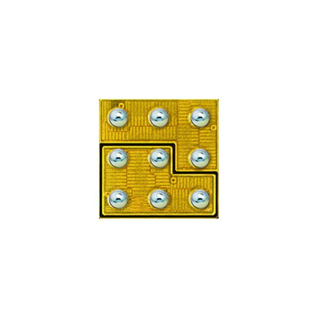
Pad 1 is Gate1 (high side)
Pad 3 is Gate2 (low side)
Pads 4, 7 are VIN
Pads 2, 5, 8 are Switch Node
Pads 6, 9 are Ground
MIN
815 Max
3
DIM
1350
The land pattern is solder mask defined
Solder mask is 10 μm smaller per side than bump
200 +20 / - 10 (*)
(measurements in µm)
X9
4
7
2
5
8
3
6
9
225
450
225
450
1350
450
1
450
* minimum 190
RECOMMENDED
STENCIL DRAWING
1350
Recommended stencil should be 4 mil (100 µm) thick, must be
laser cut, openings per drawing.
250
225
450
450
Intended for use with SAC305 Type 4 solder, reference 88.5%
metals content.
Additional assembly resources available at
https://epc-co.com/epc/DesignSupport/AssemblyBasics.aspx
225
450
1350
450
R6
0
(measurements in µm)
Efficient Power Conversion Corporation (EPC) reserves the right to make changes without further notice to any products herein to
improve reliability, function or design. EPC does not assume any liability arising out of the application or use of any product or circuit
described herein; neither does it convey any license under its patent rights, nor the rights of others.
eGaN® is a registered trademark of Efficient Power Conversion Corporation.
EPC Patent Listing: epc-co.com/epc/AboutEPC/Patents.aspx
EPC – POWER CONVERSION TECHNOLOGY LEADER | EPC-CO.COM | ©2021 |
Information subject to
change without notice.
Revised January, 2021
| 7
�


 工商网监
湘ICP备2023018690号
工商网监
湘ICP备2023018690号
