BCR602 hot plug IC with dimming
60 V linear LED controller IC for dimmable LED applications with ripple suppression,
overtemperature and hot plug protection
Features
•
•
•
•
•
•
Supply voltage 8 V to 60 V,
Supports use of NPN bipolar transistors and NMOS MOSFETS,
AC supply voltage ripple suppression,
Dimming at pin MFIO
- 3% analog dimming of LED current by resistor Rset or DC voltage,
- 1% PWM dimming of LED current by PWM signals,
Rset functionality at pin MFIO,
LED current precision ±3%.
Protection features
•
•
Hot plug protection,
Overtemperature protection.
Target applications
•
•
LED light engines/modules,
LED replacement lamps.
Advantages with respect to discrete solutions
•
•
•
•
Low BOM count,
Lower assembly cost,
Smaller form factor,
Higher reliability due to less parts and soldering joints.
Product validation
Qualified for industrial applications according to the relevant tests of JEDEC47/20/22.
Device information
Figure 1
Datasheet
DRV
1
6
VS
GND
2
5
TEST
VSENSE
3
4
MFIO
Pin configuration
www.infineon.com
Please read the Important Notice and Warnings at the end of this document
Revision 1.1
2018-12-3
�BCR602 hot plug IC with dimming
Description
Table 1
Type
Part information
Package
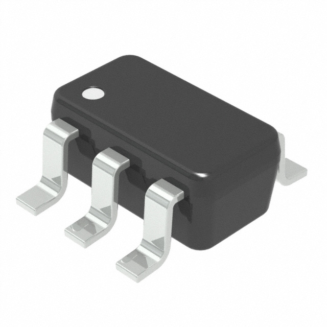
60V Linear Current Control PG-SOT23-6
Chip BCR602
Configuration
Marking code
n.a.
602
Description
BCR602 is a linear LED controller IC regulating the LED current by means of an external driver transistor. BCR602
supports use of NPN bipolar transistors and NMOSFETs to cover a wide LED current and power range up to
several hundred mA. The LED current is fully scalable by dimensioning an external current sense resistor.
BCR602 suppresses the voltage ripple of the power supply driving a constant LED current for better light quality.
The LED current can be dimmed by resistors as well as analog or digital PWM voltages connected to the Multi
Function Input Output (MFIO) pin. The embedded hot plug protection allows plug in and plug out of any LED
load during operation.
The overtemperature protection will dim the LED current if the BCR602 junction temperature threshold is
exceeded. In this case the LED current will be reduced to 30% of the nominal current. Once the junction
temperature drops below the temperature hysteresis nominal LED current is resumed.
The BCR602 is a perfect fit for LED applications by combining small form factor with low cost. Through its higher
integration, BOM savings and ensuring long lifetime of LEDs, this controller has many advantages compared to
discrete solutions.
Datasheet
2
Revision 1.1
2018-12-3
�BCR602 hot plug IC with dimming
Table of contents
Table of contents
Features . . . . . . . . . . . . . . . . . . . . . . . . . . . . . . . . . . . . . . . . . . . . . . . . . . . . . . . . . . . . . . . . . . . . . . . . . . . . . . . 1
Protection features . . . . . . . . . . . . . . . . . . . . . . . . . . . . . . . . . . . . . . . . . . . . . . . . . . . . . . . . . . . . . . . . . . . . . 1
Target applications . . . . . . . . . . . . . . . . . . . . . . . . . . . . . . . . . . . . . . . . . . . . . . . . . . . . . . . . . . . . . . . . . . . . . 1
Advantages with respect to discrete solutions . . . . . . . . . . . . . . . . . . . . . . . . . . . . . . . . . . . . . . . . . . . .1
Product validation . . . . . . . . . . . . . . . . . . . . . . . . . . . . . . . . . . . . . . . . . . . . . . . . . . . . . . . . . . . . . . . . . . . . . .1
Device information . . . . . . . . . . . . . . . . . . . . . . . . . . . . . . . . . . . . . . . . . . . . . . . . . . . . . . . . . . . . . . . . . . . . . 1
Description . . . . . . . . . . . . . . . . . . . . . . . . . . . . . . . . . . . . . . . . . . . . . . . . . . . . . . . . . . . . . . . . . . . . . . . . . . . . .2
Table of contents . . . . . . . . . . . . . . . . . . . . . . . . . . . . . . . . . . . . . . . . . . . . . . . . . . . . . . . . . . . . . . . . . . . . . . . 3
1
Pin configuration . . . . . . . . . . . . . . . . . . . . . . . . . . . . . . . . . . . . . . . . . . . . . . . . . . . . . . . . . . . . . . . . . . . . . . . 4
2
Functional description . . . . . . . . . . . . . . . . . . . . . . . . . . . . . . . . . . . . . . . . . . . . . . . . . . . . . . . . . . . . . . . . . . 5
3
Thermal characteristics . . . . . . . . . . . . . . . . . . . . . . . . . . . . . . . . . . . . . . . . . . . . . . . . . . . . . . . . . . . . . . . . . 7
4
Absolute maximum ratings . . . . . . . . . . . . . . . . . . . . . . . . . . . . . . . . . . . . . . . . . . . . . . . . . . . . . . . . . . . . . .8
5
Operating conditions . . . . . . . . . . . . . . . . . . . . . . . . . . . . . . . . . . . . . . . . . . . . . . . . . . . . . . . . . . . . . . . . . . . 9
6
Electrical characteristics . . . . . . . . . . . . . . . . . . . . . . . . . . . . . . . . . . . . . . . . . . . . . . . . . . . . . . . . . . . . . . . 10
7
Package information . . . . . . . . . . . . . . . . . . . . . . . . . . . . . . . . . . . . . . . . . . . . . . . . . . . . . . . . . . . . . . . . . . 13
8
References . . . . . . . . . . . . . . . . . . . . . . . . . . . . . . . . . . . . . . . . . . . . . . . . . . . . . . . . . . . . . . . . . . . . . . . . . . . . 14
Revision history . . . . . . . . . . . . . . . . . . . . . . . . . . . . . . . . . . . . . . . . . . . . . . . . . . . . . . . . . . . . . . . . . . . . . . . 14
Disclaimer . . . . . . . . . . . . . . . . . . . . . . . . . . . . . . . . . . . . . . . . . . . . . . . . . . . . . . . . . . . . . . . . . . . . . . . . . . . . 15
Datasheet
3
Revision 1.1
2018-12-3
�BCR602 hot plug IC with dimming
Pin configuration
1
Pin configuration
Figure 2
Pin configuration
Table 2
Pin configuration
DRV
1
6
VS
GND
2
5
TEST
VSENSE
3
4
MFIO
Pin no.
Pin name
Pin type
Function
1
DRV
Output
Driver output to control base or gate of the external transistor
2
GND
GND
IC ground
3
VSENSE
Input
Measurement of Vsense voltage
4
MFIO
Input
Multifunctional IO for resistive (via external Rset), DC voltage and
PWM voltage dimming
5
TEST
Output
For test purpose, it must not be directly connected to ground. It is
recommended to leave TEST pin open or attach a resistor to
ground > 1 MΩ.
6
VS
Input
Supply voltage
Datasheet
4
Revision 1.1
2018-12-3
�BCR602 hot plug IC with dimming
Functional description
2
Functional description
Typical application circuit
Cin
Rpred
Controller
IC
OR
VS
DRV
BCR602
GND
VSENSE
Rsense
TEST
MFIO
Rset
DAC
PWM
Figure 3
µC
U
Typical application circuit
Application hints
1.
2.
External driver transistors
BCR602 is able to drive NPN transistors as well as NMOSFETs. NPN transistors can be used for LED
currents up to several 100 mA while NMOSFETs are preferable for high LED currents. The smaller current
using BJTs is caused by the DC current gain value hFE value of the used BJT. E.g. a typical hFE of 75 limits
the application to a maximum below 750 mA.
Supply voltage of BCR602
To drive higher output currents into an external NPN driver transistor it might be necessary to limit the
supply voltage of BCR602 significantly below 60 V to reduce power dissipation inside the IC. This can be
achieved either by adding a series resistor (Rpred) between supply voltage and VS pin of BCR602 or by
operating BCR602 by an auxiliary winding of the power supply providing a lower IC supply voltage as e.g.
8 V or higher.
Dimming mechanism
Application MFIO input signal can be a DC voltage or a pulse width modulated digital signal for dimming of the
LED current.
1.
Pure DC dimming: input voltage VMFIO at pin MFIO. Continuous dimming from 3% dimming level up to
100% is embedded into a 100% ceiling plateau and an hysteresis range to off. Static dimming to a fixed
value can be done via the resistor Rset.
Datasheet
5
Revision 1.1
2018-12-3
�BCR602 hot plug IC with dimming
Functional description
ILED
100%
Analog dimming range
3%
0%
3%
off
dim
0.1V 0.2V
Figure 4
2.
3.
VMFIO
100%
3.3 V
5V
DC dimming
Pure PWM dimming: The PWM duty cycle at pin MFIO defines the dimming level. The PWM voltage
amplitude corresponding to LED on must be in the voltage range specified by VMFIO, 100% and PWM
voltage amplitude corresponding to LED off must be in the voltage range specified by VMFIO, off. The LED
current is PWM modulated according to the PWM input signal.
For resistive dimming using Rset and internal MFIO current, the internal pull-down has to be taken into
account. For proper dimensioning refer to Figure 5 .
5V
BCR602
IMFIO,setcs
MFIO
RMFIO/2
Rset
RMFIO/2
V MFIO = IMFIO, setcs
Rset =
Datasheet
Rset * RMFIO
Rset + RMFIO
V MFIO * RMFIO
IMFIO, setcs * Rset − V MFIO
Figure 5
•
•
Limiter,
Buffer
Rset dimensioning for resistor dimming
RMFIO.typical = 285 kΩ,
IMFIO,setcs,typical = 20 µA.
6
Revision 1.1
2018-12-3
�BCR602 hot plug IC with dimming
Thermal characteristics
3
Thermal characteristics
Figure 6
Maximum permitted effective output source current out of pin DRV into external driver
transistor for a design example of 4 mA DC driver
The maximum permitted effective driver source current shown in Figure 6 can be calculated by following
equation:
IDRV =
T OTP, on, min − T A
−V S
RthJA
VS
⋅ Is
=
T OTP, on, min − T A
− IS
V S ⋅ RthJA
The equation considers the power dissipation caused by the current consumption of the IC itself. If the driver
current exceeds the calculated threshold the lower spec limit of the overtemperature protection will be
exceeded and OTP might be triggered.
TOTP, on, min
Datasheet
The lower spec limit of the overtemperature protection threshold should not be
exceeded to avoid triggering the OTP.
7
Revision 1.1
2018-12-3
�BCR602 hot plug IC with dimming
Absolute maximum ratings
4
Absolute maximum ratings
Table 3
Absolute maximum ratings
Parameter
Symbol
Values
Min.
Typ.
Unit
Note or test condition
Max.
Junction temperature
TJ
-40
–
160
°C
–
Supply voltage
VS
0
–
65
V
–
Input voltage at pin MFIO VMFIO
0
–
5.0
V
–
Input voltage at pin
VSENSE
Vsense
0
–
3.6
V
–
Power dissipation
Ptot
–
–
360
mW
VS = 60 V, IS = 2 mA, IDRV
= -4 mA
ESD robustness
VESD,HBM –
–
2
kV
HBMacc. to JEDEC
JS-001
VESD,CDM -
-
500
V
CDM acc. to JEDEC
JS-002
Attention: Stresses above the maximum values listed here may cause permanent damage to the device.
Exposure to absolute maximum rating conditions for extended periods may affect device
reliability. Maximum ratings are absolute ratings. Exceeding only one of these values may cause
irreversible damage to the integrated circuit.
Table 4
Parameter
Maximum thermal resistance
Symbol
Values
Min.
Thermal resistance
junction to ambient
Datasheet
RthJA
Typ.
Unit
Note or test condition
Max.
–
–
290
K/W
JEDEC 1s0p (JESD
51-3) footprint w/o
extra cooling area
RthJA,100 –
–
200
K/W
JEDEC 1s0p (JESD
51-3) with 100 mm²
cooling area
RthJA,300 –
–
180
K/W
JEDEC 1s0p (JESD
51-3) with 300 mm²
cooling area
8
Revision 1.1
2018-12-3
�BCR602 hot plug IC with dimming
Operating conditions
5
Operating conditions
Table 5
Operating conditions
Parameter
Symbol
Values
Min.
Typ.
Unit
Note or test condition
Max.
Junction temperature
TJ
–40
–
160
°C
–
Supply voltage
VS
0
–
60
V
–
Datasheet
9
Revision 1.1
2018-12-3
�BCR602 hot plug IC with dimming
Electrical characteristics
6
Electrical characteristics
Note:
All parameters are measured at TA = 25°C, VS = 45 V unless otherwise specified.
Note:
ILED,target current is the undimmed current at a VSENSE voltage drop of 400 mV typical.
Table 6
DC characteristics
Parameter
Symbol
Values
Min.
Typ.
Unit
Note or test condition
Max.
IC system
Supply voltage
VS
8
–
60
V
Operational supply
voltage range
Supply voltage brownin
VS,bi
–
–
8
V
–
Supply voltage brownout VS,bo
6.7
–
–
V
–
Supply current
IS
-2.2
–
-
mA
IDRV, source = 0 A
Sense voltage
Vsense
388
400
412
mV
Closed loop reference
voltage of pin VSENSE,
ILED = Vsense / Rsense
–
3
%
Closed loop LED
current accuracy
without dimming at
VMFIO = 3.3 V
10
–
-
mA
Source current range of
pin DRV to drive NPN
base/NMOS gate
LED current accuracy
LED current accuracy
ILED, acc / -3
ILED, acc,
target
Driver
Driver source current
capability, DC
IDRV,
Driver sink current
capability, DC
IDRV, sink
-
–
-10
mA
Sink current range of
pin DRV to discharge
NPN base/NMOS gate
Driver source voltage
VDRV
4.5
5
5.5
V
Max. output voltage of
pin DRV
source
Dimming analog
MFIO turn-off range
VMFIO, off 0
–
0.1
V
Threshold for analog
dimming to off
MFIO turn-on range
VMFIO,on 0.17
–
0.195
V
Threshold for analog
dimming to on
MFIO full current range
VMFIO,
100%
3.3
–
5
V
MFIO range always at
100% ILED
MFIO output source
current
IMFIO,
18
20
22
µA
For RSET < 10 kΩ, in
parallel internal pulldown RMFIO connected,
refer to Figure 5
MFIO output voltage
VMFIO,
–
4.2
–
V
MFIO output voltage at
MFIO open
setcs
setcs
Datasheet
10
Revision 1.1
2018-12-3
�BCR602 hot plug IC with dimming
Electrical characteristics
Table 6
DC characteristics (continued)
Parameter
Symbol
Values
Min.
Typ.
Unit
Note or test condition
Max.
MFIO pull-down resistor
RMFIO
228
285
342
kΩ
Internal pull-down
resistor at pin MFIO
MFIO dimming range
VMFIO,
0.2
–
3.3
V
Analog dimming range
of the LED current
–
3
–
%
Minimum dimming LED
current level at MFIOdim
= 0.15 V
-20
–
20
%
Max variation at
minimum MFIO
dimming level
dim
Analog LED dimming
ILEDmin,
ana /
ILEDmin,
target
LED current chip to chip
variation at selected
dimming level
-10
10
Max variation for
dimming level higher
than minimum
Dimming PWM1)
MFIO PWM frequency
fPWM
–
–
3.5
kHz
Maximum supported
PWM frequency at pin
MFIO, external switch
Qg= 8.7 nC
Minimum PWM duty
cycle
ILEDmin,
PWM /
ILED,
–
1
–
%
Minimum LED current
dimming ratio by a
PWM signal connected
to pin MFIO, external
switch Qg= 8.7 nC
2.9
–
–
µs
Minimum LED PWM
digital pulse width
between 0 V and 3.3 V,
external switch Qg= 8.7
nC
target
Minimum pulse width
tduty, on
Overtemperature protection OTP
Overtemperature
protection threshold,
turn on
TOTP, on
140
–
155
°C
Junction threshold
temperature to trigger
overtemperature
protection in standby,
IDRV = 0 mA and VS = 45
V
Overtemperature
protection threshold,
turn off
TOTP, off
120
–
135
°C
Junction threshold
temperature to exit
overtemperature
protection in standby,
IDRV = 0 mA and VS = 45
V
1
Tested at 0.5 kHz and 3.5 kHz.
Datasheet
11
Revision 1.1
2018-12-3
�BCR602 hot plug IC with dimming
Electrical characteristics
Table 6
DC characteristics (continued)
Parameter
Symbol
Values
Min.
Sense voltage in OTP
case
Vsense,
OTP /
Vsense,
Typ.
Unit
Note or test condition
Max.
–
30
–
%
Reduction factor at pin
VSENSE (nominal 400
mV) if OTP has been
triggered, ILED, OTP =
Vsense,OTP / Rsense
TOTP, Hys –
20
–
°C
–
Vsense, HP –
8
–
mV
VSENSE level at which
hot plug event is
detected
target
Overtemperature
protection hysteresis
Hot plug
Hot plug VSENSE
threshold
Datasheet
12
Revision 1.1
2018-12-3
�BCR602 hot plug IC with dimming
Package information
7
Package information
Dimensions in mm.
1)
1)
0.15 C A-B 2x
1.25±0.2
(0.85)
8°
0°. .
0.2
0.15 C D 2x
+0.075
C
0.1 C
SEATING COPLANARITY
PLANE
0.4±0.1
1.6
0.45±0.1
1
INDEX
MARKING
B
0.2 C 6x
2.8
D
C A B 6x
BOTTOM VIEW
A
6
0.25
GAUGE
PLANE
2.9
0.125-0.045
0.1±0.05
STAND OFF
1.15±0.15
Note:
4
4
6
3
3
1
0.95
1) DOES NOT INCLUDE PLASTIC OR METAL PROTRUSION OF 0.15 MAX. PER SIDE
ALL DIMENSIONS ARE IN UNITS MM
THE DRAWING IS IN COMPLIANCE WITH ISO 128 & PROJECTION METHOD 1 [
Figure 7
Datasheet
]
Package outline PG-SOT23-6
13
Revision 1.1
2018-12-3
�BCR602 hot plug IC with dimming
References
8
References
Revision history
Document
version
Date of
release
Description of changes
v1.0
2018-11-23
•
Public release
v1.1
2018-12-03
•
Parameter update
Datasheet
14
Revision 1.1
2018-12-3
�Trademarks
All referenced product or service names and trademarks are the property of their respective owners.
Edition 2018-12-3
Published by
Infineon Technologies AG
81726 Munich, Germany
© 2018 Infineon Technologies AG
All Rights Reserved.
Do you have a question about any
aspect of this document?
Email: erratum@infineon.com
Document reference
IFX-rjb1519293082418
IMPORTANT NOTICE
The information given in this document shall in no
event be regarded as a guarantee of conditions or
characteristics (“Beschaffenheitsgarantie”) .
With respect to any examples, hints or any typical values
stated herein and/or any information regarding the
application of the product, Infineon Technologies
hereby disclaims any and all warranties and liabilities of
any kind, including without limitation warranties of
non-infringement of intellectual property rights of any
third party.
In addition, any information given in this document is
subject to customer’s compliance with its obligations
stated in this document and any applicable legal
requirements, norms and standards concerning
customer’s products and any use of the product of
Infineon Technologies in customer’s applications.
The data contained in this document is exclusively
intended for technically trained staff. It is the
responsibility of customer’s technical departments to
evaluate the suitability of the product for the intended
application and the completeness of the product
information given in this document with respect to such
application.
WARNINGS
Due to technical requirements products may contain
dangerous substances. For information on the types
in question please contact your nearest Infineon
Technologies office.
Except as otherwise explicitly approved by Infineon
Technologies in a written document signed by
authorized representatives of Infineon Technologies,
Infineon Technologies’ products may not be used in
any applications where a failure of the product or
any consequences of the use thereof can reasonably
be expected to result in personal injury
�


 工商网监
湘ICP备2023018690号
工商网监
湘ICP备2023018690号
