MOSFET
Metal�Oxide�Semiconductor�Field�Effect�Transistor
CoolMOS™�C6��650V�
650V�CoolMOS™�C6�Power�Transistor
IPD65R950C6�
Data�Sheet
Rev.�2.1
Final
Industrial�&�Multimarket
�650V�CoolMOS™�C6�Power�Transistor
IPD65R950C6
1�����Description
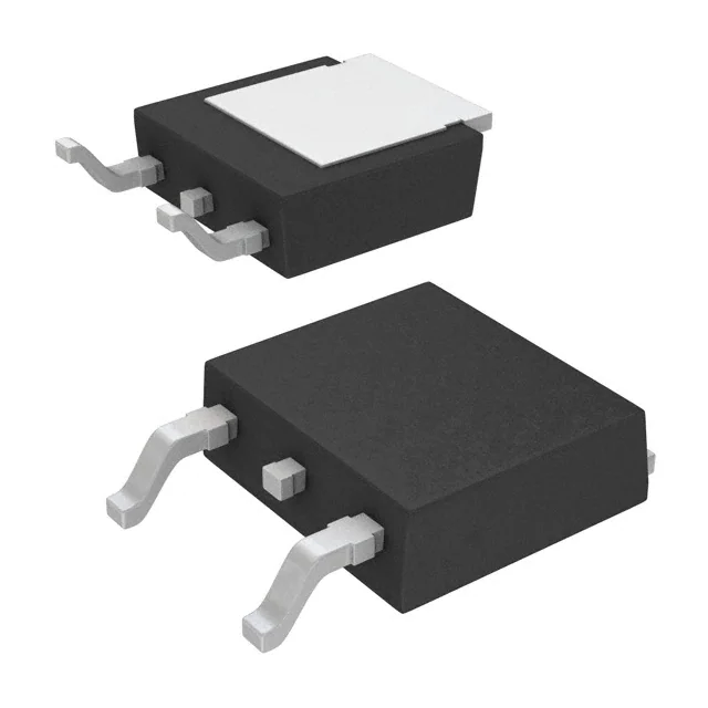
DPAK
CoolMOS™�is�a�revolutionary�technology�for�high�voltage�power
MOSFETs,�designed�according�to�the�superjunction�(SJ)�principle�and
pioneered�by�Infineon�Technologies.�CoolMOS™�C6�series�combines�the
experience�of�the�leading�SJ�MOSFET�supplier�with�high�class�innovation.
The�resulting�devices�provide�all�benefits�of�a�fast�switching�SJ�MOSFET
while�not�sacrificing�ease�of�use.�Extremely�low�switching�and�conduction
losses�make�switching�applications�even�more�efficient,�more�compact,
lighter�and�cooler.
tab
2
1
3
Features
•�Extremely�low�losses�due�to�very�low�FOM�Rdson*Qg�and�Eoss
•�Very�high�commutation�ruggedness
•�Easy�to�use/drive
•�Pb-free�plating,�Halogen�free�mold�compound
•�Fully qualified according to JEDEC for Industrial Applications�
Drain
Pin 2
Gate
Pin 1
Source
Pin 3
Applications
Hard�switching�PWM�stages�and�resonant�switching�PWM�stages�for�e.g.
PC�Silverbox,�Adapter,�LCD�&�PDP�TV�and�Lighting.
Table�1�����Key�Performance�Parameters
Parameter
Value
Unit
VDS @ Tj max
700
V
RDS(on),max
0.95
Ω
Qg,typ
15.3
nC
ID,pulse
12
A
Eoss @ 400V
1.5
µJ
Body diode di/dt
500
A/µs
Type�/�Ordering�Code
Package
Marking
IPD65R950C6
PG-TO 252
65C6950
Final Data Sheet
2
Related�Links
see Appendix A
Rev.�2.1,�2020-05-20
�650V�CoolMOS™�C6�Power�Transistor
IPD65R950C6
Table�of�Contents
Description . . . . . . . . . . . . . . . . . . . . . . . . . . . . . . . . . . . . . . . . . . . . . . . . . . . . . . . . . . . . . . . . . . . . . . . . . . . . . 2
Table of Contents . . . . . . . . . . . . . . . . . . . . . . . . . . . . . . . . . . . . . . . . . . . . . . . . . . . . . . . . . . . . . . . . . . . . . . . . 3
Maximum ratings . . . . . . . . . . . . . . . . . . . . . . . . . . . . . . . . . . . . . . . . . . . . . . . . . . . . . . . . . . . . . . . . . . . . . . . . 4
Thermal characteristics . . . . . . . . . . . . . . . . . . . . . . . . . . . . . . . . . . . . . . . . . . . . . . . . . . . . . . . . . . . . . . . . . . . . 5
Electrical characteristics . . . . . . . . . . . . . . . . . . . . . . . . . . . . . . . . . . . . . . . . . . . . . . . . . . . . . . . . . . . . . . . . . . . 6
Electrical characteristics diagrams . . . . . . . . . . . . . . . . . . . . . . . . . . . . . . . . . . . . . . . . . . . . . . . . . . . . . . . . . . . 8
Test Circuits . . . . . . . . . . . . . . . . . . . . . . . . . . . . . . . . . . . . . . . . . . . . . . . . . . . . . . . . . . . . . . . . . . . . . . . . . . . 12
Package Outlines . . . . . . . . . . . . . . . . . . . . . . . . . . . . . . . . . . . . . . . . . . . . . . . . . . . . . . . . . . . . . . . . . . . . . . . 13
Appendix A . . . . . . . . . . . . . . . . . . . . . . . . . . . . . . . . . . . . . . . . . . . . . . . . . . . . . . . . . . . . . . . . . . . . . . . . . . . . 14
Revision History . . . . . . . . . . . . . . . . . . . . . . . . . . . . . . . . . . . . . . . . . . . . . . . . . . . . . . . . . . . . . . . . . . . . . . . . 15
Disclaimer . . . . . . . . . . . . . . . . . . . . . . . . . . . . . . . . . . . . . . . . . . . . . . . . . . . . . . . . . . . . . . . . . . . . . . . . . . . . 15
Final Data Sheet
3
Rev. 2.1, 2020-05-20
�650V�CoolMOS™�C6�Power�Transistor
IPD65R950C6
2�����Maximum�ratings
at�Tj�=�25°C,�unless�otherwise�specified
Table�2�����Maximum�ratings
Parameter
Symbol
Continuous drain current 1)
I�D
Values
Min.
Typ.
Max.
4.5
Unit
Note�/�Test�Condition
A
TC�=�25°C
TC�=�100°C
2.8
I�D‚pulse
12
A
TC�=�25°C
Avalanche energy, single pulse
EAS
50
mJ
ID�=�1.0A,�VDD�=�50V
(see table 10)
Avalanche energy, repetitive
EAR
0.15
mJ
ID�=�1.0A,�VDD�=�50V
Avalanche current, repetitive
I�AR
1.0
A
MOSFET dv/dt ruggedness
dv/dt
50
V/ns
VDS�=�0�...�480V
Gate source voltage
VGS
-20
20
V
static
-30
30
-55
150
°C
Pulsed drain current
2)
AC (f > 1 Hz)
Operating and storage temperature
Tj‚Tstg
Continuous diode forward current
I�S
3.9
A
TC�=�25°C
Diode pulse current
I�S‚pulse
12
A
TC�=�25°C
Reverse diode dv/dt 3)
dv/dt
15
V/ns
Maximum diode commutation speed
dif/dt
500
A/µs
VDS�=�0�...�400V,�ISD�≤�ID,
Tj�=�25°C
(see table 8)
Power dissipation
Ptot
37
W
TC=25°
1)
Limited by Tj max. Maximum duty cycle D=0.75
Pulse width tp limited by Tj max
3)
Identical low side and high side switch with identical RG
2)
Final Data Sheet
4
Rev. 2.1, 2020-05-20
�650V�CoolMOS™�C6�Power�Transistor
IPD65R950C6
3�����Thermal�characteristics
Table�3�����Thermal�characteristics�DPAK
Parameter
Symbol
Thermal resistance, junction - case
Thermal resistance, junction - ambient
1)
Values
Min.
Typ.
Max.
Unit
RthJC
3.4
°C/W
RthJA
62
°C/W leaded
SMD version, device on PCB,
6cm² cooling area
35
Soldering temperature, wave- &
reflowsoldering allowed
Note�/�Test�Condition
Tsold
260
°C
1.6 mm (0.063 in.) from case for
10s
1)
Device on 40mm*40mm*1.5mm one layer epoxy PCB FR4 with 6cm² copper area (thickness 70µm) for drain connection.
PCB is vertical without air stream cooling.
Final Data Sheet
5
Rev. 2.1, 2020-05-20
�650V�CoolMOS™�C6�Power�Transistor
IPD65R950C6
4�����Electrical�characteristics
at�Tj�=�25°C,�unless�otherwise�specified
Table�4�����Static�characteristics
Values
Parameter
Symbol
Drain-source breakdown voltage
V(BR)DSS
650
Gate threshold voltage
VGS(th)
2.5
Zero gate voltage drain current
I�DSS
Min.
Typ.
3
Unit
Note�/�Test�Condition
V
VGS�=�0V,�ID�=�1mA
3.5
V
VDS�=�VGS,�ID�=�0.2mA
1
µA
VDS�=�650V,�VGS�=�0V,�Tj�=�25°C
Max.
VDS�=�650V,�VGS�=�0V,�Tj�=�150°C
10
Gate-source leakage current
I�GSS
Drain-source on-state resistance
RDS(on)
0.855
100
nA
VGS�=�20V,�VDS�=�0V
0.95
Ω
VGS�=�10V,�ID�=�1.5A,�Tj�=�25°C
VGS�=�10V,�ID�=�1.5A,�Tj�=�150°C
2.223
Gate resistance
RG
5.5
Ω
f�=�1MHz,�open�drain
Unit
Note�/�Test�Condition
VGS�=�0V,�VDS�=�100V,�f�=�1MHz
Table�5�����Dynamic�characteristics
Values
Parameter
Symbol
Input capacitance
Ciss
328
pF
Output capacitance
Coss
23
pF
Effective output capacitance, energy
related 1)
Co(er)
14
pF
VGS�=�0V,�VDS�=�0�...�480V
Effective output capacitance, time related
Co(tr)
58.5
pF
ID�=�constant,�VGS�=�0V,
VDS�=�0�...�480V
Turn-on delay time
td(on)
6.6
ns
Rise time
tr
5.2
ns
Turn-off delay time
td(off)
41
ns
Fall time
tf
13.6
ns
2)
Min.
Typ.
Max.
VDD�=�400V,�VGS�=�13V,�ID�=�2.2A,
RG�=�10.2Ω
(see table 9)
Table�6�����Gate�charge�characteristics
Parameter
Symbol
Gate to source charge
Qgs
Gate to drain charge
Values
Unit
Note�/�Test�Condition
1.8
nC
Qgd
8
nC
VDD�=�480V,�ID�=�2.2A,
VGS�=�0�to�10V
Gate charge total
Qg
15.3
nC
Gate plateau voltage
Vplateau
5.1
V
1)
2)
Min.
Typ.
Max.
Co(er) is a fixed capacitance that gives the same stored energy as Coss while VDS is rising from 0 to 80% V(BR)DSS
Co(tr) is a fixed capacitance that gives the same charging time as Coss while VDS is rising from 0 to 80% V(BR)DSS
Final Data Sheet
6
Rev. 2.1, 2020-05-20
�650V�CoolMOS™�C6�Power�Transistor
IPD65R950C6
Table�7�����Reverse�diode�characteristics
Parameter
Symbol
Diode forward voltage
VSD
Reverse recovery time
Values
Unit
Note�/�Test�Condition
0.9
V
VGS�=�0V,�IF�=�2.2A,�Tj�=�25°C
trr
226
ns
Reverse recovery charge
Qrr
1.3
µC
Peak reverse recovery current
I�rrm
VR�=�400V,�IF�=�2.2A,
diF/dt�=�100A/µs
(see table 8)
9.9
A
Final Data Sheet
Min.
7
Typ.
Max.
Rev. 2.1, 2020-05-20
�650V�CoolMOS™�C6�Power�Transistor
IPD65R950C6
5�����Electrical�characteristics�diagrams
Diagram�1:�Power�dissipation
Diagram�2:�Max.�transient�thermal�impedance
101
40
35
0.5
30
100
20
15
0.2
0.1
ZthJC�[K/W]
Ptot�[W]
25
0.05
10-1
0.02
0.01
single pulse
10
5
0
0
40
80
120
TC�[°C]
10-2
160
10-5
10-4
10-3
Ptot=f(TC)
ZthJC�=f(tP);�parameter:�D=tp/T
Diagram�3:�Safe�operating�area
Diagram�4:�Safe�operating�area
10
2
10-2
tp�[s]
10-1
102
1 µs
101
1 µs
101
10 µs
10 µs
10
ID�[A]
ID�[A]
100 µs
0
1 ms
100 µs
100
1 ms
10 ms
10
10 ms
-1
10-1
DC
DC
10-2
100
101
VDS�[V]
102
103
ID=f(VDS);�VGS>7V;TC=25°C;�D=0;�parameter:�tp
Final Data Sheet
10-2
100
101
VDS�[V]
102
103
ID=f(VDS);�VGS>7V;TC=80°C;�D=0;�parameter:�tp
8
Rev. 2.1, 2020-05-20
�650V�CoolMOS™�C6�Power�Transistor
IPD65R950C6
Diagram�5:�Typ.�output�characteristics
Diagram�6:�Typ.�output�characteristics
16
9
20 V
14
8
10 V
7
12
7V
8V
6
8
ID�[A]
10
ID�[A]
20 V
10 V
8V
7V
6
5
6V
4
3
5.5 V
2
5V
6V
4
5.5 V
2
5V
4.5 V
1
4.5 V
0
0
5
10
15
VDS�[V]
0
20
0
5
10
15
VDS�[V]
ID=f(VDS);�Tj=25�°C;�parameter:�VGS
ID=f(VDS);�Tj=125�°C;�parameter:�VGS
Diagram�7:�Typ.�drain-source�on-state�resistance
Diagram�8:�Drain-source�on-state�resistance
7
20
3
6
2
RDS(on)�[Ω]
RDS(on)�[Ω]
5
4
5V
6V
5.5V
6.5 V
7V
3
typ
98%
1
10 V
2
1
0
1
2
3
4
ID�[A]
5
6
7
8
RDS(on)=f(ID);�Tj=125�°C;�parameter:�VGS
Final Data Sheet
0
-60
-20
20
60
Tj�[°C]
100
140
180
RDS(on)=f(Tj);�ID=1.5�A;�VGS=10�V
9
Rev. 2.1, 2020-05-20
�650V�CoolMOS™�C6�Power�Transistor
IPD65R950C6
Diagram�9:�Typ.�transfer�characteristics
Diagram�10:�Typ.�gate�charge
14
10
25 °C
9
12
8
10
480 V
6
VGS�[V]
8
ID�[A]
120 V
7
150 °C
6
5
4
3
4
2
2
0
1
0
2
4
VGS�[V]
6
8
0
10
0
4
8
12
Qgate�[nC]
ID=f(VGS);�VDS�=�20V;�parameter:�Tj
VGS=f(Qgate);�ID=1.5�A�pulsed;�parameter:�VDD
Diagram�11:�Avalanche�energy
Diagram�12:�Drain-source�breakdown�voltage
60
16
750
725
50
700
675
VBR(DSS)�[V]
EAS�[mJ]
40
30
20
650
625
600
10
0
575
0
50
100
Tj�[°C]
150
200
EAS=f(Tj);�ID=1.0�A;�VDD=50�V
Final Data Sheet
550
-60
-20
20
60
Tj�[°C]
100
140
180
VBR(DSS)=f(Tj);�ID=1.0�mA
10
Rev. 2.1, 2020-05-20
�650V�CoolMOS™�C6�Power�Transistor
IPD65R950C6
Diagram�13:�Typ.�capacitances
Diagram�14:�Typ.�Coss�stored�energy
104
2.00
1.80
1.60
103
1.40
Ciss
Eoss�[µJ]
C�[pF]
1.20
102
1.00
0.80
Coss
0.60
101
0.40
Crss
100
0
100
200
0.20
300
VDS�[V]
400
500
600
C=f(VDS);�VGS=0�V;�f=1�MHz
0.00
0
100
200
300
VDS�[V]
400
500
600
Eoss=f(VDS)
Diagram�15:�Forward�characteristics�of�reverse�diode
IF�[A]
101
125 °C
25 °C
100
10-1
0.0
0.5
1.0
VSD�[V]
1.5
2.0
IF=f(VSD);�parameter:�Tj
Final Data Sheet
11
Rev. 2.1, 2020-05-20
�650V�CoolMOS™�C6�Power�Transistor
IPD65R950C6
6�����Test�Circuits
Table�8�����Diode�characteristics
Test circuit for diode characteristics
Diode recovery waveform
V ,I
Rg1
VDS( peak)
VDS
VDS
VDS
trr
IF
Rg 2
tF
tS
dIF / dt
QF
IF
t
dIrr / dt trr =tF +tS
Qrr = QF + QS
Irrm
Rg1 = Rg 2
IF
10 %Irrm
QS
Table�9�����Switching�times
Switching times test circuit for inductive load
Switching times waveform
VDS
90%
VDS
VGS
VGS
10%
td(on)
td(off)
tr
ton
tf
toff
Table�10�����Unclamped�inductive�load
Unclamped inductive load test circuit
Unclamped inductive waveform
V(BR)DS
ID
VD
VDS
VDS
Final Data Sheet
12
ID
VDS
Rev. 2.1, 2020-05-20
�650V�CoolMOS™�C6�Power�Transistor
IPD65R950C6
7�����Package�Outlines
DIMENSION
A
A1
b
b2
b3
c
c2
D
D1
E
E1
e
e1
N
H
L
L3
L4
MILLIMETERS
MIN.
MAX.
2.16
2.41
0.00
0.15
0.64
0.89
0.65
1.15
4,95
5.50
0.46
0.61
0.40
0.98
5.97
6.22
5.84
5.02
6.35
6.73
4.32
5.50
2.29
4.57
3
10.48
9.40
1.18
1.78
1.27
0.89
0.51
1.02
DOCUMENT NO.
Z8B00003328
REVISION
07
SCALE:
10:1
0
2mm
1
EUROPEAN PROJECTION
ISSUE DATE
01.04.2020
Figure�1�����Outline�PG-TO�252,�dimensions�in�mm
Final Data Sheet
13
Rev. 2.1, 2020-05-20
�650V�CoolMOS™�C6�Power�Transistor
IPD65R950C6
8�����Appendix�A
Table�11�����Related�Links
• IFX�C6�Product�Brief:�www.infineon.com
• IFX�C6�Portfolio:�www.infineon.com
• IFX�CoolMOS�Webpage:�www.infineon.com
• IFX�Design�Tools:�www.infineon.com
Final Data Sheet
14
Rev. 2.1, 2020-05-20
�650V�CoolMOSª�C6�Power�Transistor
IPD65R950C6�
Revision�History
IPD65R950C6
Revision:�2020-05-20,�Rev.�2.1
Previous Revision
Revision
Date
Subjects (major changes since last revision)
2.0
2013-07-26
Release of final version
2.1
2020-05-20
Update of the package outlines
Trademarks
All�referenced�product�or�service�names�and�trademarks�are�the�property�of�their�respective�owners.
We�Listen�to�Your�Comments
Any�information�within�this�document�that�you�feel�is�wrong,�unclear�or�missing�at�all?�Your�feedback�will�help�us�to�continuously
improve�the�quality�of�this�document.�Please�send�your�proposal�(including�a�reference�to�this�document)�to:
erratum@infineon.com
Published�by
Infineon�Technologies�AG
81726�München,�Germany
©�2020�Infineon�Technologies�AG
All�Rights�Reserved.
Legal�Disclaimer
The�information�given�in�this�document�shall�in�no�event�be�regarded�as�a�guarantee�of�conditions�or�characteristics�
(“Beschaffenheitsgarantie”)�.
With�respect�to�any�examples,�hints�or�any�typical�values�stated�herein�and/or�any�information�regarding�the�application�of�the
product,�Infineon�Technologies�hereby�disclaims�any�and�all�warranties�and�liabilities�of�any�kind,�including�without�limitation
warranties�of�non-infringement�of�intellectual�property�rights�of�any�third�party.
In�addition,�any�information�given�in�this�document�is�subject�to�customer’s�compliance�with�its�obligations�stated�in�this
document�and�any�applicable�legal�requirements,�norms�and�standards�concerning�customer’s�products�and�any�use�of�the
product�of�Infineon�Technologies�in�customer’s�applications.
The�data�contained�in�this�document�is�exclusively�intended�for�technically�trained�staff.�It�is�the�responsibility�of�customer’s
technical�departments�to�evaluate�the�suitability�of�the�product�for�the�intended�application�and�the�completeness�of�the�product
information�given�in�this�document�with�respect�to�such�application.
Information
For�further�information�on�technology,�delivery�terms�and�conditions�and�prices�please�contact�your�nearest�Infineon
Technologies�Office�(www.infineon.com).
Warnings
Due�to�technical�requirements,�components�may�contain�dangerous�substances.�For�information�on�the�types�in�question,
please�contact�the�nearest�Infineon�Technologies�Office.
The�Infineon�Technologies�component�described�in�this�Data�Sheet�may�be�used�in�life-support�devices�or�systems�and/or
automotive,�aviation�and�aerospace�applications�or�systems�only�with�the�express�written�approval�of�Infineon�Technologies,�if�a
failure�of�such�components�can�reasonably�be�expected�to�cause�the�failure�of�that�life-support,�automotive,�aviation�and
aerospace�device�or�system�or�to�affect�the�safety�or�effectiveness�of�that�device�or�system.�Life�support�devices�or�systems�are
intended�to�be�implanted�in�the�human�body�or�to�support�and/or�maintain�and�sustain�and/or�protect�human�life.�If�they�fail,�it�is
reasonable�to�assume�that�the�health�of�the�user�or�other�persons�may�be�endangered.
15
Rev.�2.1,��2020-05-20
�


 工商网监
湘ICP备2023018690号
工商网监
湘ICP备2023018690号
