IRF3805S-7PPbF
IRF3805L-7PPbF
Features
HEXFET® Power MOSFET
Advanced Process Technology
Ultra Low On-Resistance
175°C Operating Temperature
Fast Switching
Repetitive Avalanche Allowed up to Tjmax
Lead-Free
l
l
l
l
l
l
D
VDSS = 55V
RDS(on) = 2.6mΩ
G
ID = 160A
S
Description
This HEXFET® Power MOSFET utilizes the latest
processing techniques to achieve extremely low
on-resistance per silicon area. Additional features
of this design are a 175°C junction operating
temperature, fast switching speed and improved
repetitive avalanche rating . These features
combine to make this design an extremely efficient
and reliable device for use in a wide variety of
applications.
S (Pin 2, 3, 5, 6, 7)
G (Pin 1)
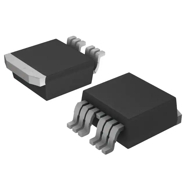
D2Pak 7 Pin
IRF3805S-7PPbF
TO-263CA 7 Pin
IRF3805L-7PPbF
Absolute Maximum Ratings
Parameter
Max.
Units
ID @ TC = 25°C
Continuous Drain Current, VGS @ 10V (Silicon Limited)
240
A
ID @ TC = 100°C
Continuous Drain Current, VGS @ 10V (See Fig. 9)
170
ID @ TC = 25°C
Continuous Drain Current, VGS @ 10V (Package Limited)
160
IDM
Pulsed Drain Current
1000
PD @TC = 25°C
Maximum Power Dissipation
300
W
Linear Derating Factor
2.0
± 20
W/°C
V
440
mJ
c
VGS
EAS
Gate-to-Source Voltage
EAS (tested)
Single Pulse Avalanche Energy Tested Value
Single Pulse Avalanche Energy (Thermally Limited)
c
IAR
Avalanche Current
EAR
Repetitive Avalanche Energy
TJ
Operating Junction and
TSTG
Storage Temperature Range
h
d
g
300 (1.6mm from case )
10 lbf•in (1.1N•m)
Thermal Resistance
j
Parameter
RθCS
Case-to-Sink, Flat, Greased Surface
RθJA
Junction-to-Ambient
RθJA
Junction-to-Ambient (PCB Mount, steady state)
j
A
°C
-55 to + 175
Mounting torque, 6-32 or M3 screw
Junction-to-Case
See Fig.12a,12b,15,16
mJ
Soldering Temperature, for 10 seconds
RθJC
680
ij
Typ.
Max.
Units
–––
0.50
°C/W
0.50
–––
–––
62
–––
40
HEXFET® is a registered trademark of International Rectifier.
1 www.irf.com © 2013 International Rectifier Submit Datasheet Feedback October 25, 2013
�IRF3805S/L-7PPbF
Static @ TJ = 25°C (unless otherwise specified)
Parameter
V(BR)DSS
∆ΒVDSS/∆TJ
RDS(on) SMD
VGS(th)
Drain-to-Source Breakdown Voltage
Breakdown Voltage Temp. Coefficient
Static Drain-to-Source On-Resistance
Gate Threshold Voltage
gfs
IDSS
Forward Transconductance
Drain-to-Source Leakage Current
IGSS
Min. Typ. Max. Units
–––
0.05
–––
–––
Qg
Qgs
Qgd
td(on)
tr
td(off)
tf
LD
Gate-to-Source Forward Leakage
Gate-to-Source Reverse Leakage
Total Gate Charge
Gate-to-Source Charge
Gate-to-Drain ("Miller") Charge
Turn-On Delay Time
Rise Time
Turn-Off Delay Time
Fall Time
Internal Drain Inductance
55
–––
–––
2.0
110
–––
–––
–––
–––
–––
–––
–––
–––
–––
–––
–––
–––
2.0
–––
–––
–––
–––
–––
–––
130
53
49
23
130
80
52
4.5
2.6
4.0
–––
20
250
200
-200
200
–––
–––
–––
–––
–––
–––
–––
LS
Internal Source Inductance
–––
7.5
–––
Ciss
Coss
Crss
Coss
Coss
Coss eff.
Input Capacitance
Output Capacitance
Reverse Transfer Capacitance
Output Capacitance
Output Capacitance
Effective Output Capacitance
–––
–––
–––
–––
–––
–––
7820
1260
610
4310
980
1540
–––
–––
–––
–––
–––
–––
Conditions
V VGS = 0V, ID = 250µA
V/°C Reference to 25°C, ID = 1mA
mΩ VGS = 10V, ID = 140A
V VDS = VGS, ID = 250µA
S VDS = 25V, ID = 140A
µA VDS = 55V, VGS = 0V
VDS = 55V, VGS = 0V, TJ = 125°C
nA VGS = 20V
VGS = -20V
nC ID = 140A
VDS = 44V
VGS = 10V
ns VDD = 28V
ID = 140A
RG = 2.4Ω
VGS = 10V
D
nH Between lead,
e
e
d
6mm (0.25in.)
from package
pF
G
S
and center of die contact
VGS = 0V
VDS = 25V
ƒ = 1.0MHz, See Fig. 5
VGS = 0V, VDS = 1.0V, ƒ = 1.0MHz
VGS = 0V, VDS = 44V, ƒ = 1.0MHz
VGS = 0V, VDS = 0V to 44V
Diode Characteristics
Parameter
Min. Typ. Max. Units
IS
Continuous Source Current
–––
–––
240
ISM
(Body Diode)
Pulsed Source Current
–––
–––
1000
VSD
trr
Qrr
Diode Forward Voltage
Reverse Recovery Time
Reverse Recovery Charge
–––
–––
–––
–––
45
35
1.3
68
53
(Body Diode)�c
A
Notes:
Repetitive rating; pulse width limited by
max. junction temperature. (See fig. 11).
Limited by TJmax, starting TJ = 25°C,
L=0.043mH, R G = 25Ω, IAS = 140A, VGS =10V.
Part not recommended for use above this value.
Pulse width ≤ 1.0ms; duty cycle ≤ 2%.
Coss eff. is a fixed capacitance that gives the same
charging time as Coss while VDS is rising from 0 to 80%
VDSS.
Conditions
MOSFET symbol
V
ns
nC
showing the
integral reverse
D
G
S
p-n junction diode.
TJ = 25°C, IS = 140A, VGS = 0V
TJ = 25°C, IF = 140A, VDD = 28V
di/dt = 100A/µs
e
e
Limited by TJmax , see Fig.12a, 12b, 15, 16 for typical repetitive
avalanche performance.
This value determined from sample failure population. 100%
tested to this value in production.
This is applied to D2Pak, when mounted on 1" square PCB
( FR-4 or G-10 Material ). For recommended footprint and
soldering techniques refer to application note #AN-994.
Rθ is measured at TJ of approximately 90°C.
Solder mounted on IMS substrate.
2 www.irf.com © 2013 International Rectifier Submit Datasheet Feedback October 25, 2013
�IRF3805S/L-7PPbF
10000
10000
1000
BOTTOM
100
VGS
15V
10V
8.0V
7.0V
6.0V
5.5V
5.0V
4.5V
TOP
ID, Drain-to-Source Current (A)
ID, Drain-to-Source Current (A)
TOP
1000
10
1
4.5V
BOTTOM
100
4.5V
10
≤60µs PULSE WIDTH
≤60µs PULSE WIDTH
Tj = 175°C
Tj = 25°C
0.1
0.1
1
10
1
100
1000
0.1
V DS, Drain-to-Source Voltage (V)
1
10
100
1000
V DS, Drain-to-Source Voltage (V)
Fig 1. Typical Output Characteristics
Fig 2. Typical Output Characteristics
1000
250
Gfs, Forward Transconductance (S)
ID, Drain-to-Source Current (Α)
VGS
15V
10V
8.0V
7.0V
6.0V
5.5V
5.0V
4.5V
T J = 175°C
100
TJ = 25°C
10
VDS = 25V
≤60µs PULSE WIDTH
1.0
TJ = 25°C
200
150
T J = 175°C
100
50
V DS = 10V
380µs PULSE WIDTH
0
2
4
6
8
VGS, Gate-to-Source Voltage (V)
Fig 3. Typical Transfer Characteristics
10
0
20
40
60
80
100
120
ID,Drain-to-Source Current (A)
Fig 4. Typical Forward Transconductance
vs. Drain Current
3 www.irf.com © 2013 International Rectifier Submit Datasheet Feedback October 25, 2013
�IRF3805S/L-7PPbF
100000
12.0
VGS = 0V,
f = 1 MHZ
C iss = C gs + C gd, C ds SHORTED
ID= 140A
VGS, Gate-to-Source Voltage (V)
C rss = C gd
C, Capacitance(pF)
C oss = C ds + C gd
10000
Ciss
Coss
Crss
1000
100
VDS= 64V
VDS= 40V
10.0
8.0
6.0
4.0
2.0
0.0
1
10
100
0
VDS, Drain-to-Source Voltage (V)
50
100
150
QG Total Gate Charge (nC)
Fig 6. Typical Gate Charge vs.
Gate-to-Source Voltage
Fig 5. Typical Capacitance vs.
Drain-to-Source Voltage
10000
10000
1000
T J = 175°C
100
10
T J = 25°C
1
ID, Drain-to-Source Current (A)
ISD, Reverse Drain Current (A)
OPERATION IN THIS AREA
LIMITED BY R DS(on)
1000
1msec 100µsec
100
10
10msec
1
Tc = 25°C
Tj = 175°C
Single Pulse
VGS = 0V
0.1
0.0 0.2 0.4 0.6 0.8 1.0 1.2 1.4 1.6 1.8
VSD, Source-to-Drain Voltage (V)
Fig 7. Typical Source-Drain Diode
Forward Voltage
DC
0.1
0.1
1
10
100
VDS, Drain-to-Source Voltage (V)
Fig 8. Maximum Safe Operating Area
4 www.irf.com © 2013 International Rectifier Submit Datasheet Feedback October 25, 2013
�IRF3805S/L-7PPbF
2.5
Limited By Package
200
ID, Drain Current (A)
RDS(on) , Drain-to-Source On Resistance
(Normalized)
250
150
100
50
ID = 140A
VGS = 10V
2.0
1.5
1.0
0.5
0
25
50
75
100
125
150
-60 -40 -20 0 20 40 60 80 100120140160180
175
T J , Junction Temperature (°C)
T C , Case Temperature (°C)
Fig 10. Normalized On-Resistance
vs. Temperature
Fig 9. Maximum Drain Current vs.
Case Temperature
Thermal Response ( Z thJC )
1
D = 0.50
0.20
0.1
0.10
0.05
τJ
0.02
0.01
0.01
SINGLE PULSE
( THERMAL RESPONSE )
R1
R1
τJ
τ1
τ1
R2
R2
τ2
τ2
Ci= τi/Ri
Ci i/Ri
R3
R3
τ3
τC
τ
τ3
Ri (°C/W)
0.0794
τi (sec)
0.000192
0.1474
0.2737
0.000628
0.014012
Notes:
1. Duty Factor D = t1/t2
2. Peak Tj = P dm x Zthjc + Tc
0.001
1E-005
0.0001
0.001
0.01
0.1
1
t1 , Rectangular Pulse Duration (sec)
Fig 11. Maximum Effective Transient Thermal Impedance, Junction-to-Case
5 www.irf.com © 2013 International Rectifier Submit Datasheet Feedback October 25, 2013
�IRF3805S/L-7PPbF
15V
VDS
D.U.T
RG
VGS
20V
+
V
- DD
IAS
A
0.01Ω
tp
Fig 12a. Unclamped Inductive Test Circuit
V(BR)DSS
tp
EAS , Single Pulse Avalanche Energy (mJ)
2000
DRIVER
L
ID
TOP
21A
37A
BOTTOM 140A
1500
1000
500
0
25
50
75
100
125
150
175
Starting T J , Junction Temperature (°C)
I AS
Fig 12c. Maximum Avalanche Energy
vs. Drain Current
Fig 12b. Unclamped Inductive Waveforms
QG
10 V
QGS
QGD
5.0
Charge
Fig 13a. Basic Gate Charge Waveform
Current Regulator
Same Type as D.U.T.
50KΩ
12V
.2µF
.3µF
D.U.T.
+
V
- DS
VGS(th) Gate threshold Voltage (V)
VG
4.5
4.0
3.5
3.0
2.5
ID = 250µA
ID = 1.0mA
ID = 1.0A
2.0
1.5
-75 -50 -25
VGS
0
25
50
75 100 125 150 175 200
T J , Temperature ( °C )
3mA
IG
ID
Current Sampling Resistors
Fig 13b. Gate Charge Test Circuit
Fig 14. Threshold Voltage vs. Temperature
6 www.irf.com © 2013 International Rectifier Submit Datasheet Feedback October 25, 2013
�IRF3805S/L-7PPbF
1000
Avalanche Current (A)
Duty Cycle = Single Pulse
Allowed avalanche Current vs avalanche
pulsewidth, tav, assuming ∆ Tj = 150°C and
Tstart =25°C (Single Pulse)
100
0.01
0.05
0.10
10
Allowed avalanche Current vs avalanche
pulsewidth, tav, assuming ∆Τ j = 25°C and
Tstart = 150°C.
1
1.0E-06
1.0E-05
1.0E-04
1.0E-03
1.0E-02
1.0E-01
tav (sec)
Fig 15. Typical Avalanche Current vs.Pulsewidth
EAR , Avalanche Energy (mJ)
500
TOP
Single Pulse
BOTTOM 1% Duty Cycle
ID = 140A
400
300
200
100
0
25
50
75
100
125
150
Starting T J , Junction Temperature (°C)
Fig 16. Maximum Avalanche Energy
vs. Temperature
175
Notes on Repetitive Avalanche Curves , Figures 15, 16:
(For further info, see AN-1005 at www.irf.com)
1. Avalanche failures assumption:
Purely a thermal phenomenon and failure occurs at a
temperature far in excess of T jmax. This is validated for
every part type.
2. Safe operation in Avalanche is allowed as long asT jmax is
not exceeded.
3. Equation below based on circuit and waveforms shown in
Figures 12a, 12b.
4. PD (ave) = Average power dissipation per single
avalanche pulse.
5. BV = Rated breakdown voltage (1.3 factor accounts for
voltage increase during avalanche).
6. Iav = Allowable avalanche current.
7. ∆T = Allowable rise in junction temperature, not to exceed
Tjmax (assumed as 25°C in Figure 15, 16).
tav = Average time in avalanche.
D = Duty cycle in avalanche = tav ·f
ZthJC(D, tav ) = Transient thermal resistance, see figure 11)
PD (ave) = 1/2 ( 1.3·BV·Iav) = DT/ ZthJC
Iav = 2DT/ [1.3·BV·Zth]
EAS (AR) = PD (ave)·tav
7 www.irf.com © 2013 International Rectifier Submit Datasheet Feedback October 25, 2013
�IRF3805S/L-7PPbF
D.U.T
Driver Gate Drive
+
-
P.W.
+
D.U.T. ISD Waveform
Reverse
Recovery
Current
+
V DD
• dv/dt controlled by RG
• Driver same type as D.U.T.
• I SD controlled by Duty Factor "D"
• D.U.T. - Device Under Test
P.W.
Period
*
RG
D=
VGS=10V
Circuit Layout Considerations
• Low Stray Inductance
• Ground Plane
• Low Leakage Inductance
Current Transformer
-
Period
+
Body Diode Forward
Current
di/dt
D.U.T. VDS Waveform
Diode Recovery
dv/dt
Re-Applied
Voltage
-
Body Diode
VDD
Forward Drop
Inductor Curent
Ripple ≤ 5%
*
ISD
VGS = 5V for Logic Level Devices
Fig 17. Peak Diode Recovery dv/dt Test Circuit for N-Channel
HEXFET® Power MOSFETs
V DS
V GS
RG
RD
D.U.T.
+
-V DD
10V
Pulse Width ≤ 1 µs
Duty Factor ≤ 0.1 %
Fig 18a. Switching Time Test Circuit
VDS
90%
10%
VGS
td(on)
tr
t d(off)
tf
Fig 18b. Switching Time Waveforms
8 www.irf.com © 2013 International Rectifier Submit Datasheet Feedback October 25, 2013
�IRF3805S/L-7PPbF
D2Pak - 7 Pin Package Outline
Dimensions are shown in millimeters (inches)
Notes:
1. For an Automotive Qualified version of this part please see http://www.irf.com/product-info/auto/
2. For the most current drawing please refer to IR website at http://www.irf.com/package/
9 www.irf.com © 2013 International Rectifier Submit Datasheet Feedback October 25, 2013
�IRF3805S/L-7PPbF
D2Pak - 7 Pin Part Marking Information
�14
D2Pak - 7 Pin Tape and Reel
Notes:
1. For an Automotive Qualified version of this part please see http://www.irf.com/product-info/auto/
2. For the most current drawing please refer to IR website at http://www.irf.com/package/
10 www.irf.com © 2013 International Rectifier Submit Datasheet Feedback October 25, 2013
�IRF3805S/L-7PPbF
TO-263CA 7 Pin Long Leads Package Outline
Dimensions are shown in millimeters (inches)
Notes:
1. For an Automotive Qualified version of this part please see http://www.irf.com/product-info/auto/
2. For the most current drawing please refer to IR website at http://www.irf.com/package/
Revision History
Date
10/25/2013
Comments
•�Remove the "Automotive MOSFET" on the header, on page 1.
IR WORLD HEADQUARTERS: 101 N. Sepulveda Blvd., El Segundo, California 90245, USA
To contact International Rectifier, please visit http://www.irf.com/whoto-call/
11 www.irf.com © 2013 International Rectifier Submit Datasheet Feedback October 25, 2013
�IMPORTANT NOTICE
The information given in this document shall in no
event be regarded as a guarantee of conditions or
characteristics (“Beschaffenheitsgarantie”) .
With respect to any examples, hints or any typical
values stated herein and/or any information
regarding the application of the product, Infineon
Technologies hereby disclaims any and all
warranties and liabilities of any kind, including
without limitation warranties of non-infringement
of intellectual property rights of any third party.
In addition, any information given in this document
is subject to customer’s compliance with its
obligations stated in this document and any
applicable legal requirements, norms and
standards concerning customer’s products and any
use of the product of Infineon Technologies in
customer’s applications.
The data contained in this document is exclusively
intended for technically trained staff. It is the
responsibility of customer’s technical departments
to evaluate the suitability of the product for the
intended application and the completeness of the
product information given in this document with
respect to such application.
For further information on the product, technology,
delivery terms and conditions and prices please
contact your nearest Infineon Technologies office
(www.infineon.com).
WARNINGS
Due to technical requirements products may
contain dangerous substances. For information on
the types in question please contact your nearest
Infineon Technologies office.
Except as otherwise explicitly approved by Infineon
Technologies in a written document signed by
authorized
representatives
of
Infineon
Technologies, Infineon Technologies’ products may
not be used in any applications where a failure of
the product or any consequences of the use thereof
can reasonably be expected to result in personal
injury.
�


 工商网监
湘ICP备2023018690号
工商网监
湘ICP备2023018690号
