END OF LIFE
IRF7380QPbF
l
l
l
l
l
l
l
HEXFET® Power MOSFET
Advanced Process Technology
Ultra Low On-Resistance
N Channel MOSFET
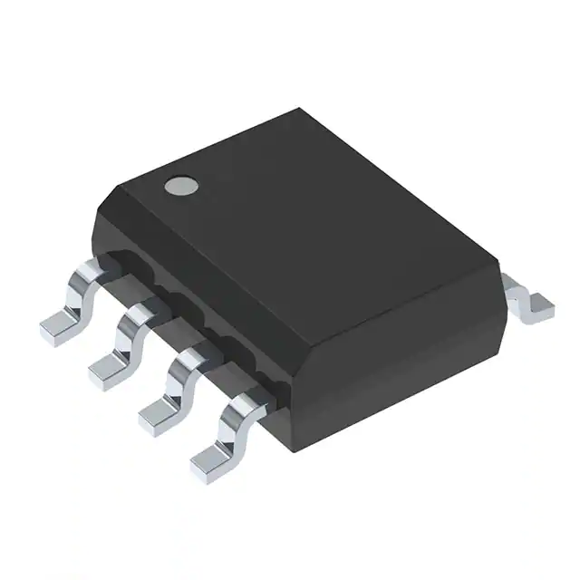
Surface Mount
Available in Tape & Reel
150°C Operating Temperature
Lead-Free
VDSS
80V
Description
Additional features of These HEXFET Power
MOSFET's are a 150°C junction operating temperature,
fast switching speed and improved repetitive avalanche
rating. These benefits combine to make this design an
extremely efficient and reliable device for use in a wide
variety of applications.
The efficient SO-8 package provides enhanced thermal
characteristics making it ideal in a variety of power
applications. This surface mount SO-8 can dramatically
reduce board space and is also available in Tape &
Reel.
IRF7380QPbF
S1
1
8
D1
G1
2
7
D1
S2
3
6
D2
G2
4
5
D2
Standard Pack
Form
Quantity
IRF7380QTRPbF
SO-8
Tape and Reel
IRF7380QPbF
SO-8
Tube
ID
2.2A
SO-8
Top View
Package
Type
Base part number Orderable part number
RDS(on) max
73m:@VGS = 10V
EOL Notice
Replacement Part Number
4000
EOL 529
95
EOL 529
Please search the EOL part number on IR’s
website for guidance
Absolute Maximum Ratings
Parameter
Max.
Units
80
V
VDS
Drain-to-Source Voltage
VGS
ID @ TA = 25°C
Gate-to-Source Voltage
Continuous Drain Current, VGS @ 10V
± 20
3.6
ID @ TA = 100°C
Continuous Drain Current, VGS @ 10V
2.9
IDM
Pulsed Drain Current
29
PD @TA = 25°C
c
Maximum Power Dissipation
Linear Derating Factor
h
dv/dt
TJ
Peak Diode Recovery dv/dt
Operating Junction and
TSTG
Storage Temperature Range
A
2.0
W
0.02
W/°C
2.3
-55 to + 150
V/ns
°C
Thermal Resistance
Parameter
R θJL
Junction-to-Drain Lead
R θJA
Junction-to-Ambient (PCB Mount)
f
Typ.
Max.
Units
–––
42
°C/W
–––
62.5
Notes through are on page 8
1
www.irf.com © 2014 International Rectifier Submit Datasheet Feedback
September 8, 2014
�END OF LIFE
IRF7380QPbF
Static @ TJ = 25°C (unless otherwise specified)
Parameter
Min. Typ. Max. Units
Conditions
V(BR)DSS
Drain-to-Source Breakdown Voltage
80
–––
–––
ΔV(BR)DSS/ΔTJ
Breakdown Voltage Temp. Coefficient
–––
0.09
–––
RDS(on)
Static Drain-to-Source On-Resistance
–––
61
73
VGS(th)
Gate Threshold Voltage
2.0
–––
4.0
V
VDS = VGS, ID = 250μA
IDSS
Drain-to-Source Leakage Current
–––
–––
20
μA
VDS = 80V, VGS = 0V
–––
–––
250
IGSS
Gate-to-Source Forward Leakage
–––
–––
200
nA
VGS = 20V
Gate-to-Source Reverse Leakage
–––
–––
-200
V
VGS = 0V, ID = 250μA
V/°C Reference to 25°C, ID = 1mA
mΩ VGS = 10V, ID = 2.2A
f
VDS = 64V, VGS = 0V, TJ = 125°C
VGS = -20V
Dynamic @ TJ = 25°C (unless otherwise specified)
Parameter
Min. Typ. Max. Units
–––
–––
S
Conditions
gfs
Qg
Forward Transconductance
4.3
VDS = 25V, ID = 2.2A
Total Gate Charge
–––
15
23
Qgs
Gate-to-Source Charge
–––
2.9
–––
Qgd
Gate-to-Drain ("Miller") Charge
–––
4.5
–––
VGS = 10V
td(on)
Turn-On Delay Time
–––
9.0
–––
VDD = 40V
tr
Rise Time
–––
10
–––
td(off)
Turn-Off Delay Time
–––
41
–––
tf
Fall Time
–––
17
–––
VGS = 10V
Ciss
Input Capacitance
–––
660
–––
VGS = 0V
Coss
Output Capacitance
–––
110
–––
Crss
Reverse Transfer Capacitance
–––
15
–––
Coss
Output Capacitance
–––
710
–––
VGS = 0V, VDS = 1.0V, ƒ = 1.0MHz
Coss
Output Capacitance
–––
72
–––
VGS = 0V, VDS = 64V, ƒ = 1.0MHz
Coss eff.
Effective Output Capacitance
–––
140
–––
VGS = 0V, VDS = 0V to 64V
ID = 2.2A
nC
VDS = 40V
f
ID = 2.2A
ns
RG = 24Ω
f
VDS = 25V
pF
ƒ = 1.0MHz
g
Avalanche Characteristics
EAS
Parameter
Single Pulse Avalanche Energy
IAR
Avalanche Current
�c
dh
Typ.
Max.
Units
–––
75
mJ
–––
2.2
A
Diode Characteristics
Parameter
Min. Typ. Max. Units
Conditions
IS
Continuous Source Current
–––
–––
3.6
A
MOSFET symbol
ISM
(Body Diode)
Pulsed Source Current
–––
–––
29
A
showing the
integral reverse
VSD
(Body Diode)
Diode Forward Voltage
–––
–––
1.3
V
p-n junction diode.
TJ = 25°C, IS = 2.2A, VGS = 0V
trr
Reverse Recovery Time
–––
50
–––
ns
Qrr
Reverse Recovery Charge
–––
110
–––
nC
ton
Forward Turn-On Time
�ch
2
D
G
S
f
TJ = 25°C, IF = 2.2A, VDD = 40V
di/dt = 100A/μs
f
Intrinsic turn-on time is negligible (turn-on is dominated by LS+LD)
www.irf.com © 2014 International Rectifier Submit Datasheet Feedback
September 8, 2014
�END OF LIFE
IRF7380QPbF
100
100
10
BOTTOM
1
3.7V
0.1
0.01
TOP
ID, Drain-to-Source Current (A)
ID, Drain-to-Source Current (A)
TOP
VGS
15V
10V
7.0V
5.0V
4.5V
4.3V
4.0V
3.7V
10
BOTTOM
3.7V
1
20μs PULSE WIDTH
Tj = 150°C
20μs PULSE WIDTH
Tj = 25°C
0.1
0.001
0.1
1
10
100
0.1
1000
1
Fig 1. Typical Output Characteristics
RDS(on), Drain-to-Source On Resistance
(Normalized)
ID, Drain-to-Source Current (Α)
2.5
10
T J = 150°C
T J = 25°C
VDS = 15V
20μs PULSE WIDTH
0
3.0
4.0
5.0
6.0
VGS , Gate-to-Source Voltage (V)
Fig 3. Typical Transfer Characteristics
100
1000
Fig 2. Typical Output Characteristics
100
1
10
VDS, Drain-to-Source Voltage (V)
VDS, Drain-to-Source Voltage (V)
3
VGS
15V
10V
7.0V
5.0V
4.5V
4.3V
4.0V
3.7V
7.0
I D = 3.6A
2.0
1.5
1.0
0.5
V GS = 10V
0.0
-60
-40
-20
0
20
40
60
80
100
120
140
TJ, Junction Temperature (°C)
Fig 4. Normalized On-Resistance
Vs. Temperature
www.irf.com © 2014 International Rectifier Submit Datasheet Feedback
September 8, 2014
160
�END OF LIFE
IRF7380QPbF
100000
VGS , Gate-to-Source Voltage (V)
10000
Coss = Cds + Cgd
1000
Ciss
C oss
100
Crss
10
ID= 2.1A
VDS= 16V
8
6
4
2
0
1
10
100
0
2
VDS, Drain-to-Source Voltage (V)
4
6
8
10
12
14
16
Q G Total Gate Charge (nC)
Fig 6. Typical Gate Charge Vs.
Gate-to-Source Voltage
Fig 5. Typical Capacitance Vs.
Drain-to-Source Voltage
100
ID, Drain-to-Source Current (A)
100
10
T J= 25 ° C
TJ = 150 ° C
1
V GS = 0 V
0.1
0.0
0.5
1.0
1.5
VSD, Source-to-Drain Voltage (V)
Fig 7. Typical Source-Drain Diode
Forward Voltage
4
VDS= 64V
VDS= 40V
10
1
ISD, Reverse Drain Current (A)
C, Capacitance(pF)
12
VGS = 0V,
f = 1 MHZ
Ciss = Cgs + Cgd, Cds SHORTED
Crss = Cgd
OPERATION IN THIS AREA
LIMITED BY R DS(on)
10
100μsec
1
1msec
Tc = 25°C
Tj = 150°C
Single Pulse
0.1
2.0
1
10msec
10
100
1000
VDS, Drain-to-Source Voltage (V)
Fig 8. Maximum Safe Operating Area
www.irf.com © 2014 International Rectifier Submit Datasheet Feedback
September 8, 2014
�END OF LIFE
IRF7380QPbF
4.0
RD
VDS
VGS
ID , Drain Current (A)
3.0
D.U.T.
RG
+
-V DD
10V
2.0
Pulse Width ≤ 1 µs
Duty Factor ≤ 0.1 %
Fig 10a. Switching Time Test Circuit
1.0
VDS
90%
0.0
25
50
75
100
125
150
TA , Ambient Temperature (°C)
10%
VGS
Fig 9. Maximum Drain Current Vs.
Ambient Temperature
td(on)
tr
t d(off)
tf
Fig 10b. Switching Time Waveforms
(Z thJA )
100
D = 0.50
0.20
10
Thermal Response
0.10
0.05
P DM
0.02
1
0.01
t1
t2
SINGLE PULSE
(THERMAL RESPONSE)
Notes:
1. Duty factor D =
2. Peak T
0.1
0.00001
0.0001
0.001
0.01
0.1
t1/ t 2
J = P DM x Z thJA
1
+T A
10
t 1, Rectangular Pulse Duration (sec)
Fig 11. Maximum Effective Transient Thermal Impedance, Junction-to-Case
5
www.irf.com © 2014 International Rectifier Submit Datasheet Feedback
September 8, 2014
100
�END OF LIFE
RDS(on) , Drain-to -Source On Resistance (m Ω)
IRF7380QPbF
RDS (on) , Drain-to-Source On Resistance (mΩ)
95
90
85
80
VGS = 10V
75
70
65
60
55
50
0
5
10
15
20
25
30
800
700
600
500
400
300
ID = 3.6A
200
100
0
3.0
ID , Drain Current (A)
5.0
7.0
9.0
11.0
13.0
15.0
VGS, Gate -to -Source Voltage (V)
Fig 12. On-Resistance Vs. Drain Current
Fig 13. On-Resistance Vs. Gate Voltage
Current Regulator
Same Type as D.U.T.
QG
VGS
QGS
.3μF
D.U.T.
+
V
- DS
QGD
200
VG
EAS, Single Pulse Avalanche Energy (mJ)
50KΩ
.2μF
12V
VGS
3mA
Charge
IG
ID
Current Sampling Resistors
Fig 14a&b. Basic Gate Charge Test Circuit
and Waveform
15V
V(BR)DSS
tp
L
VDS
D.U.T
RG
IAS
20V
I AS
tp
DRIVER
+
V
- DD
0.01Ω
Fig 15a&b. Unclamped Inductive Test circuit
and Waveforms
6
A
TOP
160
BOTTOM
ID
1.0A
1.8A
2.2A
120
80
40
0
25
50
75
100
125
Starting TJ, Junction Temperature (°C)
Fig 15c. Maximum Avalanche Energy
Vs. Drain Current
www.irf.com © 2014 International Rectifier Submit Datasheet Feedback
September 8, 2014
150
�END OF LIFE
IRF7380QPbF
SO-8 Package Outline(Mosfet & Fetky)
Dimensions are shown in milimeters (inches)
D
DIM
B
5
A
8
6
7
6
H
E
1
2
3
0.25 [.010]
4
A
MIN
.0532
.0688
1.35
1.75
A1 .0040
e
e1
8X b
0.25 [.010]
A
MAX
0.25
.0098
0.10
b
.013
.020
0.33
0.51
c
.0075
.0098
0.19
0.25
D
.189
.1968
4.80
5.00
E
.1497
.1574
3.80
4.00
e
.050 BAS IC
1.27 BASIC
.025 BAS IC
0.635 BAS IC
e1
6X
MILLIMETERS
MAX
A
5
INCHES
MIN
H
.2284
.2440
5.80
6.20
K
.0099
.0196
0.25
0.50
L
.016
.050
0.40
1.27
y
0°
8°
0°
8°
K x 45°
C
A1
y
0.10 [.004]
8X c
8X L
7
C A B
F OOTPRINT
NOT ES :
1. DIMENS IONING & T OLERANCING PER AS ME Y14.5M-1994.
2. CONT ROLLING DIMENS ION: MILLIMET ER
8X 0.72 [.028]
3. DIMENS IONS ARE S HOWN IN MILLIMET ERS [INCHES ].
4. OUT LINE CONFORMS T O JEDEC OUT LINE MS -012AA.
5 DIMENS ION DOES NOT INCLUDE MOLD PROT RUS IONS .
MOLD PROT RUS IONS NOT T O EXCEED 0.15 [.006].
6 DIMENS ION DOES NOT INCLUDE MOLD PROT RUS IONS .
MOLD PROT RUS IONS NOT T O EXCEED 0.25 [.010].
6.46 [.255]
7 DIMENS ION IS T HE LENGT H OF LEAD FOR S OLDERING T O
A SUBST RAT E.
3X 1.27 [.050]
8X 1.78 [.070]
SO-8 Part Marking Information
EXAMPLE: THIS IS AN IRF7101 (MOS FET )
INTERNATIONAL
RECT IFIER
LOGO
XXXX
F 7101
DAT E CODE (YWW)
P = DIS GNAT ES LEAD - FREE
PRODUCT (OPTIONAL)
Y = LAS T DIGIT OF T HE YEAR
WW = WEEK
A = AS S EMBLY SIT E CODE
LOT CODE
PART NUMBER
Notes:
1. For an Automotive Qualified version of this part please see http://www.irf.com/product-info/auto/
2. For the most current drawing please refer to IR website at http://www.irf.com/package/
7
www.irf.com © 2014 International Rectifier Submit Datasheet Feedback
September 8, 2014
�END OF LIFE
IRF7380QPbF
SO-8 Tape and Reel
Dimensions are shown in millimeters (inches)
TERMINAL NUMBER 1
12.3 ( .484 )
11.7 ( .461 )
8.1 ( .318 )
7.9 ( .312 )
FEED DIRECTION
NOTES:
1. CONTROLLING DIMENSION : MILLIMETER.
2. ALL DIMENSIONS ARE SHOWN IN MILLIMETERS(INCHES).
3. OUTLINE CONFORMS TO EIA-481 & EIA-541.
330.00
(12.992)
MAX.
14.40 ( .566 )
12.40 ( .488 )
NOTES :
1. CONTROLLING DIMENSION : MILLIMETER.
2. OUTLINE CONFORMS TO EIA-481 & EIA-541.
For the most current drawing please refer to IR website at http://www.irf.com/package/
Notes:
Repetitive rating; pulse width limited by
max. junction temperature.
Starting TJ = 25°C, L = 31mH
RG = 25Ω, IAS = 2.2A.
Pulse width ≤ 400μs; duty cycle ≤ 2%.
8
When mounted on 1 inch square copper board.
Coss eff. is a fixed capacitance that gives the same charging time as
Coss while VDS is rising from 0 to 80% VDSS.
ISD ≤ 2.2A, di/dt ≤ 220A/μs, VDD ≤ V(BR)DSS,TJ ≤ 150°C.
www.irf.com © 2014 International Rectifier Submit Datasheet Feedback
September 8, 2014
�END OF LIFE
IRF7380QPbF
†
Qualification Information
Industrial †
Qualification level
(per JEDEC JESD47F††guidelines)
Moisture Sensitivity Level
RoHS Compliant
MSL1
SO-8
(per JEDEC J-STD-020D††)
Yes
Qualification standards can be found at International Rectifier’s web site
http://www.irf.com/product-info/reliability
†† Applicable version of JEDEC standard at the time of product release.
†
Revision History
Date
9/16/2013
9/8/2014
Comments
•�Updated the Rthja from 50°C/W to 62.5°C/W, on page 1.
•�Converted the data sheet to IR Corproate Template.
•�Added ordering information and updated to reflect the End-Of-life (EOL notice #529) on page1.
IR WORLD HEADQUARTERS: 101 N. Sepulveda Blvd., El Segundo, California 90245, USA
To contact International Rectifier, please visit http://www.irf.com/whoto-call/
9
www.irf.com © 2014 International Rectifier Submit Datasheet Feedback
September 8, 2014
�


 工商网监
湘ICP备2023018690号
工商网监
湘ICP备2023018690号
