IRF8714PbF-1
HEXFET® Power MOSFET
VDS
30
RDS(on) max
(@VGS = 10V)
Qg (typical)
ID
(@TA = 25°C)
V
8.7
mΩ
8.1
nC
14
A
A
A
D
S
1
8
S
2
7
D
S
3
6
D
G
4
5
D
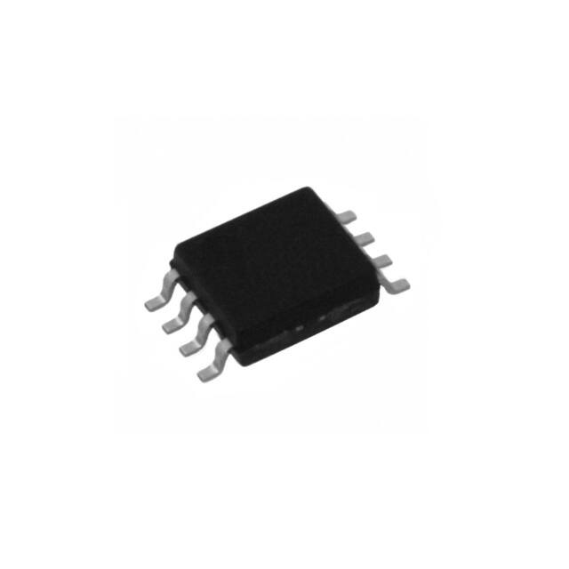
SO-8
Top View
Applications
l
Control MOSFET of Sync-Buck Converters used for Notebook Processor Power
l
Control MOSFET for Isolated DC-DC Converters in Networking Systems
Features
Benefits
Industry-standard pinout SO-8 Package
Compatible with Existing Surface Mount Techniques
RoHS Compliant, Halogen-Free
MSL1, Industrial qualification
Base Part Number
Package Type
IRF8714PbF-1
SO-8
⇒
Multi-Vendor Compatibility
Easier Manufacturing
Environmentally Friendlier
Increased Reliability
Standard Pack
Form
Quantity
Tube/Bulk
95
Tape and Reel
4000
Orderable Part Number
IRF8714PbF-1
IRF8714TRPbF-1
Absolute Maximum Ratings
Max.
Units
VDS
Drain-to-Source Voltage
Parameter
30
V
VGS
Gate-to-Source Voltage
Continuous Drain Current, VGS @ 10V
± 20
ID @ TA = 25°C
14
Continuous Drain Current, VGS @ 10V
Pulsed Drain Current
110
PD @TA = 25°C
Power Dissipation
2.5
PD @TA = 70°C
Power Dissipation
1.6
TJ
Linear Derating Factor
Operating Junction and
TSTG
Storage Temperature Range
ID @ TA = 70°C
IDM
11
c
A
W
W/°C
°C
0.02
-55 to + 150
Thermal Resistance
Parameter
RθJL
RθJA
g
Junction-to-Ambient fg
Junction-to-Drain Lead
Typ.
Max.
Units
–––
20
°C/W
–––
50
Notes through
are on page 9
1
www.irf.com © 2013 International Rectifier
Submit Datasheet Feedback
November 22, 2013
�IRF8714PbF-1
Static @ TJ = 25°C (unless otherwise specified)
Parameter
BVDSS
ΔΒVDSS/ΔTJ
Min. Typ. Max. Units
30
–––
–––
Breakdown Voltage Temp. Coefficient
Static Drain-to-Source On-Resistance
–––
–––
0.021
7.1
–––
8.7
Gate Threshold Voltage
–––
1.35
10.9
1.80
13
2.35
IDSS
Gate Threshold Voltage Coefficient
Drain-to-Source Leakage Current
–––
–––
-6.0
–––
–––
1.0
IGSS
Gate-to-Source Forward Leakage
–––
–––
–––
–––
150
100
nA
VDS = 24V, VGS = 0V, TJ = 125°C
VGS = 20V
Gate-to-Source Reverse Leakage
Forward Transconductance
–––
71
–––
–––
-100
–––
S
VGS = -20V
VDS = 15V, ID = 11A
Total Gate Charge
Pre-Vth Gate-to-Source Charge
–––
–––
8.1
1.9
12
–––
Post-Vth Gate-to-Source Charge
Gate-to-Drain Charge
–––
–––
1.0
3.0
–––
–––
Qgodr
Qsw
Gate Charge Overdrive
Switch Charge (Qgs2 + Qgd)
–––
–––
2.2
4.0
–––
–––
Qoss
Rg
Output Charge
Gate Resistance
–––
–––
4.8
1.6
–––
2.6
td(on)
tr
Turn-On Delay Time
Rise Time
–––
–––
10
9.9
–––
–––
td(off)
tf
Turn-Off Delay Time
Fall Time
–––
–––
11
5.0
–––
–––
Ciss
Coss
Input Capacitance
Output Capacitance
–––
–––
1020
220
–––
–––
Crss
Reverse Transfer Capacitance
–––
110
–––
RDS(on)
VGS(th)
ΔVGS(th)
gfs
Qg
Qgs1
Qgs2
Qgd
V
Conditions
Drain-to-Source Breakdown Voltage
VGS = 0V, ID = 250μA
V/°C Reference to 25°C, ID = 1mA
mΩ VGS = 10V, ID = 14A
V
e
e
VGS = 4.5V, ID = 11A
VDS = VGS, ID = 25μA
mV/°C VDS = VGS, ID = 25μA
μA VDS = 24V, VGS = 0V
VDS = 15V
nC
VGS = 4.5V
ID = 11A
See Figs. 15 & 16
nC
Ω
VDS = 16V, VGS = 0V
VDD = 15V, VGS = 4.5V
ID = 11A
ns
pF
RG = 1.8Ω
See Fig. 18
VGS = 0V
VDS = 15V
ƒ = 1.0MHz
Avalanche Characteristics
EAS
Parameter
Single Pulse Avalanche Energy
IAR
Avalanche Current
c
d
Typ.
–––
Max.
65
Units
mJ
–––
11
A
Diode Characteristics
Parameter
Min. Typ. Max. Units
Conditions
IS
Continuous Source Current
–––
–––
3.1
ISM
(Body Diode)
Pulsed Source Current
–––
–––
110
VSD
(Body Diode)
Diode Forward Voltage
–––
–––
1.0
V
S
p-n junction diode.
TJ = 25°C, IS = 11A, VGS = 0V
trr
Qrr
Reverse Recovery Time
Reverse Recovery Charge
–––
–––
14
15
21
23
ns
nC
TJ = 25°C, IF = 11A, VDD = 15V
di/dt = 300A/μs
ton
Forward Turn-On Time
�c
2
www.irf.com © 2013 International Rectifier
MOSFET symbol
A
showing the
integral reverse
D
G
e
e
Intrinsic turn-on time is negligible (turn-on is dominated by LS+LD)
Submit Datasheet Feedback
November 22, 2013
�IRF8714PbF-1
1000
1000
ID, Drain-to-Source Current (A)
100
10
BOTTOM
TOP
ID, Drain-to-Source Current (A)
TOP
VGS
10V
5.0V
4.5V
3.5V
3.0V
2.7V
2.5V
2.3V
100
1
0.1
0.01
2.3V
10
1
2.3V
≤60μs PULSE WIDTH
0.001
1
10
0.1
100
1000
0.1
V DS, Drain-to-Source Voltage (V)
10
100
1000
Fig 2. Typical Output Characteristics
1000
2.0
RDS(on) , Drain-to-Source On Resistance
(Normalized)
ID, Drain-to-Source Current (A)
1
V DS, Drain-to-Source Voltage (V)
Fig 1. Typical Output Characteristics
100
T J = 150°C
10
T J = 25°C
1
VDS = 15V
≤60μs PULSE WIDTH
0.1
ID = 14A
VGS = 10V
1.5
1.0
0.5
1
2
3
4
5
VGS, Gate-to-Source Voltage (V)
Fig 3. Typical Transfer Characteristics
3
≤60μs PULSE WIDTH
Tj = 150°C
Tj = 25°C
0.1
BOTTOM
VGS
10V
5.0V
4.5V
3.5V
3.0V
2.7V
2.5V
2.3V
www.irf.com © 2013 International Rectifier
6
-60 -40 -20 0
20 40 60 80 100 120 140 160
T J , Junction Temperature (°C)
Fig 4. Normalized On-Resistance
vs. Temperature
Submit Datasheet Feedback
November 22, 2013
�IRF8714PbF-1
10000
5.0
VGS = 0V,
f = 1 MHZ
C iss = C gs + C gd, C ds SHORTED
C rss = C gd
VGS, Gate-to-Source Voltage (V)
ID= 11A
C, Capacitance (pF)
C oss = C ds + C gd
Ciss
1000
Coss
Crss
100
VDS= 24V
VDS= 15V
4.0
3.0
2.0
1.0
10
0.0
1
10
100
0
VDS, Drain-to-Source Voltage (V)
6
8
10
Fig 6. Typical Gate Charge Vs.
Gate-to-Source Voltage
1000
1000
ID, Drain-to-Source Current (A)
ISD, Reverse Drain Current (A)
4
QG, Total Gate Charge (nC)
Fig 5. Typical Capacitance vs.
Drain-to-Source Voltage
100
OPERATION IN THIS AREA
LIMITED BY R DS(on)
100
T J = 150°C
T J = 25°C
10
1
1msec
0.1
100μsec
10
10msec
1
T A = 25°C
Tj = 150°C
Single Pulse
VGS = 0V
0.1
0.4
0.6
0.8
1.0
1.2
VSD, Source-to-Drain Voltage (V)
Fig 7. Typical Source-Drain Diode
Forward Voltage
4
2
www.irf.com © 2013 International Rectifier
1.4
0
1
10
VDS, Drain-to-Source Voltage (V)
Fig 8. Maximum Safe Operating Area
Submit Datasheet Feedback
November 22, 2013
100
�IRF8714PbF-1
2.5
VGS(th) , Gate Threshold Voltage (V)
14
ID, Drain Current (A)
12
10
8
6
4
2
0
2.0
ID = 25μA
1.5
1.0
25
50
75
100
125
150
-75 -50 -25
0
25
50
75 100 125 150
T J , Temperature ( °C )
T A , Ambient Temperature (°C)
Fig 9. Maximum Drain Current vs.
Ambient Temperature
Fig 10. Threshold Voltage vs. Temperature
Thermal Response ( Z thJA ) °C/W
100
D = 0.50
0.20
0.10
0.05
0.02
0.01
10
1
SINGLE PULSE
( THERMAL RESPONSE )
0.1
τJ
0.01
R1
R1
τJ
τ1
R2
R2
R3
R3
Ri (°C/W)
R4
R4
τA
τ1
τ2
τ2
τ3
τ3
τ4
τ4
Ci= τi/Ri
Ci= τi/Ri
0.001
1E-006
1E-005
0.0001
0.001
τA
1.9778
τi (sec)
0.000165
7.4731
0.022044
26.2617
0.82275
14.2991
28.4
0.01
Notes:
1. Duty Factor D = t1/t2
2. Peak Tj = P dm x Zthja + T A
0.1
1
10
t1 , Rectangular Pulse Duration (sec)
Fig 11. Maximum Effective Transient Thermal Impedance, Junction-to-Ambient
5
www.irf.com © 2013 International Rectifier
Submit Datasheet Feedback
November 22, 2013
100
�IRF8714PbF-1
300
EAS , Single Pulse Avalanche Energy (mJ)
RDS(on), Drain-to -Source On Resistance (m Ω)
25
ID = 14A
20
15
TJ = 125°C
10
T J = 25°C
ID
TOP
0.82A
1.0A
BOTTOM 11A
250
200
150
100
50
5
0
3
4
5
6
7
8
9
10
11
12
25
50
75
100
125
150
Starting T J , Junction Temperature (°C)
VGS, Gate -to -Source Voltage (V)
Fig 13. Maximum Avalanche Energy
vs. Drain Current
Fig 12. On-Resistance vs. Gate Voltage
V(BR)DSS
tp
15V
L
VDS
DUT
DRIVER
0
D.U.T
RG
IAS
20V
L
tp
0.01Ω
+
- VDD
1K
20K
VCC
S
A
I AS
Fig 15. Gate Charge Test Circuit
Fig 14. Unclamped Inductive Test Circuit
and Waveform
Id
Vds
Vgs
Vgs(th)
Qgodr
Qgd
Qgs2 Qgs1
Fig 16. Gate Charge Waveform
6
www.irf.com © 2013 International Rectifier
Submit Datasheet Feedback
November 22, 2013
�IRF8714PbF-1
D.U.T
Driver Gate Drive
P.W.
+
+
-
-
*
D.U.T. ISD Waveform
Reverse
Recovery
Current
+
RG
•
•
•
•
dv/dt controlled by RG
Driver same type as D.U.T.
I SD controlled by Duty Factor "D"
D.U.T. - Device Under Test
V DD
P.W.
Period
VGS=10V
Circuit Layout Considerations
• Low Stray Inductance
• Ground Plane
• Low Leakage Inductance
Current Transformer
D=
Period
+
-
Body Diode Forward
Current
di/dt
D.U.T. VDS Waveform
Diode Recovery
dv/dt
Re-Applied
Voltage
Body Diode
VDD
Forward Drop
Inductor Curent
ISD
Ripple ≤ 5%
* VGS = 5V for Logic Level Devices
Fig 17. Peak Diode Recovery dv/dt Test Circuit for N-Channel
HEXFET® Power MOSFETs
V DS
VGS
RG
RD
VDS
90%
D.U.T.
+
-V DD
VGS
Pulse Width ≤ 1 µs
Duty Factor ≤ 0.1 %
Fig 18a. Switching Time Test Circuit
7
www.irf.com © 2013 International Rectifier
10%
VGS
td(on)
tr
td(off) tf
Fig 18b. Switching Time Waveforms
Submit Datasheet Feedback
November 22, 2013
�IRF8714PbF-1
SO-8 Package Outline
Dimensions are shown in milimeters (inches)
D
DIM
B
5
A
6
8
7
6
5
1
2
3
4
H
E
6X
0.25 [.010]
A
e
e1
8X b
0.25 [.010]
A
A1
INCH E S
MIL L IME T E R S
MIN
MAX
MIN
A
.0532
.0688
1.35
1.75
MAX
A1
.0040
.0098
0.10
0.25
b
.013
.020
0.33
0.51
c
.0075
.0098
0.19
0.25
D
.189
.1968
4.80
5.00
E
.1497
.1574
3.80
4.00
e
.050 B AS IC
1.27 B AS IC
e1
.025 B AS IC
0.635 B AS IC
H
.2284
.2440
5.80
6.20
K
.0099
.0196
0.25
0.50
L
.016
.050
0.40
1.27
y
0°
8°
0°
8°
K x 45°
C
y
0.10 [.004]
8X c
8X L
7
C A B
FOOTPRINT
8X 0.72 [.028]
NOTES :
1. DIMENS IONING & T OLERANCING PER AS ME Y14.5M-1994.
2. CONT ROLLING DIMENS ION: MILLIMET ER
3. DIMENS IONS ARE SHOWN IN MILLIMETERS [INCHES ].
4. OUT LINE CONFORMS TO JEDEC OUT LINE MS -012AA.
5 DIMENS ION DOES NOT INCLUDE MOLD PROT RUSIONS .
MOLD PROTRUS IONS NOT T O EXCEED 0.15 [.006].
6.46 [.255]
6 DIMENS ION DOES NOT INCLUDE MOLD PROT RUSIONS .
MOLD PROTRUS IONS NOT T O EXCEED 0.25 [.010].
7 DIMENS ION IS THE LENGT H OF LEAD FOR SOLDERING T O
A S UBS TRAT E.
3X 1.27 [.050]
8X 1.78 [.070]
SO-8 Part Marking Information
E XAMPLE : T HIS IS AN IR F 7101 (MOS F E T )
INT E R NAT IONAL
R E CT IF IE R
LOGO
XXXX
F 7101
DAT E CODE (YWW)
P = DIS GNAT E S LE AD - F R E E
PR ODU CT (OPT IONAL)
Y = L AS T DIGIT OF T H E YE AR
WW = WE E K
A = AS S E MB L Y S IT E CODE
L OT CODE
P AR T NU MB E R
Note: For the most current drawing please refer to IR website at http://www.irf.com/package/
8
www.irf.com © 2013 International Rectifier
Submit Datasheet Feedback
November 22, 2013
�IRF8714PbF-1
SO-8 Tape and Reel (Dimensions are shown in milimeters (inches))
TERMINAL NUMBER 1
12.3 ( .484 )
11.7 ( .461 )
8.1 ( .318 )
7.9 ( .312 )
FEED DIRECTION
NOTES:
1. CONTROLLING DIMENSION : MILLIMETER.
2. ALL DIMENSIONS ARE SHOWN IN MILLIMETERS(INCHES).
3. OUTLINE CONFORMS TO EIA-481 & EIA-541.
330.00
(12.992)
MAX.
14.40 ( .566 )
12.40 ( .488 )
NOTES :
1. CONTROLLING DIMENSION : MILLIMETER.
2. OUTLINE CONFORMS TO EIA-481 & EIA-541.
Note: For the most current drawing please refer to IR website at http://www.irf.com/package/
†
Qualification information
Industrial
Qualification level
Moisture Sensitivity Level
(per JEDE C JE S D47F
SO-8
RoHS compliant
††
guidelines)
MS L1
††
(per JEDE C J-S T D-020D )
Yes
† Qualification standards can be found at International Rectifier’s web site: http://www.irf.com/product-info/reliability
†† Applicable version of JEDEC standard at the time of product release
Notes:
Repetitive rating; pulse width limited by max. junction temperature.
Starting TJ = 25°C, L = 1.1mH, RG = 25Ω, IAS = 11A.
Pulse width ≤ 400μs; duty cycle ≤ 2%.
When mounted on 1 inch square copper board.
Rθ is measured at TJ of approximately 90°C.
IR WORLD HEADQUARTERS: 101 N. Sepulveda Blvd., El Segundo, California 90245, USA
To contact International Rectifier, please visit http://www.irf.com/whoto-call/
9
www.irf.com © 2013 International Rectifier
Submit Datasheet Feedback
November 22, 2013
�


 工商网监
湘ICP备2023018690号
工商网监
湘ICP备2023018690号
