IRFP150MPbF
IR MOSFET™
Features
Advanced Process Technology
Dynamic dv/dt Rating
175°C Operating Temperature
Fast Switching
Fully Avalanche Rated
Lead-Free
V(BR)DSS
100V
RDS(on) max.
0.036
ID
42A
Description
IR MOSFET™ technology from Infineon utilizes
advanced processing techniques to achieve extremely
low on-resistance per silicon area. This benefit,
combined with the fast switching speed and rugged
device design that IR MOSFET™ devices are well
known for, provides the designer with an extremely
efficient and reliable device for use in a wide variety of
applications.
TO-247AD
The TO-247 package is preferred for commercialindustrial applications where higher power levels
preclude the use of TO-220 devices. The TO-247 is
similar but superior to the earlier TO-218 package
because of its isolated mounting hole.
Base part number
Package Type
IRFP150MPbF
TO-247AD
G
Gate
D
Drain
Standard Pack
Form
Quantity
Tube
25
S
Source
Orderable Part Number
IRFP150MPbF
Absolute Maximum Ratings
Symbol
Parameter
ID @ TC = 25°C
Continuous Drain Current, VGS @ 10V
42
ID @ TC = 100°C
IDM
Continuous Drain Current, VGS @ 10V
Pulsed Drain Current
30
140
PD @TC = 25°C
Maximum Power Dissipation
160
W
1.1
± 20
420
22
16
5.0
W/°C
Linear Derating Factor
Gate-to-Source Voltage
Single Pulse Avalanche Energy
Avalanche Current
Repetitive Avalanche Energy
Peak Diode Recovery dv/dt
Operating Junction and
Storage Temperature Range
Soldering Temperature, for 10 seconds (1.6mm from case)
Mounting torque, 6-32 or M3 screw
VGS
EAS
IAR
EAR
dv/dt
TJ
TSTG
Max.
Units
A
V
mJ
A
mJ
V/ns
-55 to + 175
°C
300
10 lbf•in (1.1N•m)
Thermal Resistance
Symbol
RJC
RCS
RJA
1
Parameter
Junction-to-Case
Case-to-Sink, Flat, Greased Surface
Junction-to-Ambient
Typ.
–––
0.24
–––
Max.
0.95
–––
40
Units
°C/W
2020-05-28
�IRFP150MPbF
Electrical characteristics @ TJ = 25°C (unless otherwise specified)
V(BR)DSS
V(BR)DSS/TJ
RDS(on)
VGS(th)
gfs
Parameter
Drain-to-Source Breakdown Voltage
Breakdown Voltage Temp. Coefficient
Static Drain-to-Source On-Resistance
Gate Threshold Voltage
Forward Trans conductance
IDSS
Drain-to-Source Leakage Current
IGSS
Gate-to-Source Forward Leakage
Gate-to-Source Reverse Leakage
Min.
100
–––
–––
2.0
14
–––
–––
–––
–––
Typ. Max. Units
Conditions
––– –––
V VGS = 0V, ID = 250µA
0.11 ––– V/°C Reference to 25°C, ID = 1mA
––– 0.036 VGS = 10V, ID = 23A
–––
4.0
V VDS = VGS, ID = 250µA
––– –––
S VDS = 25V, ID = 22A
–––
25
VDS = 100V, VGS = 0V
µA
––– 250
VDS = 80V,VGS = 0V,TJ =150°C
––– 100
VGS = 20V
nA
––– -100
VGS = -20V
Dynamic Electrical Characteristics @ T J = 25°C (unless otherwise specified)
Qg
Qgs
Qgd
td(on)
tr
td(off)
tf
Total Gate Charge
Gate-to-Source Charge
Gate-to-Drain Charge
Turn-On Delay Time
Rise Time
Turn-Off Delay Time
Fall Time
–––
–––
–––
–––
–––
–––
–––
–––
–––
–––
11
56
45
40
110
15
58
LD
Internal Drain Inductance
–––
5.0
–––
LS
Internal Source Inductance
–––
13
–––
–––
–––
–––
–––
–––
–––
ID = 22A
nC VDS = 80V
VGS = 10V, See Fig.6 and 13
VDD = 50V
ID = 22A
ns
RG= 3.6
RD= 2.3 See Fig.10
Between lead,
6mm (0.25in.)
nH
from package
and center of die contact
VGS = 0V
pF VDS = 25V
ƒ = 1.0MHz, See Fig.5
Ciss
Input Capacitance
Coss
Output Capacitance
Crss
Reverse Transfer Capacitance
Diode Characteristics
Parameter
Continuous Source Current
IS
(Body Diode)
Pulsed Source Current
ISM
(Body Diode)
–––
–––
–––
1900
450
230
Min.
Typ. Max. Units
–––
–––
–––
–––
140
VSD
Diode Forward Voltage
–––
–––
1.3
trr
Qrr
Reverse Recovery Time
Reverse Recovery Charge
–––
–––
180
1.2
270
1.8
42
A
V
Conditions
MOSFET symbol
showing the
integral reverse
p-n junction diode.
TJ = 25°C,IS = 23A,VGS = 0V
ns TJ = 25°C ,IF = 22A
µC di/dt = 100A/µs
Notes:
Repetitive rating; pulse width limited by max. junction temperature. (See fig. 11).
VDD = 25V, TJ = 25°C, L = 1.7mH, RG = 25, IAS = 22A.(See fig. 12).
ISD 22A, di/dt 180A/µs, VDD V(BR)DSS, TJ 175°C.
Pulse width 300µs; duty cycle 2%.
Uses IRF1310N data and test conditions.
2
2020-05-28
�IRFP150MPbF
Fig. 1 Typical Output Characteristics
Fig. 3 Typical Transfer Characteristics
3
Fig. 2 Typical Output Characteristics
Fig. 4 Normalized On-Resistance vs. Temperature
2020-05-28
�IRFP150MPbF
Fig 5. Typical Capacitance vs.
Drain-to-Source Voltage
Fig. 7 Typical Source-to-Drain Diode
Forward Voltage
4
Fig 6. Typical Gate Charge vs.
Gate-to-Source Voltage
Fig 8. Maximum Safe Operating Area
2020-05-28
�IRFP150MPbF
Fig 10a. Switching Time Test Circuit
Fig 9. Maximum Drain Current vs. Case
Temperature
Fig 10a. Switching Time Waveforms
Fig 11. Maximum Effective Transient Thermal Impedance, Junction -to-Case
5
2020-05-28
�IRFP150MPbF
Fig. 12a. Unclamped Inductive Test Circuit
Fig 12c. Maximum Avalanche Energy
vs. Drain Current
Fig. 12b. Unclamped Inductive Waveforms
Fig 13a. Basic Gate Charge Waveform
6
Fig 13b. Gate Charge Test Circuit
2020-05-28
�IRFP150MPbF
Fig 14. Peak Diode Recovery dv/dt Test Circuit for N-Channel
IR MOSFET™
7
2020-05-28
�IRFP150MPbF
TO-247AD Package Outline (Dimensions are shown in millimeters (inches))
PG-TO247-3-21, -41, -44
DIMENSIONS
A
A1
A2
b
b1
b2
c
D
D1
D2
E
E1
E2
E3
e
L
L1
P
Q
S
MILLIMETERS
MIN.
MAX.
4.70
5.30
2.20
2.60
1.50
2.50
1.00
1.40
1.60
2.41
2.57
3.43
0.38
0.89
20.70
21.50
13.08
17.65
0.51
1.35
15.50
16.30
12.38
14.15
3.40
5.10
1.00
2.60
5.44
19.80
20.40
3.85
4.50
3.50
3.70
5.35
6.25
6.04
6.30
DOCUMENT NO.
Z8B00003327
REVISION
06
SCALE 3:1
0 1 2 3 4 5mm
EUROPEAN PROJECTION
ISSUE DATE
25.07.2018
TO-247AD Part Marking Information
8
2020-05-28
�IRFP150MPbF
Revision History
Date
05/28/2020
Comments
Updated datasheet with corporate template
Updated Package picture-page1
Corrected from “Hexfet power MOSFET” to “ IR MOSFET™” -page1 &7
Corrected part marking from TO-247AC to TO-247AD on page 8.
Published by
Infineon Technologies AG
81726 München, Germany
© Infineon Technologies AG 2015
All Rights Reserved.
IMPORTANT NOTICE
The information given in this document shall in no event be regarded as a guarantee of conditions or characteristics
(“Beschaffenheitsgarantie”). With respect to any examples, hints or any typical values stated herein and/or any
information regarding the application of the product, Infineon Technologies hereby disclaims any and all warranties and
liabilities of any kind, including without limitation warranties of non-infringement of intellectual property rights of any third
party.
In addition, any information given in this document is subject to customer’s compliance with its obligations stated in this
document and any applicable legal requirements, norms and standards concerning customer’s products and any use of
the product of Infineon Technologies in customer’s applications.
The data contained in this document is exclusively intended for technically trained staff. It is the responsibility of
customer’s technical departments to evaluate the suitability of the product for the intended application and the
completeness of the product information given in this document with respect to such application.
For further information on the product, technology, delivery terms and conditions and prices please contact your nearest
Infineon Technologies office (www.infineon.com).
WARNINGS
Due to technical requirements products may contain dangerous substances. For information on the types in question
please contact your nearest Infineon Technologies office.
Except as otherwise explicitly approved by Infineon Technologies in a written document signed by authorized
representatives of Infineon Technologies, Infineon Technologies’ products may not be used in any applications where a
failure of the product or any consequences of the use thereof can reasonably be expected to result in personal injury.
9
2020-05-28
�
很抱歉,暂时无法提供与“IRFP150MPBF”相匹配的价格&库存,您可以联系我们找货
免费人工找货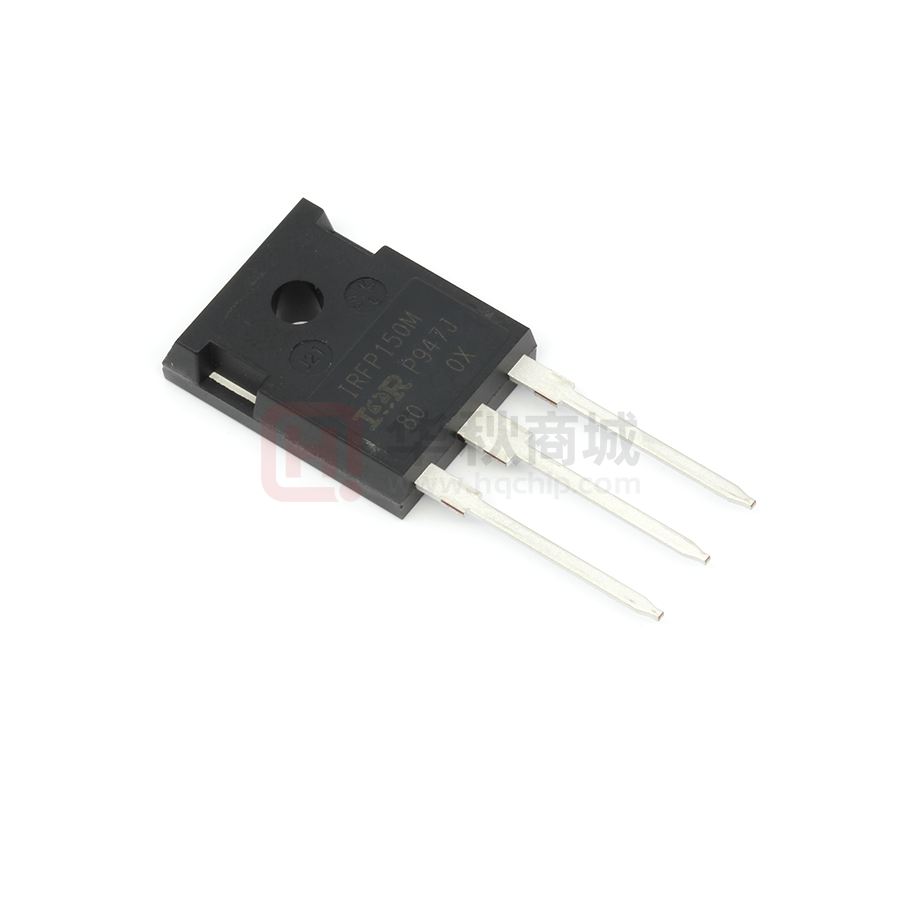


 工商网监
湘ICP备2023018690号
工商网监
湘ICP备2023018690号

