PD - 97175B
IRLR3110ZPbF
IRLU3110ZPbF
Features
l
l
l
l
l
HEXFET® Power MOSFET
Advanced Process Technology
Ultra Low On-Resistance
175°C Operating Temperature
Fast Switching
Repetitive Avalanche Allowed up to Tjmax
D
VDSS = 100V
RDS(on) = 14mΩ
G
Description
Specifically designed for Industrial applications,
this HEXFET® Power MOSFET utilizes the latest
processing techniques to achieve extremely low
on-resistance per silicon area. Additional features
of this design are a 175°C junction operating
temperature, fast switching speed and improved
repetitive avalanche rating . These features combine to make this design an extremely efficient and
reliable device for use in Industrial applications
and a wide variety of other applications.
S
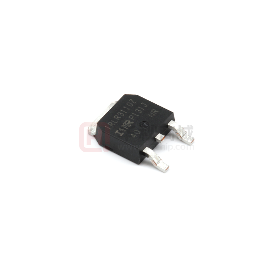
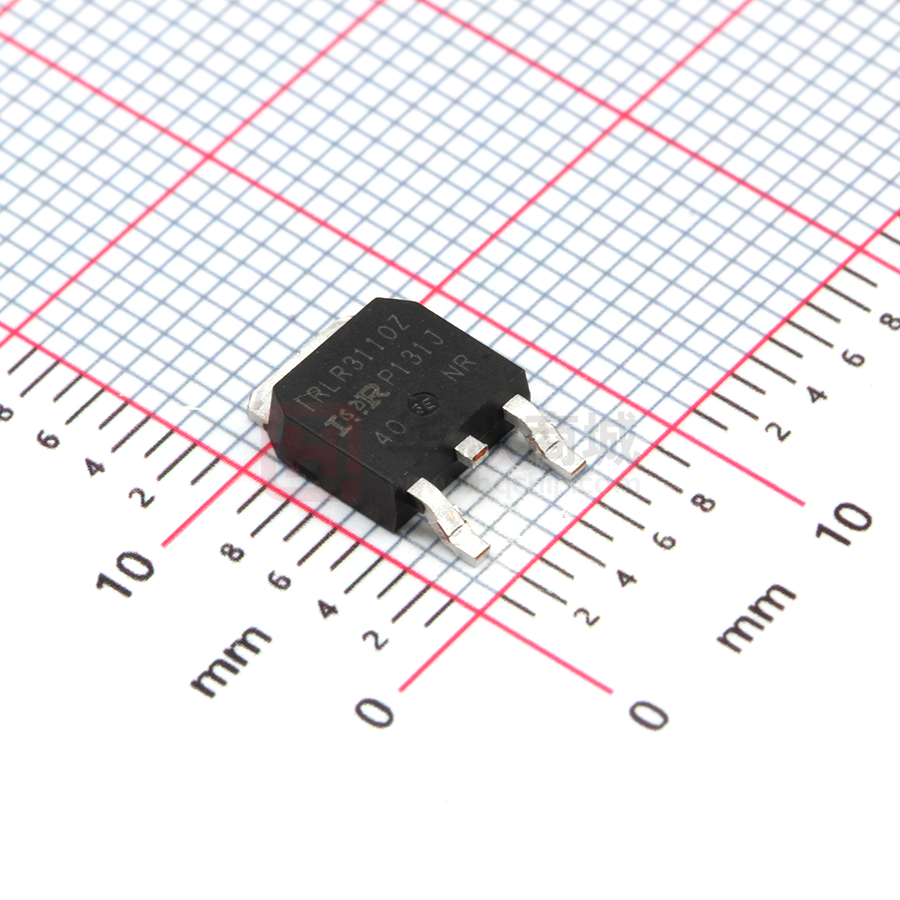
D-Pak
I-Pak
IRLR3110ZPbF IRLU3110ZPbF
Absolute Maximum Ratings
ID @ TC = 25°C
ID @ TC = 100°C
ID @ TC = 25°C
IDM
PD @TC = 25°C
VGS
EAS (Thermally limited)
EAS (Tested )
IAR
EAR
TJ
TSTG
Parameter
Max.
Continuous Drain Current, VGS @ 10V (Silicon Limited)
Continuous Drain Current, VGS @ 10V (Silicon Limited)
Continuous Drain Current, VGS @ 10V (Package Limited)
63
45
42
250
140
c
Pulsed Drain Current
Power Dissipation
Linear Derating Factor
Gate-to-Source Voltage
Single Pulse Avalanche Energy
Single Pulse Avalanche Energy Tested Value
Avalanche Current
Repetitive Avalanche Energy
Operating Junction and
Storage Temperature Range
Reflow Soldering Temperature, for 10 seconds
Mounting Torque, 6-32 or M3 screw
d
�c
h
g
Thermal Resistance
RθJC
RθJA
RθJA
j
Parameter
Junction-to-Case
Junction-to-Ambient (PCB mount)
Junction-to-Ambient
j
ij
Units
A
W
0.95
±16
110
140
See Fig.12a, 12b, 15, 16
W/°C
V
mJ
A
mJ
-55 to + 175
°C
300
10 lbf in (1.1N m)
y
y
Typ.
Max.
Units
–––
–––
–––
1.05
40
110
°C/W
HEXFET® is a registered trademark of International Rectifier.
www.irf.com
1
11/30/09
�IRLR/U3110ZPbF
Electrical Characteristics @ TJ = 25°C (unless otherwise specified)
Parameter
V(BR)DSS
∆V(BR)DSS/∆TJ
RDS(on)
Drain-to-Source Breakdown Voltage
Breakdown Voltage Temp. Coefficient
Static Drain-to-Source On-Resistance
VGS(th)
Gate Threshold Voltage
Forward Transconductance
Drain-to-Source Leakage Current
Min. Typ. Max. Units
Conditions
Qg
Qgs
Qgd
td(on)
tr
td(off)
tf
LD
Gate-to-Source Forward Leakage
Gate-to-Source Reverse Leakage
Total Gate Charge
Gate-to-Source Charge
Gate-to-Drain ("Miller") Charge
Turn-On Delay Time
Rise Time
Turn-Off Delay Time
Fall Time
Internal Drain Inductance
100
–––
–––
–––
1.0
52
–––
–––
–––
–––
–––
–––
–––
–––
–––
–––
–––
–––
–––
0.077
11
12
–––
–––
–––
–––
–––
–––
34
10
15
24
110
33
48
4.5
–––
–––
14
16
2.5
–––
20
250
200
-200
48
–––
–––
–––
–––
–––
–––
–––
LS
Internal Source Inductance
–––
7.5
–––
6mm (0.25in.)
from package
Ciss
Coss
Crss
Coss
Coss
Coss eff.
Input Capacitance
Output Capacitance
Reverse Transfer Capacitance
Output Capacitance
Output Capacitance
Effective Output Capacitance
–––
–––
–––
–––
–––
–––
3980
310
130
1820
170
320
–––
–––
–––
–––
–––
–––
S
and center of die contact
VGS = 0V
VDS = 25V
ƒ = 1.0MHz
VGS = 0V, VDS = 1.0V, ƒ = 1.0MHz
VGS = 0V, VDS = 80V, ƒ = 1.0MHz
VGS = 0V, VDS = 0V to 80V
gfs
IDSS
IGSS
V VGS = 0V, ID = 250µA
V/°C Reference to 25°C, ID = 1mA
mΩ VGS = 10V, ID = 38A
VGS = 4.5V, ID = 32A
V VDS = VGS, ID = 100µA
S VDS = 25V, ID = 38A
µA VDS = 100V, VGS = 0V
VDS = 100V, VGS = 0V, TJ = 125°C
nA VGS = 16V
VGS = -16V
ID = 38A
nC VDS = 50V
VGS = 4.5V
VDD = 50V
ID = 38A
ns RG = 3.7Ω
VGS = 4.5V
D
Between lead,
e
e
e
e
nH
pF
G
f
Source-Drain Ratings and Characteristics
Parameter
Min. Typ. Max. Units
IS
Continuous Source Current
–––
–––
63
ISM
(Body Diode)
Pulsed Source Current
–––
–––
250
VSD
trr
Qrr
ton
(Body Diode)
Diode Forward Voltage
Reverse Recovery Time
Reverse Recovery Charge
Forward Turn-On Time
–––
–––
–––
–––
34
42
1.3
51
63
2
�c
Conditions
MOSFET symbol
A
V
ns
nC
D
showing the
integral reverse
G
S
p-n junction diode.
TJ = 25°C, IS = 38A, VGS = 0V
TJ = 25°C, IF = 38A, VDD = 50V
di/dt = 100A/µs
e
e
Intrinsic turn-on time is negligible (turn-on is dominated by LS+LD)
www.irf.com
�IRLR/U3110ZPbF
1000
1000
TOP
ID, Drain-to-Source Current (A)
100
BOTTOM
10
1
0.1
2.5V
TOP
ID, Drain-to-Source Current (A)
VGS
15V
10V
8.0V
4.5V
3.5V
3.0V
2.7V
2.5V
100
BOTTOM
10
2.5V
≤60µs PULSE WIDTH
≤60µs PULSE WIDTH
Tj = 175°C
Tj = 25°C
0.01
0.1
1
10
1
100
0.1
1000
1
10
100
1000
V DS, Drain-to-Source Voltage (V)
V DS, Drain-to-Source Voltage (V)
Fig 1. Typical Output Characteristics
Fig 2. Typical Output Characteristics
1000
150
Gfs, Forward Transconductance (S)
ID, Drain-to-Source Current (Α)
VGS
15V
10V
8.0V
4.5V
3.5V
3.0V
2.7V
2.5V
T J = 175°C
100
10
T J = 25°C
1
VDS = 25V
≤60µs PULSE WIDTH
0.1
T J = 25°C
125
100
T J = 175°C
75
50
V DS = 10V
300µs PULSE WIDTH
25
0
0
2
4
6
8
10
12
14
VGS, Gate-to-Source Voltage (V)
Fig 3. Typical Transfer Characteristics
www.irf.com
16
0
25
50
75
ID,Drain-to-Source Current (A)
Fig 4. Typical Forward Transconductance
vs. Drain Current
3
�IRLR/U3110ZPbF
100000
VGS, Gate-to-Source Voltage (V)
ID= 38A
C oss = C ds + C gd
10000
C, Capacitance(pF)
5.0
VGS = 0V,
f = 1 MHZ
C iss = C gs + C gd, C ds SHORTED
C rss = C gd
Ciss
1000
Coss
Crss
100
4.0
VDS= 80V
VDS= 50V
3.0
2.0
1.0
10
0.0
1
10
100
0
VDS, Drain-to-Source Voltage (V)
1000
T J = 175°C
ID, Drain-to-Source Current (A)
ISD, Reverse Drain Current (A)
100
20
T J = 25°C
1
100µsec
1msec
10msec
10
DC
Tc = 25°C
Tj = 175°C
Single Pulse
VGS = 0V
0.1
1
0.0 0.2 0.4 0.6 0.8 1.0 1.2 1.4 1.6 1.8
VSD, Source-to-Drain Voltage (V)
Fig 7. Typical Source-Drain Diode
Forward Voltage
4
40
OPERATION IN THIS AREA
LIMITED BY R DS(on)
100
10
30
Fig 6. Typical Gate Charge vs.
Gate-to-Source Voltage
Fig 5. Typical Capacitance vs.
Drain-to-Source Voltage
1000
10
QG Total Gate Charge (nC)
0
1
10
100
1000
VDS, Drain-to-Source Voltage (V)
Fig 8. Maximum Safe Operating Area
www.irf.com
�IRLR/U3110ZPbF
3.0
ID, Drain Current (A)
60
RDS(on) , Drain-to-Source On Resistance
(Normalized)
70
Limited By Package
50
40
30
20
10
0
ID = 63A
VGS = 10V
2.5
2.0
1.5
1.0
0.5
25
50
75
100
125
150
175
-60 -40 -20 0 20 40 60 80 100120140160180
T C , Case Temperature (°C)
T J , Junction Temperature (°C)
Fig 10. Normalized On-Resistance
vs. Temperature
Fig 9. Maximum Drain Current vs.
Case Temperature
Thermal Response ( Z thJC )
10
1
D = 0.50
0.20
0.10
0.05
0.1
τJ
0.02
0.01
0.01
R1
R1
τJ
τ1
R2
R2
τC
τ2
τ1
τ2
τ
Ri (°C/W) τi (sec)
0.383
0.000267
0.667
0.003916
Ci= τi/Ri
Ci i/Ri
Notes:
1. Duty Factor D = t1/t2
2. Peak Tj = P dm x Zthjc + Tc
SINGLE PULSE
( THERMAL RESPONSE )
0.001
1E-006
1E-005
0.0001
0.001
0.01
0.1
t1 , Rectangular Pulse Duration (sec)
Fig 11. Maximum Effective Transient Thermal Impedance, Junction-to-Case
www.irf.com
5
�IRLR/U3110ZPbF
DRIVER
L
VDS
D.U.T
RG
20V
VGS
+
V
- DD
IAS
tp
A
0.01Ω
Fig 12a. Unclamped Inductive Test Circuit
V(BR)DSS
tp
EAS , Single Pulse Avalanche Energy (mJ)
300
15V
ID
4.4A
6.5A
BOTTOM 38A
TOP
250
200
150
100
50
0
25
50
75
100
125
150
175
Starting T J , Junction Temperature (°C)
I AS
Fig 12c. Maximum Avalanche Energy
vs. Drain Current
Fig 12b. Unclamped Inductive Waveforms
QG
QGS
QGD
3.0
VG
Charge
Fig 13a. Basic Gate Charge Waveform
L
DUT
0
1K
VCC
VGS(th) Gate threshold Voltage (V)
10 V
2.5
2.0
1.5
1.0
ID = 100µA
ID = 250µA
ID = 1.0mA
ID = 1.0A
0.5
0.0
-75 -50 -25 0
25 50 75 100 125 150 175 200
T J , Temperature ( °C )
Fig 13b. Gate Charge Test Circuit
6
Fig 14. Threshold Voltage vs. Temperature
www.irf.com
�IRLR/U3110ZPbF
100
Allowed avalanche Current vs avalanche
pulsewidth, tav, assuming ∆ Tj = 150°C and
Tstart =25°C (Single Pulse)
Avalanche Current (A)
Duty Cycle = Single Pulse
0.01
10
0.05
0.10
Allowed avalanche Current vs avalanche
pulsewidth, tav, assuming ∆Τ j = 25°C and
Tstart = 150°C.
1
0.1
1.0E-06
1.0E-05
1.0E-04
1.0E-03
1.0E-02
1.0E-01
tav (sec)
Fig 15. Typical Avalanche Current vs.Pulsewidth
EAR , Avalanche Energy (mJ)
150
TOP
Single Pulse
BOTTOM 1% Duty Cycle
ID = 38A
125
100
75
50
25
0
25
50
75
100
125
150
Starting T J , Junction Temperature (°C)
Fig 16. Maximum Avalanche Energy
vs. Temperature
www.irf.com
175
Notes on Repetitive Avalanche Curves , Figures 15, 16:
(For further info, see AN-1005 at www.irf.com)
1. Avalanche failures assumption:
Purely a thermal phenomenon and failure occurs at a
temperature far in excess of T jmax. This is validated for
every part type.
2. Safe operation in Avalanche is allowed as long as
neither Tjmax nor Iav (max) is exceeded.
3. Equation below based on circuit and waveforms shown in
Figures 12a, 12b.
4. PD (ave) = Average power dissipation per single
avalanche pulse.
5. BV = Rated breakdown voltage (1.3 factor accounts for
voltage increase during avalanche).
6. Iav = Allowable avalanche current.
7. ∆T = Allowable rise in junction temperature, not to exceed
Tjmax (assumed as 25°C in Figure 15, 16).
tav = Average time in avalanche.
D = Duty cycle in avalanche = tav ·f
ZthJC(D, tav ) = Transient thermal resistance, see figure 11)
PD (ave) = 1/2 ( 1.3·BV·Iav) = DT/ ZthJC
Iav = 2DT/ [1.3·BV·Zth]
EAS (AR) = PD (ave)·tav
7
�IRLR/U3110ZPbF
D.U.T
Driver Gate Drive
+
-
•
•
•
•
D.U.T. ISD Waveform
Reverse
Recovery
Current
+
dv/dt controlled by RG
Driver same type as D.U.T.
I SD controlled by Duty Factor "D"
D.U.T. - Device Under Test
P.W.
Period
*
RG
D=
VGS=10V
Circuit Layout Considerations
• Low Stray Inductance
• Ground Plane
• Low Leakage Inductance
Current Transformer
-
Period
P.W.
+
VDD
+
Body Diode Forward
Current
di/dt
D.U.T. VDS Waveform
Diode Recovery
dv/dt
Re-Applied
Voltage
-
Body Diode
VDD
Forward Drop
Inductor Curent
Ripple ≤ 5%
ISD
* VGS = 5V for Logic Level Devices
Fig 17. Peak Diode Recovery dv/dt Test Circuit for N-Channel
HEXFET® Power MOSFETs
V DS
VGS
RG
RD
D.U.T.
+
-VDD
10V
Pulse Width ≤ 1 µs
Duty Factor ≤ 0.1 %
Fig 18a. Switching Time Test Circuit
VDS
90%
10%
VGS
td(on)
tr
t d(off)
tf
Fig 18b. Switching Time Waveforms
8
www.irf.com
�IRLR/U3110ZPbF
D-Pak (TO-252AA) Package Outline
D-Pak (TO-252AA) Part Marking Information
(;$03/(� 7+,6�,6�$1�,5)5���
:,7+�$66(0%/<
/27�&2'(�����
$66(0%/('�21�::���������
,1�7+(�$66(0%/


 工商网监
湘ICP备2023018690号
工商网监
湘ICP备2023018690号
