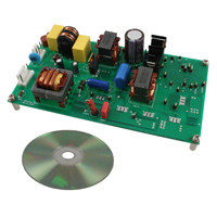
IRPLHID2
HID Ballast for 70W Lamp Using the IRS2573D
Table of Contents
Page
1. Features ........................................................................................... 2
2. Overview .......................................................................................... 3
3. Electrical Characteristic .................................................................... 4
4. Circuit Schematic ............................................................................. 5
5. Functional Description ...................................................................... 7
6. Fault Conditions ............................................................................. 15
7. Dimensioning ................................................................................. 18
8. PCB Layout Considerations ........................................................... 23
9. Bill of Materials ............................................................................... 24
10. IRPLHID2 PCB Layout ................................................................. 26
11. Inductor Specifications ................................................................. 28
www.irf.com
1
-1-
�1. Features
Drives 1 x 70W HID lamp
Input voltage range: 185-265 VAC
High Power Factor / Low Total Harmonic Distortion
Controlled ignition
Low frequency square wave operation
Lamp power and current control
Open circuit and no-lamp protection
Short circuit and lamp failure to warm-up protection
Lamp end-of-life shutdown
IRS2573DSPbF HID Ballast Control IC
www.irf.com
1
-2-
�2. Overview
The IRPLHID2 reference design kit consists of a complete ballast solution for a 70W HID
lamp. The design contains an EMI filter, low voltage power supply, active power factor
correction and a ballast control circuit using the IRS2573D. This demo board is intended
to help with the evaluation of the IRS2573D HID ballast control IC, demonstrate PCB
layout techniques and serve as an aid in the development of production ballasts using
the IRS2573D.
EMI Filter
Rectifier
Active PFC
Buck
Control IC
Low
Voltage
Supply
Buck Control
28
2
27
3
26
4
25
5
6
7
8
9
10
IRS2573D
1
Full-Bridge
Full-Bridge
Control
24
23
Power/Current
Control
22
21
20
Ignition Control
19
11
18
12
17
13
16
14
15
Ignition
Switch
EOL Control
Figure 2.1: IRPLHID2 Block Diagram
www.irf.com
1
-3-
�3. Electrical Characteristic
Parameter
Lamp Power
Input Power
Input Voltage
Input Current
Lamp Running Voltage
Lamp Running Current
Output Frequency
Power Factor
Total Harmonic Distortion
Input AC Voltage Range
Units
[W]
[W]
[VACrms]
[mArms]
[Vpp]
[App]
[Hz]
[%]
[VACrms]
Value
70
73
220
338
160
1.6
149
0.98 at 220 VAC
10 at 220 VAC
185 - 265
TABLE 3.1: Ballast Parameters.
www.irf.com
1
-4-
�4. Circuit Schematic 1
Figure 4.1: IRPLHID2 Circuit Schematic 1
www.irf.com
-5-
�Circuit Schematic 2
Figure 4.2: IRPLHID2 Circuit Schematic 2
www.irf.com
-6-
�5. Functional Description
HID lamps have unique electrical characteristics, and require a careful control method.
Specifically, they require a high voltage for ignition, typically 3 kV to 4 kV, current
limitation during warm-up, and constant power control during running. It is important to
tightly regulate lamp power with respect to lamp voltage to minimize lamp-to-lamp color
and brightness variations. Also, HID lamps should be driven using an AC-voltage to
avoid mercury migration, and at a low frequency, typically less than 200 Hz, to prevent
lamp damage or explosion due to acoustic resonance. All of these requirements are
integrated in the IRS2573D.
Figure 5.1: HID lamp ignition, warm-up and running modes
The IRS2573D is a fully-integrated, fully-protected 600V HID control IC designed to drive
all types of HID lamps. Internal circuitry provides control for ignition, warm-up, running
and fault operating modes. The IRS2573D features include ignition timing control,
constant lamp power control, current limitation control, programmable full-bridge running
frequency, programmable over and under-voltage protection and programmable overcurrent protection. Advanced protection features such as failure of a lamp to ignite,
open load, short-circuit and a programmable fault counter have also been included in the
design.
www.irf.com
1
-7-
�5.1 IRS2573D State and Timing Diagram
Power Turned On
FAULT Mode
Fault Latch Set
Full-Bridge Off (CT=0V)
Buck Off
IGN Timer Off (TIGN=0V)
CLK Off (TCLK=0V)
IQCC 350 A
VCC = 15.6V
All Counters Reset
UVLO Mode
VCC < UVLO(Power Off)
or
RST > VRST+
(Fault Reset)
VCC > UVLO+
and
VSENSE > VOV
and
RST < VRST-
IGN Mode
VSENSE > VOV(2/5) for 787sec
(open circuit)
Good Counter = 2730sec
(No faults detected)
VOV(2/5) < VSENSE < VOV
and
PCOMP > 0.2V
and
ICOMP > 0.5V
IGN (21s 'HIGH'/64s 'LOW')
Ignition Counter Enabled
Buck and Full-Bridge Enabled
CLK and Fault Counters Enabled
Good Counter Reset
VSENSE OVP Enabled
VSENSE > VOV(2/5)
VSENSE < VOV(1/7.5) for 197sec
(short circuit or does not warm up)
or
VSENSE < VOV(1/7.5) for 16384 Events
VCC < UVLO(VCC Fault or Power Down)
Full-Bridge Off (CT=0V)
Buck Off (ICOMP, PCOMP,
TOFF=0V)
IGN Timer Off (TIGN=0V)
CLK Off (TCLK=0V)
IQCC 150 A
Fault and Good Counters Reset
Fault Latch Reset
VSENSE < VOV(2/5)
GENERAL Mode
Full-Bridge Oscillating @ fBRIDGE
Buck Enabled
IGN 'LOW'
CLK and Fault Counters Enabled
VSENSE OVP Enabled
ISENSE Over-current Limitation Enabled
Constant Power Control Enabled
VSENSE > VOV
or
PCOMP < 0.2V
or
ICOMP < 0.2V
VSENSE < VOV(1/7.5)
Reset
Fault and Good
Counters
Reset
Good
Counter
VSENSE < VOV(2/5)
and
PCOMP > 0.2V
and
ICOMP > 0.5V
BUCK OFF Mode
Buck Off
Full-Bridge Oscillating
Fault Counters Enabled
Figure 5.2: IRS2573D state and timing diagram
5.2 Under-voltage Lockout (UVLO) Mode
The under-voltage lockout mode (UVLO) is defined as the state the IC is in when VCC is
below the turn-on threshold of the IC. The IC is designed to maintain an ultra-low supply
current during UVLO mode of 150uA, and to guarantee the IC is fully functional before
www.irf.com
1
-8-
�the buck high-side and full-bridge high and low-side output drivers are activated. The low
voltage power supply is realized with buck converter circuit utilizing the Link Switch
LNK302D (Figure 4.1). Once the voltage on VCC reaches the start-up threshold
(UVLO+), voltage on VSENSE pin is above VOV threshold and the voltage on RST pin is
less than 1.5V, the IC turns on and the full-bridge oscillator (CT) and gate driver outputs
(HO1, LO1, HO2 and LO2) begin to oscillate. During UVLO mode, the full-bridge and
buck are off, the ignition timer and clock are off, the fault and good counters are reset,
and the fault latch is reset.
5.3 Ignition Mode
The ignition timer is enabled when the IC first enters IGN Mode. The ignition timer
frequency is programmed with the external capacitor at the TIGN pin. CTIGN charges up
and down linearly through internal sink and source currents between a fixed voltage
window of 2V and 4V (Figure 5.3). This sets up an internal clock (666ms typical) that is
divided out 128 times and then used to turn the ignition gate driver output (IGN pin) on
and off for a given on and off-time (21sec ‘high’/64sec ‘low’ typical). A logic ‘high’ at the
IGN pin will turn the external ignition MOSFET (MIGN) on and enable the external sidaccontrolled pulse ignition circuit.
666ms
typ.
4V
TIGN
2V
IGN
VLAMP
0V
IGN ENABLED
(21 s typ.)
IGN DISABLED
(64 s typ.)
IGN ENABLED
(21 s typ.)
FAULT
MODE
1180sec typ.
787sec typ.
Figure 5.3: Ignition Timer Timing Diagram
During the ignition phase, the lamp is an open circuit and the buck output voltage is
limited to a maximum value. The ignition circuit comprises of a diac (DIGN), transformer
www.irf.com
1
-9-
�(LIGN), capacitor (CIGN), resistor (RIGN2) and switch (MIGN). When the IC turns on the
switch MIGN, capacitor CIGN discharges through resistor RIGN2. When the voltage
across DIGN reaches the diac threshold voltage (Figure 5.4), DIGN turns on and a
current pulse flows from the buck output, through the primary winding of LIGN and into
capacitor CIGN. This arrangement generates a high-voltage pulse on the secondary to
ignite the lamp. The capacitor CIGN charges up until the diac turns off, and CIGN then
discharges down through resistor RIGN until the diac voltage again reaches the device’s
threshold and another ignition pulse occurs.
V G A T E :M IG N
VCBUCK
V C IG N
V D IA C
t
4KV
VLAM P
t
Figure 5.4: Ignition circuit timing diagram
The ignition circuit will continuously try to ignite the HID lamp for 21sec ‘on’ and 64sec
‘off’ until the lamp ignites. If the lamp does not ignite after 1180sec then the IC will enter
Fault Mode and latch off. If the lamp ignites successfully, the voltage at the VSENSE pin
will fall below VOV(2/5) due to the low impedance of the lamp and the ignition timer will
be disabled (logic ‘low’ at the IGN pin).
5.4 General Mode
During General Mode, the IC reacts to the different load conditions (open-circuit, shortcircuit, lamp warm-up, constant power running, under-voltage lamp faults, transient
under-voltage lamp faults, over-voltage lamp faults, lamp non-strike, etc.) by turning the
buck circuit on or off, adjusting the buck circuit on-time, or counting the occurrence of the
different fault conditions and turning the complete IC off. The IC senses the different
load conditions at the VSENSE and ISENSE pins, compares the voltages at these pins
against the programmed thresholds at the OV and OC pins, and determines the correct
operating mode of the IC (see State Diagram).
5.5 Full-Bridge Control
The IC includes a complete high and low-side full-bridge driver necessary for driving the
www.irf.com
1
- 10 -
�HID lamp with an AC square-wave voltage. The full-bridge begins oscillating at the
programmed frequency immediately when the IC comes out of UVLO Mode and turns
on. The full-bridge is typically driven at a low frequency to prevent acoustic resonances
from damaging the lamp. The full-bridge frequency is programmed with the external
capacitor at the CT pin. CT charges up and down linearly through internal sink and
source currents between a fixed voltage window of 2V and 4V. CT reaching 4V initiates
the toggling of LO1/HO1, and LO2/HO2 respectively (see Figure 5.5). The dead-time is
fixed internally at 1.0us typical. During the dead-time, all full-bridge MOSFETs are off
and the mid-points of each half-bridge are floating or unbiased. Should an external
transient occur during the dead-time due to an ignition voltage pulse, each half-bridge
mid-point (VS1 and VS2 pins) can slew high or low very quickly and exceed the dv/dt
rating of the IC. To prevent this, internal logic guarantees that the IGN pin is set to a
logic ‘low’ during the dead-time. No ignition pulses can occur until the dead-time has
ended and the appropriate full-bridge MOSFETs are turned on. This will guarantee that
the mid-points are biased to the output voltage of the buck or COM before an ignition
pulse occurs. The full-bridge stops oscillating only when the IC enters Fault Mode or
UVLO Mode.
Figure 5.5: Full-bridge timing diagram: CH1 is CT pin voltage, CH2 is LO1 voltage, CH3 is LO2
voltage and CH4 is VS1 pin voltage
5.5 Buck Control
The buck control circuit operates in critical-conduction mode or continuous-conduction
mode depending on the off-time of the buck output or the peak current flowing through
the buck MOSFET (MBUCK). During normal lamp running conditions, the voltage
across the buck current sensing resistor, as measured by the CS pin, is below the
internal over-current threshold (1.2V typical). The buck on-time is defined by the time it
takes for the internal on-time capacitor to charge up to the voltage level on the PCOMP
pin or ICOMP pin, whichever is lower. During the on-time, the current in the buck
www.irf.com
1
- 11 -
�inductor charges up to a peak level, depending on the inductance value, and the
secondary winding output of the buck inductor is at some negative voltage level,
depending on the ratio between the primary and secondary windings. The secondary
winding output is measured by the ZX pin, which clamps the negative voltage to a diode
drop below COM using the internal ESD diode, and limits the resulting negative current
flowing out of the pin with an external resistor, RZX. When the voltage on the internal
on-time capacitor exceeds the voltage on the PCOMP pin or ICOMP pin, the on-time has
ended and the buck output turns off.
The secondary winding output of the buck inductor transitions to some positive voltage
level, depending on the ratio between the primary and secondary windings, and causes
the ZX pin to exceed the internal 2V threshold. The current in the buck inductor begins
to discharge into the lamp full-bridge output stage. When the inductor current reaches
zero, the ZX pin decreases back below the 2V threshold. This causes the internal logic
of the buck control to start the on-time cycle again. This mode of operation is known as
critical-conduction mode because the buck MOSFET is turned on each cycle when the
inductor current discharges to zero. The on-time is programmed by the voltage level on
the PCOMP pin, and the off-time is determined by the time it takes for the inductor
current to discharge to zero, as measured by a negative-going edge on the ZX pin. The
resulting shape of the current in the inductor is triangular with a peak value determined
by the inductance value and on-time setting.
Figure 5.6: Buck control timing diagram (critical conduction mode): CH1 is TOFF pin voltage, CH2 is
ZX pin voltage, CH3 is Buck output voltage and CH4 is current through buck inductor LBUCK
During lamp warm-up or a short-circuit condition at the output, the inductor current will
charge up to an excessive level that can saturate the inductor or damage the buck
MOSFET. To prevent this condition, the buck current sensing resistor (RBCS) is set
such that the voltage at the CS pin exceeds the internal over-current threshold (1.2V
typical) before the inductor saturates. Should the CS pin exceed 1.2V before the internal
www.irf.com
1
- 12 -
�on-time capacitor reaches the voltage level on the PCOMP pin or ICOMP pin, the ontime will end and the buck output will turn off. The off-time is determined by a negativegoing edge on the ZX pin, or, if the maximum off time is reached as programmed by the
time it takes for the CTOFF on the TOFF pin to charge up to an internal threshold of 2V.
If the maximum off-time is reached before the inductor current discharges to zero, then
the inductor will begin charging again from some value above zero. This mode of
operation is known as continuous-conduction mode and results in a continuous DC
current in the inductor with a ripple bounded above by the over-current threshold and
below by the maximum off time setting (see Figure 5.7). Continuous-conduction mode
also allows for a higher average current to flow through the buck inductor before
saturation occurs than with critical-conduction mode.
CS = 1.2V
Figure 5.7: Buck control timing diagram (continuous conduction mode): CH1 is TOFF pin voltage,
CH2 is ZX pin voltage, CH3 is Buck output voltage and CH4 is current through buck inductor LBUCK
5.6 Constant Power Control
During the general mode of operation and after the lamp has ignited, the IC regulates
the lamp output power to a constant level. To achieve this, the IC measures the lamp
voltage and lamp current at the VSENSE and ISENSE pins, multiplies the voltage and
current together using an internal multiplier circuit to calculate power, and regulates the
output of the multiplier circuit to a constant reference voltage by increasing or decreasing
the buck on-time. If the lamp power is too low then the output of the multiplier will be
below the internal reference voltage. The operational trans-conductance amplifier (OTA)
will output a sourcing current to the PCOMP pin that will charge up the CPCOMP to a
higher voltage. This will increase the on-time of buck and increase the output current to
the lamp for increasing the output power. If the lamp power is too high, then the
opposite will occur. The OTA will output a sinking current to the PCOMP pin that will
discharge the CPCOMP to a lower voltage. This will decrease the buck on-time and
www.irf.com
1
- 13 -
�decrease the output current to the lamp for decreasing the output power. The speed of
the constant power control loop is set by the value of the CPCOMP at the PCOMP pin
that determines how fast the loop will react and adjust the buck on-time over the
changing load conditions.
5.7 Current Limitation Control
The constant power control loop will increase or decrease the buck current for
maintaining constant power in the lamp load. During lamp warm-up, the lamp voltage
can be very low (20V typical) and the constant power loop will attempt to increase the
buck current to several amps of current to maintain constant power. This high current
can exceed the manufacturer’s maximum current rating for the HID lamp. To prevent
this condition, an additional current limitation control loop has been included in the IC
Should the voltage at the ISENSE pin exceed the voltage level at the OC pin, another
OTA will sink current from the ICOMP pin. When the ICOMP pin voltage decreases
below the PCOMP pin voltage, then the current limitation loop will override the constant
power loop and the ICOMP pin will decrease the buck on-time. The lower of the
PCOMP or ICOMP pins will override the other and control the buck on-time. When the
lamp eventually warms up and the lamp voltage increases to a level where the lamp
current is below the maximum allowable limit, then the ICOMP pin voltage will increase
above the PCOMP pin voltage, and the PCOMP pin will control the buck on-time again
for maintaining constant power.
5.8 Buck OFF Mode
The IC will enter the Buck-OFF Mode if any one of these 3 conditions occur:
VSENSE > VOV or
PCOMP < 0.2V or
ICOMP < 0.2V
When in the Buck-OFF Mode, the IC will go back to General Mode if all of these 3
conditions are valid:
VSENSE < VOV (2/5)
and
PCOMP > 0.2V
and
ICOMP > 0.5V
The IC will instead go back to Ignition Mode if all of these 3 conditions are valid:
VOV(2/5) < VSENSE < VOV
PCOMP > 0.2V
ICOMP > 0.5V
www.irf.com
and
and
1
- 14 -
�6. Fault Conditions
In case of fault conditions such as open circuit, lamp removal, lamp extinguishes, short
circuit, end-of-life and lamp failure to warm-up, the IRS2573D will go into Fault Mode
after the fault timer times out. In this mode, the internal fault latch is set, full-bridge and
buck are off, ignition and fault timer are off, and the IRS2573D consumes an ultra-low
micro-power current. The IRS2573D can be reset with a fault reset (RST > VRST+) or a
recycling of VCC below and back above the UVLO thresholds. The fault timer is
programmed using the external capacitor CTCLK on the TCLK pin.
6.1 Over-Voltage Fault Counter
The IC includes an over-voltage fault counter at the VSENSE pin. In the IGN Mode, the
over-voltage fault counter will count the time during which an over-voltage condition at
the output of the buck exists due to an open-circuit condition, lamp extinguishes, lamp
removal or end-of-life. Figure 7.1 shows the waveforms when the ballast goes into Fault
Mode because of over-voltage fault. When the voltage at the VSENSE pin remains
above VOV (2/5) and the over-voltage fault counter times out (1180sec typical, with
CTCLK=0.18uF), the IC will enter Fault Mode and shutdown. Before the fault counter
times out, the ignition counter is enabled and the IC keeps trying to ignite the lamp for 21
sec ‘on’ and 64 sec ‘off’.
Figure 6.1: Over-voltage fault: CH1 is the VSENSE voltage, CH2 is IGN pin voltage, CH3 is VCC and
CH4 is LO voltage
www.irf.com
1
- 15 -
�6.2 Under-Voltage Fault Counter
The IC also includes an under-voltage fault counter at the VSENSE pin. Once the lamp
has ignited, the lamp voltage will decrease sharply to a very low voltage (20V typical).
As the lamp warms up, the lamp voltage will slowly increase until the nominal running
voltage is reached (100V typical). If the lamp voltage remains too low for too long, then
this is a lamp fault condition and the ballast must shutdown. To detect this, the VSENSE
pin includes an under-voltage threshold of VOV(1/7.5). If the voltage at the VSENSE pin
remains below VOV(1/7.5) and the under-voltage fault counter times out (295sec typical,
with CTCLK=0.18uF), then the lamp is not warming up properly due to a lamp fault
condition (end of life, etc.) and the IC will enter fault mode and shutdown. If the voltage
at the VSENSE pin increases above VOV(1/7.5) before the under-voltage counter times
out, then the lamp has successfully warmed up and the IC will remain in general mode.
Figure 6.2 shows some waveforms when the ballast goes into Fault Mode due to undervoltage fault.
Figure 6.2: Under-voltage fault: CH1 is TCLK pin voltage, CH2 is VSENSE voltage, CH3 is LO voltage
and CH4 is VCC voltage
6.3 Fast Transient Under-Voltage Fault Counter
During normal running conditions, fast transient under-voltage spikes can occur on the
lamp voltage due to instabilities in the lamp arc. The resulting transients on the
VSENSE pin will cycle below and above the VOV(1/7.5) threshold quickly (= VOV → Buck over voltage threshold (100% of OV)
During the ignition phase the buck voltage is regulated to OV (e.g. 330V). If the buck
voltage stays below 13% of OV for more than 295sec or above 40% of OV for 1180sec,
the ballast will go to Fault mode and latched.
7.3 Dimensioning: Buck settings
Lamp parameter
Start with the lamp parameter:
PLAMP=73W
VLAMP=100V
ILAMP=0.73A
Buck current sensing resistor
Buck inductor over-current protection is setup by buck current sensing resistor:
I OC 0.9 A
I OC ,PEAK 2 I OC 1.8 A
www.irf.com
(7)
- 19 -
�RBCS
VCS
IOC , PEAK
1.2V
0.667
1.8 A
(8)
Buck inductor value
Select input voltage for the buck, which is the bus voltage provided by boost PFC
stage:
VBUS 400V
Select nominal frequency of the buck:
f 70kHz
Calculate buck inductor value based on nominal frequency, lamp current, buck input
and output voltage:
L
T
2 I LAMP
VOUT
1
VBUS
VOUT 733H
(9)
1
and VOUT VLAMP
f
where T
Buck inductor selection value:
L 750H
Buck off-time programming capacitor
Determine buck output minimum voltage (lamp minimum voltage after ignition):
VOUT ,MIN 20V (typical )
Calculate buck minimum frequency in the boundary between critical- and
continuous- conduction mode:
2
VOUT ,MIN
f MIN
VOUT ,MIN
I OC , PEAK L
VBUS
1
20 2
20
14kHz
1.8 750e 6
400
1
www.irf.com
(10)
- 20 -
�Calculate tOFF:
1
VOUT ,MIN
tOFF
VBUS
f
20
400 68s
14
1
(11)
Calculate CTOFF:
CTOFF
I REF t OFF
VTOFF
100A 68s
3.4nF
2V
(12)
Off-time programming capacitor selection value:
CTOFF 3.3nF
Current sense and over-current resistor value:
Calculate the nominal value on VSENSE pin (based on nominal lamp voltage):
VSENSE, NOM VLAMP, NOM
100
RVS 4
RVS 1 RVS 2 RVS 3 RVS 4
7.5k
1.6V
180k 180k 100k 7.5k
(13)
Calculate the nominal value on ISENSE pin:
VISENSE, NOM
www.irf.com
PSENSE
VSENSE, NOM
0.5
0.31V
1.6
(14)
- 21 -
�Calculate the value of current sense and over current resistors:
RCS
ROC
V ISENSE, NOM
I LAMP
0.43
1.5 I OC RCS
11.6k
0.5 I REF
(15)
(16)
Over-current resistor selection value:
ROC 12k
www.irf.com
- 22 -
�8. PCB Layout Considerations
1. Sensitive Timing Components
(inside black box)
2. Filter and Bootstrap Capacitors
3. Signal
Ground
4. Power Ground
1. The programming and timing components should be placed close to the IC with
short traces and with ground connections directly to COM-pin (Pin 6).
2. The filter and bootstrap capacitors should also be placed close to the IC with
short tracks.
3. All signal ground connections should go directly to the COM pin.
4. There is only one connection from the IC COM to the power ground.
The power ground connections should also be as short as possible and with
bigger track size.
Disclaimer
This reference design is intended for evaluation purposes only and has not been
submitted or approved by any external test house for conformance with UL or
international safety or performance standards. International Rectifier does not guarantee
that this reference design will conform to any such standards.
www.irf.com
1
- 23 -
�9. Bill of Materials
Item #
Qty
Manufacturer
Part Number
Description
Reference
1
1
IRS2500S
SO8 PFC IC
IC1
2
1
LNK302DN
Link Switch LNK
IC2
3
4
5
1
1
1
IR
Power
Integration
IR
IR
IR
IRS2573D
IRF840
IRF830
HID Ballast Control IC
MOSFET 500V/600V
MOSFET 500V
6
5
IR
IRGR3B60KD2
IGBT 600V
7
8
9
10
11
1
1
1
1
1
Vishay
Vishay
Vishay
Vishay
Diodes Inc.
8ETH06
LL4148
TZMB15
TZMB36
DF10S
Diode 600V
Diode, 75V, 100mA
Zener Diode, 15V, 500mW, MiniMelf
Zener Diode, 36V, 500mW, MiniMelf
Bridge Rectifier 1A, 1000V
12
5
Diodes Inc.
MURS160
Diode, 600V, 1A, SMB
13
1
K1V26
Sidac 240V-270V
14
1
760801032
Buck Inductor 0.75mH EE20/10/11
LBUCK
15
1
760801070
PFC Inductor 1.5mH EE20/10/11
LPFC
16
1
760370109
Ignition Transformer 1mH EE25/13/7
LIGN
17
18
19
20
21
22
23
24
25
26
1
1
1
2
1
1
1
1
1
1
Schindengen
Würth
Elektronik
Würth
Elektronik
Würth
Elektronik
Panasonic
Epcos
Panasonic
Vishay
Epcos
Roederstein
Wima
Panasonic
Panasonic
Panasonic
IC3
MBUCK
MPFC
MIGN, MH1, ML1,
MH2, ML2
DBUCK
DBUCK1
DVBB2
DVS1
BR1
D3, DVBB1,
DLNK1, DLNK2,
DCS *
DIGN
ELF-15N007A
B82144B1225J000
ECQ-E4105KF
2222 338 20334
B32652A6104J
WY0222MCMBF0K
MKP10 1nF/630V
ECE-A1EN330U
EEU-EB2W220S
ECA-1HM100I
EMI Inductor
HF-Inductor
Capacitor 1µF/400V
Capacitor 330nF/275VAC X2
Capacitor 100nF/630V
Capacitor 2.2nF/275VAC Y Cap
Capacitor 1nF/630V
Capacitor 33µF/25V
Capacitor 22µF/450V
Capacitor 10µF/50V
27
3
Panasonic
ECJ-3YF1E225Z
Capacitor, 2.2uF, 25V, 1206
28
29
30
1
1
1
Panasonic
Panasonic
Multicomp
ECJ-3YB1E105K
ECJ-2FB1E105K
MCCA000282
Capacitor, 1uF, 25V, 1206
Capacitor, 1uF, 25V, 0805
Capacitor, 270nF, 16V, 0805
31
6
Panasonic
ECJ-2YB1H104K
Capacitor, 100nF, 50V, 0805
32
33
1
1
Panasonic
Panasonic
ECJ-2YB1H683K
ECJ-2VB1H333K
Capacitor, 68nF, 50V, 0805
Capacitor, 33nF, 50V, 0805
L1
LLINK1
CBUCK
C1,C2
CIGN
CY
COUT
CLNK3
CBUS
CLNK2
CVB1, CVB2,
CVBB
CTIGN
CPFC2
CTCLK
CVCC1, COV,
COC, CISENSE,
CLINK1, CPFC4
CCT
CPCOMP
34
1
Panasonic
ECJ-2VB1H223K
Capacitor, 22nF, 50V, 0805
CVS
35
1
Panasonic
ECJ-2VB1H472K
Capacitor, 4.7nF, 50V, 0805
CPFC1
36
37
38
39
1
1
1
1
Panasonic
Panasonic
Panasonic
Panasonic
ECJ-2VB1H332K
ECJ-2VB1H102K
ECJ-2VC1H471J
ECJ-2VC1H100D
Capacitor, 3.3nF, 50V, 0805
Capacitor, 1nF, 50V, 0805
Capacitor, 470pF, 50V, 0805
Capacitor, 10pF, 50V, 0805
CTOFF
CICOMP
CCS1
CRZX
* Note: M1 MOSFET has been replaced by DCS on the IRPLHID2 PCB. See the schematic for further details.
www.irf.com
- 24 -
�40
41
42
43
44
2
2
2
1
1
Panasonic
Panasonic
Panasonic
Panasonic
Panasonic
ERJ-8ENF1004V
ERJ-8ENF8203V
ERJ-8ENF1803V
ERJ-6ENF1203V
ERJ-8ENF1003V
Resistor, 1MOhm, 0.25W, 1%, 1206
Resistor, 820kOhm, 0.25W, 1%, 1206
Resistor, 180kOhm, 0.25W, 1%, 1206
Resistor, 120kOhm, 0.125W,1%,0805
Resistor, 100kOhm, 0.25W, 1%, 1206
45
3
Panasonic
ERJ-8ENF6802V
Resistor, 68kOhm, 0.25W, 1%, 1206
46
47
48
49
2
1
1
1
Panasonic
Panasonic
Panasonic
Panasonic
ERJ-6ENF3302V
ERJ-6ENF2002V
ERJ-6ENF1502V
ERJ-6ENF1302V
Resistor, 33kOhm, 0.125W, 1%, 0805
Resistor, 20kOhm, 0.125W, 1%, 0805
Resistor, 15kOhm, 0.125W, 1%, 0805
Resistor, 13kOhm, 0.125W, 1%, 0805
50
3
Panasonic
ERJ-6ENF1002V
Resistor, 10kOhm, 0.125W, 1%, 0805
51
52
53
1
1
1
Panasonic
Panasonic
Panasonic
ERJ-6ENF7501V
ERJ-8ENF3301V
ERJ-6ENF2202V
Resistor, 7.5kOhm, 0.125W, 1%,0805
Resistor, 3.3kOhm, 0.25W, 1%, 1206
Resistor, 2.2kOhm, 0.125W, 1%,0805
54
2
Panasonic
ERJ-6ENF1001V
Resistor, 1kOhm, 0.125W, 1%, 0805
55
8
Panasonic
ERJ-S06F22R0V
Resistor, 22Ohm, 0.125W, 1%, 0805
56
1
Panasonic
ERJ-S06F10R0V
Resistor, 10Ohm, 0.125W, 1%, 0805
57
8
Panasonic
ERJ-8RQF3R3V
Resistor, 3.3Ohm, 0.25W, 1%, 1206
58
3
Panasonic
ERJ-8RQF2R2V
Resistor, 2.2Ohm, 0.25W, 1%, 1206
59
60
61
62
2
1
1
1
ERJ-8RQF1R2V
644753-3
644753-4
Resistor, 1Ohm, 0.25W, 1%, 1206
Resistor 18K/3W
3-pin Connector
4-pin Connector
63
2
FK 237 SA 220 O
Heatsink, TO-220
DBUCK, MBUCK
64
65
1
22
Panasonic
Vishay
Tyco
Tyco
Fisher
Elektronik
-
RPFC1, RPFC2
RPFC4, RPFC5
RVS1, RVS2
ROV
RVS3
RBB2, RBB3,
RBB4
RZX, RPFC8
RIREF
RLNK2
ROC
RPFC3, RPFC6,
RPFC7
RVS4
RLNK3
RLNK1
RISENSE,
RCCS1
RBUCK1, RPFC9,
RIGN1 RHO1,
RLO1, RHO2,
RLO2, RIGN3
RVBB1
RBCS1, RBCS2,
RBCS3, RBCS4,
RBCS5, RCS1,
RCS2, RCS3
RCS4, RCS5,
RCS6
RPFC11, RPFC12
RIGN2
X1
X2
-
Jumper
Test Points
LOUT
-
PR03000201802JAC00
TABLE 9.1: IRPLHID2 Bill of Materials.
www.irf.com
- 25 -
�10. IRPLHID2 PCB Layout
Top Assembly
Top Copper
www.irf.com
1
- 26 -
�Bottom Assembly
Bottom Copper
www.irf.com
1
- 27 -
�11. Inductor specification
Würth Elektronik PN 760801032
www.irf.com
- 28 -
�Würth Elektronik PN 760801070
www.irf.com
- 29 -
�Würth Elektronik PN 760370109
www.irf.com
- 30 -
�


 工商网监
湘ICP备2023018690号
工商网监
湘ICP备2023018690号
