IRS2807DS IRS2817DS
600-V High- and Low-Side Driver with Bootstrap Diode
Features
•
•
•
•
•
•
•
•
•
•
•
•
Product Summary
Floating channel designed for bootstrap operation
Fully operational to +600 V
Tolerant to negative transient voltage, dV/dt immune
Gate drive supply range from 10 V to 20 V
Under-voltage lockout for both channels
3.3 V, 5 V, and 15 V input logic compatible
Matched propagation delay for both channels
Lower di/dt gate driver for better noise immunity
Outputs in phase with inputs
Integrated bootstrap diode
Suitable for both trapezoidal and sinusoidal motor control
RoHS compliant
Description
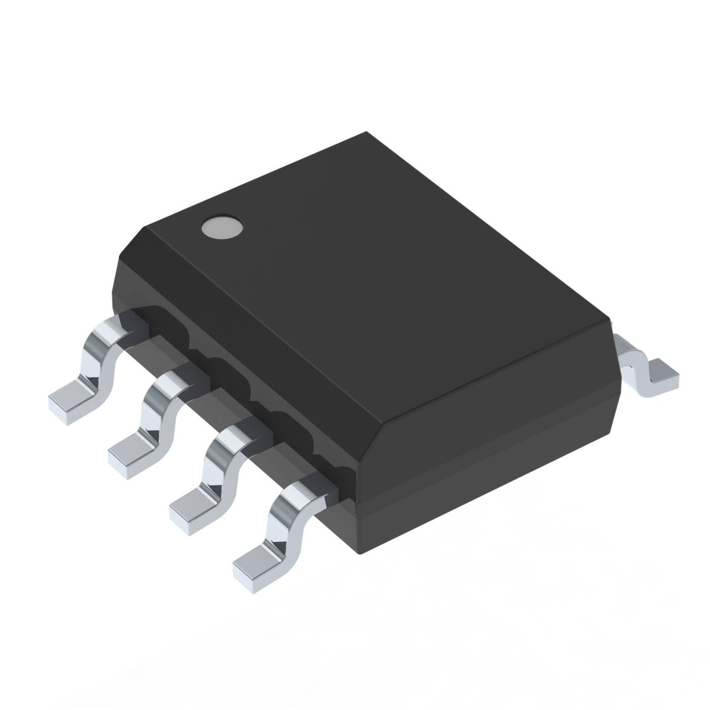
Package Type
IRS2807DS
8-Lead SOIC
IRS2817DS
8-Lead SOIC
Rev 1.1
VOUT
10 V – 20 V
Io+ & I o- (typ.)
200 mA & 350 mA
tON & tOFF (typ.)
515 ns & 500 ns
Delay matching (max.)
50 ns
8-Lead SOIC
Typical Applications
•
•
•
•
•
1
600 V
Package Options
The IRS2817D and IRS2807D are high voltage, high speed
power MOSFET and IGBT drivers with independent high and
low side referenced output channels. Proprietary HVIC and
latch immune CMOS technologies enable ruggedized
monolithic construction. The logic input is compatible with
standard CMOS or LSTTL output, down to 3.3 V logic. The
output drivers feature a high-pulse current buffer stage
designed for minimum driver cross-conduction. The floating
channel can be used to drive N-channel power MOSFETs or
IGBTs in the high side configuration which operates up to 600
V.
Base Part Number
VOFFSET
www.infineon.com
Motor Control
Air Conditioners
Washing Machines
General Purpose Inverters
Micro/Mini Inverter Drives
Standard Pack
Form
Quantity
Tube/Bulk
95
Tape and Reel
2500
Tube/Bulk
95
Tape and Reel
2500
Orderable Part Number
IRS2807DSPBF
IRS2807DSTRPBF
IRS2817DSPBF
IRS2817DSTRPBF
2017-11-27
�IRS2807DS IRS2817DS
Typical Connection Diagram
(Refer to Lead Assignments for correct pin configuration). This diagram shows electrical connections only. Please refer to our
Application Notes & Design Tips for proper circuit board layout.
2
Rev 1.1
www.infineon.com
2017-11-27
�IRS2807DS IRS2817DS
Absolute Maximum Ratings
Absolute Maximum Ratings indicate sustained limits beyond which damage to the device may occur. All voltage parameters
are absolute voltages referenced to COM. The thermal resistance and power dissipation ratings are measured under board
mounted and still air conditions.
Symbol
Definition
Min.
Max.
VB
High side floating supply voltage
-0.3
625
VS
High side floating supply offset voltage
VB - 25
†
VB + 0.3
VHO
High side floating output voltage
VS - 0.3
VB + 0.3
VCC
Low side and logic fixed supply voltage
-0.3
25
VLO
Low side output voltage
-0.3
VCC + 0.3
VIN
Logic input voltage
COM -0.3
VCC + 0.3
Units
V
dVS/dt
Allowable offset supply voltage transient
—
50
V/ns
PD
Package power dissipation @ TA ≤+25ºC
8-Lead SOIC
—
0.625
W
Thermal resistance, junction to ambient
8-Lead SOIC
ºC/W
RthJA
—
200
TJ
Junction temperature
—
150
TS
Storage temperature
-50
150
TL
Lead temperature (soldering, 10 seconds)
—
300
†
ºC
Zener clamps are included between VCC & COM, VB & VS (20 V).
Recommended Operating Conditions
For proper operation the device should be used within the recommended conditions. The VS offset ratings are tested with all
supplies biased at a 15 V differential.
Symbol
Definition
VB
High side floating supply absolute voltage
VS
Static high side floating supply offset voltage
Min
Max
VS +10
VS +20
COM- 8
††
†
600
VSt
Transient high side floating supply offset voltage
VHO
High side floating output voltage
VS
VB
VCC
Low side and logic fixed supply voltage
10
20
VLO
Low side output voltage
VIN
Logic input voltage
TA
Ambient temperature
†
††
-50
Units
600
0
VCC
COM
VCC
-40
125
V
ºC
Logic operational for VS of -8 V to +600 V. Logic state held for VS of -8 V to -VBS
Operational for transient negative VS of COM -50 V with a 50 ns pulse width. Guaranteed by design. Refer to the
Application Information section for more details
3
Rev 1.1
www.infineon.com
2017-11-27
�IRS2807DS IRS2817DS
Static Electrical Characteristics
VCC = VBS = 15 V and TA = 25°C unless otherwise specified. The VIL, VIH, and IIN parameters are referenced to COM and are
applicable to the respective input leads. The VO, IO, and RON parameters are referenced to COM and are applicable to the
respective output leads: HO and LO.
Symbol
Definition
Min.
Typ.
Max.
VIH
Logic “1” input voltage
2.2
—
—
VIL
Logic “0” input voltage
—
—
0.8
VOH
High level output voltage
—
0.8
1.4
VOL
Low level output voltage
—
0.3
0.6
ILK
Offset supply leakage current
—
—
50
IQBS
Quiescent VBS supply current
—
45
70
Quiescent VCC supply current (IRS2807DS)
1000
1700
3000
Quiescent VCC supply current (IRS2817DS)
IQCC
Units
Test Conditions
V
IO = 20 mA
VB = VS = 600 V
µA
VIN = 0 V or 4 V
1000
1800
3000
IIN+
Logic “1” input bias current
—
5
20
VIN = 4 V
IIN-
Logic “0” input bias current
VCC and VBS supply under-voltage positive going
threshold (IRS2807DS)
VCC and VBS supply under-voltage positive going
threshold (IRS2817DS)
VCC and VBS supply under-voltage negative going
threshold (IRS2807DS)
VCC and VBS supply under-voltage negative going
threshold (IRS2817DS)
VCC and VBS supply under-voltage hysteresis
(IRS2807DS)
VCC and VBS supply under-voltage hysteresis
(IRS2817DS)
—
—
2
VIN = 0 V
8.0
8.9
9.8
10.6
11.1
11.6
6.9
7.7
8.5
10.4
10.9
11.4
—
1.2
—
—
0.2
—
VCCUV+
VBSUV+
VCCUVVBSUV-
VCCUVH
VBSUVH
V
IO+
Output high short circuit pulsed current
120
200
—
IO-
Output low short circuit pulsed current
250
350
—
—
200
—
mA
RBS
Bootstrap resistance
†
†
VO = 0 V,
PW ≤ 10 µs
VO = 15 V,
PW ≤ 10 µs
Ω
Please refer to the Application Section for the integrated bootstrap description.
Dynamic Electrical Characteristics
VCC = VB = 15 V, TA = 25ºC, and CL = 1000 pF.
Symbol
Min.
Typ.
ton
Turn-on propagation delay
—
515
715
toff
Turn-off propagation delay
—
500
700
MT
Delay matching, HS & LS turn-on/off
—
—
50
tr
Turn-on rise time
—
150
220
tf
Turn-off fall time
—
50
80
tfil
Minimum pulse input filter time
—
300
—
4
Definition
Rev 1.1
www.infineon.com
Max.
Units
Test Conditions
VS = 0 V or 600 V
ns
VS = 0 V
2017-11-27
�IRS2807DS IRS2817DS
Functional Block Diagram
5
Rev 1.1
www.infineon.com
2017-11-27
�IRS2807DS IRS2817DS
Lead Definitions
Symbol
Description
HIN
Logic input for high side gate driver output (HO), in phase
LIN
Logic input for low side gate driver output (LO), in phase
VB
High side floating supply
HO
High side gate drive output
VS
High side floating supply return
VCC
Low side and logic fixed supply
LO
Low side gate drive output
COM
Low side return
Lead Assignments
8-Lead SOIC
IRS28x7D
6
Rev 1.1
www.infineon.com
2017-11-27
�IRS2807DS IRS2817DS
Application Information and Additional Details
Information regarding the following topics is included as subsections within this section of the datasheet.
•
•
•
•
•
•
•
•
•
•
•
•
IGBT/MOSFET Gate Drive
Switching and Timing Relationships
Matched Propagation Delays
Input Logic Compatibility
Under-voltage Lockout Protection
Advanced Input Filter
Short-Pulse / Noise Rejection
Integrated Bootstrap Functionality
Negative VS Transient SOA
PCB Layout Tips
Integrated Bootstrap FET limitation
Additional Documentation
IGBT/MOSFET Gate Drive
The IRS28x7D HVICs are designed to drive MOSFET or IGBT power devices. Figures 1 and 2 illustrate several parameters
associated with the gate drive functionality of the HVIC. The output current of the HVIC, used to drive the gate of the power
switch, is defined as IO. The voltage that drives the gate of the external power switch is defined as VHO for the high-side power
switch and VLO for the low-side power switch; this parameter is sometimes generically called VOUT and in this case does not
differentiate between the high-side or low-side output voltage.
Figure 1. HVIC sourcing current
7
Rev 1.1
www.infineon.com
Figure 2. HVIC sinking current
2017-11-27
�IRS2807DS IRS2817DS
Switching and Timing Relationships
The relationships between the input and output signals of the IRS28x7D are illustrated below in Figures 3, 4. From these
figures, we can see the definitions of several timing parameters (i.e., PW IN, PW OUT, tON, tOFF, tr, and tf) associated with this
device.
LINx
(or HINx)
50%
50%
PWIN
tON
LOx
(or HOx)
tOFF
tR
tF
PWOUT
90%
10%
90%
10%
Figure 3: Switching time waveforms
Figure 4. Input/output timing diagram
8
Rev 1.1
www.infineon.com
2017-11-27
�IRS2807DS IRS2817DS
Matched Propagation Delays
The IRS28x7D HVICs are designed with propagation delay matching circuitry. With this feature, the IC’s response at the
output to a signal at the input requires approximately the same time duration (i.e., tON, tOFF) for both the low-side channels and
the high-side channels; the maximum difference is specified by the delay matching parameter (MT). The propagation turn-on
delay (tON) of the IRS28x7D is matched to the propagation turn-on delay (tOFF).
Figure 5. Delay Matching Waveform Definition
Input Logic Compatibility
The inputs of this IC are compatible with standard CMOS and TTL outputs. The IRS28x7D have been designed to be
compatible with 3.3 V and 5 V logic-level signals. Figure 8 illustrates an input signal to the IRS28x7D, its input threshold
values, and the logic state of the IC as a result of the input signal.
Figure 6. HIN & LIN input thresholds
9
Rev 1.1
www.infineon.com
2017-11-27
�IRS2807DS IRS2817DS
Under-voltage Lockout Protection
This IC provides under-voltage lockout protection on both the VCC (logic and low-side circuitry) power supply and the VBS (highside circuitry) power supply. Figure 7 is used to illustrate this concept; VCC (or VBS) is plotted over time and as the waveform
crosses the UVLO threshold (VCCUV+/- or VBSUV+/-) the under-voltage protection is enabled or disabled.
Upon power-up, should the VCC voltage fail to reach the VCCUV+ threshold, the IC will not turn-on. Additionally, if the VCC voltage
decreases below the VCCUV- threshold during operation, the under-voltage lockout circuitry will recognize a fault condition and
shutdown the high and low-side gate drive outputs.
Upon power-up, should the VBS voltage fail to reach the VBSUV threshold, the IC will not turn-on. Additionally, if the VBS voltage
decreases below the VBSUV threshold during operation, the under-voltage lockout circuitry will recognize a fault condition, and
shutdown the high-side gate drive outputs of the IC.
The UVLO protection ensures that the IC drives the external power devices only when the gate supply voltage is sufficient to
fully enhance the power devices. Without this feature, the gates of the external power switch could be driven with a low
voltage, resulting in the power switch conducting current while the channel impedance is high; this could result in very high
conduction losses within the power device and could lead to power device failure.
Figure 7. UVLO protection
10
Rev 1.1
www.infineon.com
2017-11-27
�IRS2807DS IRS2817DS
Advanced Input Filter
The advanced input filter allows an improvement in the input/output pulse symmetry of the HVIC and helps to reject noise
spikes and short pulses. This input filter has been applied to the HIN and LIN inputs. The working principle of the new filter is
shown in Figures 8 and 9.
Figure 8 shows a typical input filter and the asymmetry of the input and output. The upper pair of waveforms (Example 1) show
an input signal with a duration much longer then tFIL,IN; the resulting output is approximately the difference between the input
signal and tFIL,IN. The lower pair of waveforms (Example 2) show an input signal with a duration slightly longer then tFIL,IN; the
resulting output is approximately the difference between the input signal and tFIL,IN.
Figure 9 shows the advanced input filter and the symmetry between the input and output. The upper pair of waveforms
(Example 1) show an input signal with a duration much longer then tFIL,IN; the resulting output is approximately the same
duration as the input signal. The lower pair of waveforms (Example 2) show an input signal with a duration slightly longer then
tFIL,IN; the resulting output is approximately the same duration as the input signal.
Figure 8. Typical input filter
Figure 9. Advanced input filter
Short-Pulse / Noise Rejection
Example 2
Example 1
This device’s input filter provides protection against short-pulses (e.g., noise) on the input lines. If the duration of the input
signal is less than tFIL,IN, the output will not change states. Example 1 of Figure 10 shows the input and output in the low state
with positive noise spikes of durations less than tFIL,IN; the output does not change states. Example 2 of Figure 10 shows the
input and output in the high state with negative noise spikes of durations less than tFIL,IN; the output does not change states.
Figure 10. Noise rejecting input filters
Figures 11 and 12 present lab data that illustrates the characteristics of the input filters while receiving ON and OFF pulses.
11
Rev 1.1
www.infineon.com
2017-11-27
�IRS2807DS IRS2817DS
The input filter characteristic is shown in Figure 11; the left side illustrates the narrow pulse ON (short positive pulse)
characteristic while the left shows the narrow pulse OFF (short negative pulse) characteristic. The x-axis of Figure 11 shows
the duration of PWIN, while the y-axis shows the resulting PWOUT duration. It can be seen that for a PWIN duration less than
tFIL,IN, that the resulting PW OUT duration is zero (e.g., the filter rejects the input signal/noise). We also see that once the PWIN
duration exceed tFIL,IN, that the PW OUT durations mimic the PW IN durations very well over this interval with the symmetry
improving as the duration increases. To ensure proper operation of the HVIC, it is suggested that the input pulse width for the
high-side inputs be ≥ 500 ns.
The difference between the PWOUT and PWIN signals of both the narrow ON and narrow OFF cases is shown in Figure 12;
the careful reader will note the scale of the y-axis. The x-axis of Figure 12 shows the duration of PW IN, while the y-axis shows
the resulting PW OUT–PW IN duration. This data illustrates the performance and near symmetry of this input filter.
Narrow Pulse OFF
1000
PWOUT
PWIN
800
600
400
200
0
0
200
400
600
800
1000
Time (ns)
Figure 11. Input filter characteristic
Figure 12. Difference between the input pulse and the output pulse
12
Rev 1.1
www.infineon.com
2017-11-27
�IRS2807DS IRS2817DS
Integrated Bootstrap Functionality
The IRS28x7D embeds an integrated bootstrap FET that allows an alternative drive of the bootstrap supply for a wide range of
applications.
A bootstrap FET is connected between the floating supply VB and VCC (see Fig. 13).
Vcc
BootFet
Vb
Figure 13. Simplified BootFET connection
The bootstrap FET is suitable for most PWM modulation schemes, including trapezoidal control, and can be used either in
parallel with the external bootstrap network (diode+ resistor) or as a replacement of it. The use of the integrated bootstrap as a
replacement of the external bootstrap network may have some limitations at a very high PWM duty cycle due to the bootstrap
FET equivalent resistance (RBS, see page 5).
The integrated bootstrap FET is turned on during the time when LO is ‘high’, and it has a limited source current due to RBS.
The VBS voltage will be charged each cycle depending on the on-time of LO and the value of the CBS capacitor, the drainsource (collector-emitter) drop of the external IGBT (or MOSFET), and the low-side free-wheeling diode drop.
The bootstrap FET follows the state of low-side output stage (i.e., the bootstrap FET is ON when LO is high, unless the VB
voltage is higher than approximately VCC. In that case, the bootstrap FET is designed to remain off until VB returns below that
threshold; this concept is illustrated in Figure 14.
Figure 14. BootFET timing diagram
13
Rev 1.1
www.infineon.com
2017-11-27
�IRS2807DS IRS2817DS
Tolerant to Negative VS Transients
A common problem in today’s high-power switching converters is the transient response of the switch node’s voltage as the
power switches transition on and off quickly while carrying a large current. A typical 3-phase inverter circuit is shown in Figure
15; here we define the power switches and diodes of the inverter.
If the high-side switch (e.g., the IGBT Q1 in Figures 16 and 17) switches off, while the U phase current is flowing to an
inductive load, a current commutation occurs from high-side switch (Q1) to the diode (D2) in parallel with the low-side switch of
the same inverter leg. At the same instance, the voltage node VS1, swings from the positive DC bus voltage to the negative DC
bus voltage.
Figure 15. Three phase inverter
Figure 16. Q1 conducting
Figure 17. D2 conducting
Also when the V phase current flows from the inductive load back to the inverter (see Figures 18 and 19), and Q4 IGBT
switches on, the current commutation occurs from D3 to Q4. At the same instance, the voltage node, VS2, swings from the
positive DC bus voltage to the negative DC bus voltage.
14
Rev 1.1
www.infineon.com
2017-11-27
�IRS2807DS IRS2817DS
Figure 18. D3 conducting
Figure 19. Q4 conducting
However, in a real inverter circuit, the VS voltage swing does not stop at the level of the negative DC bus, rather it swings
below the level of the negative DC bus. This undershoot voltage is called “negative VS transient”.
The circuit shown in Figure 20 depicts one leg of the three phase inverter; Figures 21 and 22 show a simplified illustration of
the commutation of the current between Q1 and D2. The parasitic inductances in the power circuit from the die bonding to the
PCB tracks are lumped together in LC and LE for each IGBT. When the high-side switch is on, VS1 is below the DC+ voltage by
the voltage drops associated with the power switch and the parasitic elements of the circuit. When the high-side power switch
turns off, the load current momentarily flows in the low-side freewheeling diode due to the inductive load connected to VS1 (the
load is not shown in these figures). This current flows from the DC- bus (which is connected to the COM pin of the HVIC) to
the load and a negative voltage between VS1 and the DC- Bus is induced (i.e., the COM pin of the HVIC is at a higher potential
than the VS pin).
Figure 20. Parasitic Elements
Figure 21. VS positive
Figure 22. VS negative
In a typical motor drive system, dV/dt is typically designed to be in the range of 3-5 V/ns. The negative VS transient voltage can
exceed this range during some events such as short circuit and over-current shutdown, when di/dt is greater than in normal
operation.
International Rectifier’s HVICs have been designed for the robustness required in many of today’s demanding applications. An
indication of the IRS28x7D’s robustness can be seen in Figure 23, where there is represented the IRS28x7D Safe Operating
Area at VBS=15 V based on repetitive negative VS spikes. A negative VS transient voltage falling in the grey area (outside SOA)
may lead to IC permanent damage; vice versa unwanted functional anomalies or permanent damage to the IC do not appear if
negative Vs transients fall inside SOA.
15
Rev 1.1
www.infineon.com
2017-11-27
�IRS2807DS IRS2817DS
Figure 23. Negative VS transient SOA for IRS28x7D @ VBS=15 V
Even though the IRS28x7D has been shown able to handle these large negative VS transient conditions, it is highly
recommended that the circuit designer always limit the negative VS transients as much as possible by careful PCB layout and
component use.
PCB Layout Tips
Distance between high and low voltage components: It’s strongly recommended to place the components tied to the floating
voltage pins (VB and VS) near the respective high voltage portions of the device. Please see the Case Outline information in
this datasheet for the details.
Ground Plane: In order to minimize noise coupling, the ground plane should not be placed under or near the high voltage
floating side.
Gate Drive Loops: Current loops behave like antennas and are able to receive and transmit EM noise (see Figure 24). In order
to reduce the EM coupling and improve the power switch turn on/off performance, the gate drive loops must be reduced as
much as possible. Moreover, current can be injected inside the gate drive loop via the IGBT collector-to-gate parasitic
capacitance. The parasitic auto-inductance of the gate loop contributes to developing a voltage across the gate-emitter, thus
increasing the possibility of a self turn-on effect.
16
Rev 1.1
www.infineon.com
2017-11-27
�IRS2807DS IRS2817DS
VBX
(or VCC)
HOX
(or LOX)
IGC
CGC
RG
Gate Drive
Loop
VGE
VSX
(or COM)
Figure 24. Antenna Loops
Supply Capacitor: It is recommended to place a bypass capacitor (CIN) between the VCC and COM pins. A ceramic 1μF
ceramic capacitor is suitable for most applications. This component should be placed as close as possible to the pins in order
to reduce parasitic elements.
Routing and Placement: Power stage PCB parasitic elements can contribute to large negative voltage transients at the switch
node; it is recommended to limit the phase voltage negative transients. In order to avoid such conditions, it is recommended to
1) minimize the high-side emitter to low-side collector distance, and 2) minimize the low-side emitter to negative bus rail stray
inductance. However, where negative VS spikes remain excessive, further steps may be taken to reduce the spike. This
includes placing a resistor (5 Ω or less) between the VS pin and the switch node (see Figure 25), and in some cases using a
clamping diode between COM and VS (see Figure 26). See DT04-4 at www.infineon.com for more detailed information.
Figure 25. VS resistor
Figure 26. VS clamping diode
Additional Documentation
Several technical documents related to the use of HVICs are available at www.infineon.com; use the Site Search function and
the document number to quickly locate them. Below is a short list of some of these documents.
DT97-3: Managing Transients in Control IC Driven Power Stages
AN-1123: Bootstrap Network Analysis: Focusing on the Integrated Bootstrap Functionality
DT04-4: Using Monolithic High Voltage Gate Drivers
AN-978: HV Floating MOS-Gate Driver ICs
17
Rev 1.1
www.infineon.com
2017-11-27
�IRS2807DS IRS2817DS
Parameters trend in temperature
1500
Turn-off Propagation Delay (ns)
Turn-on Propagation Delay (ns)
Figures 27-48 provide information on the experimental performance of the IRS28x7D HVIC. The line plotted in each figure is
generated from actual lab data. A large number of individual samples from multiple wafer lots were tested at three
temperatures (-40ºC, 25ºC, and 125ºC) in order to generate the experimental (Exp.) curve. The line labeled Exp. consist of
three data points (one data point at each of the tested temperatures) that have been connected together to illustrate the
understood trend. The individual data points on the curve were determined by calculating the averaged experimental value of
the parameter (for a given temperature).
1200
900
Exp.
600
300
0
-50
-25
0
25
50
75
100
1000
800
600
Exp.
400
200
0
-50
125
-25
0
Temperature ( C)
Figure 27. Turn-on Propagation Delay vs. Temperature
50
75
100
125
250
Figure 28. Turn-off Propagation Delay vs. Temperature
Turn-Off fall Time (ns)
Turn-On Rise Time (ns)
25
Temperature (oC)
o
200
150
100
Exp.
125
100
75
50
Exp.
25
50
0
0
-50
-25
0
25
50
75
100
o
Temperature ( C)
Figure 29. Turn-on Rise Time vs. Temperature
18
Rev 1.1
www.infineon.com
125
-50
-25
0
25
50
75
100
125
o
Temperature ( C)
Figure 30. Turn-off Rise Time vs. Temperature
2017-11-27
�Output High SC pulsed current (A)
3
2
1
Exp.
0
-50
-25
0
25
50
75
100
125
Output low short circuit pulsed current (A)
IRS2807DS IRS2817DS
3
2
1
Exp.
0
-50
-25
0
25
Temperature (oC)
125
Figure 32. Output Low Short Circuit Pulsed Current vs.
Temperature
4
900
Exp.
600
300
0
-50
-25
0
25
50
75
100
125
VCC supply UV hysteresis ( V)
1200
Tbson_TYP (ns)
100
Temperature ( C)
1500
3
2
Exp.
1
0
-50
-25
0
o
2
Exp.
0
25
50
75
100
125
VCC Quiescent Supply Current (mA)
3
0
75
100
125
Figure 34. VCC Supply UV Hysteresis vs. Temperature
4
-25
50
Temperature ( C)
Figure 33. Tbson_TYP vs. Temperature
-50
25
o
Temperature ( C)
VBS supply UV hysteresis (V)
75
o
Figure 31. Output High SC Pulsed Current vs. Temperature
1
50
10
8
6
4
2
Exp.
0
-50
-25
0
25
50
75
100
125
Temperature ( C)
Temperature (oC)
Figure 35. VBS Supply UV Hysteresis vs. Temperature
Figure 36. VCC Quiescent Supply Current vs. Temperature
o
19
Rev 1.1
www.infineon.com
2017-11-27
�12
100
80
VCCUV+ Threshold (V)
VBS Quiescent Supply Current (uA)
IRS2807DS IRS2817DS
60
Exp.
40
20
9
Exp.
6
3
0
0
-50
-25
0
25
50
75
100
-50
125
-25
0
25
100
125
Temperature ( C)
Figure 37. VBS Quiescent Supply Current vs.
Temperature
Figure 38. VCCUV+ Threshold vs. Temperature
12
12
9
9
VBSUV+ Threshold (V)
VCCUV- Threshold (V)
75
o
Temperature (oC)
Exp.
6
3
Exp.
6
3
0
0
-50
-25
0
25
50
75
100
-50
125
-25
0
25
50
75
100
125
o
Temperature ( C)
Temperature (oC)
Figure 39. VCCUV- Threshold vs. Temperature
Figure 40. VBSUV+ Threshold vs. Temperature
1500
300
200
EXP.
100
0
-50
-25
0
25
50
75
100
125
o
Temperature ( C)
Figure 41. Low Level Output Voltage vs. Temperature
20
Rev 1.1
www.infineon.com
High level output voltage (mV).
400
Low level output voltage (mV)
50
1200
900
Exp.
600
300
0
-50
-25
0
25
50
75
100
125
Temperature (oC)
Figure 42. High Level Output Voltage vs. Temperature
2017-11-27
�12
500
400
V BSUV- Threshold (V)
Bootstrap resistance VCC type (Ohm)
IRS2807DS IRS2817DS
300
200
Exp.
100
9
Exp.
6
3
0
0
-50
-25
0
25
50
75
100
-50
125
-25
0
50
75
100
125
Temperature ( C)
Temperature ( C)
Figure 43. Bootstrap Resistance VCC type vs. Temperature
Figure 44. VBSUV- Threshold vs. Temperature
8
8
6
6
Lin_VTH- (V)
Lin_VTH+ (V)
25
o
o
4
Exp.
2
4
2
Exp.
0
0
-50
-25
0
25
50
75
100
125
-50
-25
0
Tem perature (oC)
75
100
125
Temperature ( C)
Figure 46. Lin_VTH- vs. Temperature
8
8
6
6
Hin_VTH- (V)
Hin_VTH+ (V)
50
o
Figure 45. Lin_VTH+ vs. Temperature
4
Exp.
2
25
4
2
Exp.
0
0
-50
-25
0
25
50
75
100
Temperature (oC)
Figure 47. Hin_VTH+ vs. Temperature
21
Rev 1.1
www.infineon.com
125
-50
-25
0
25
50
75
100
125
Temperature (oC)
Figure 48. Hin_VTH- vs. Temperature
2017-11-27
�IRS2807DS IRS2817DS
Package Details: 8-Lead SOIC
22
Rev 1.1
www.infineon.com
2017-11-27
�IRS2807DS IRS2817DS
Tape and Reel Details: 8-Lead SOIC
LOADED TAPE FEED DIRECTION
A
B
H
D
F
C
NOTE : CONTROLLING
DIMENSION IN MM
E
G
CARRIER TAPE DIMENSION FOR 8SOICN
Metric
Imperial
Code
Min
Max
Min
Max
A
7.90
8.10
0.311
0.318
B
3.90
4.10
0.153
0.161
C
11.70
12.30
0.46
0.484
D
5.45
5.55
0.214
0.218
E
6.30
6.50
0.248
0.255
F
5.10
5.30
0.200
0.208
G
1.50
n/a
0.059
n/a
H
1.50
1.60
0.059
0.062
F
D
C
B
A
E
G
H
REEL DIMENSIONS FOR 8SOICN
Metric
Code
Min
Max
A
329.60
330.25
B
20.95
21.45
C
12.80
13.20
D
1.95
2.45
E
98.00
102.00
F
n/a
18.40
G
14.50
17.10
H
12.40
14.40
23
Rev 1.1
www.infineon.com
Imperial
Min
Max
12.976
13.001
0.824
0.844
0.503
0.519
0.767
0.096
3.858
4.015
n/a
0.724
0.570
0.673
0.488
0.566
2017-11-27
�IRS2807DS IRS2817DS
Part Marking Information
Part number
S2817D
Date code
YWW ?
Pin 1
Identifier
IR logo
? XXXX
?
MARKING CODE
P
Lead Free Released
Lot Code
(Prod mode –
4 digit SPN code)
Assembly site code
Per SCOP 200-002
Non-Lead Free Released
8-Lead SOIC8
IRS2817DSPBF
24
Rev 1.1
www.infineon.com
2017-11-27
�IRS2807DS IRS2817DS
Qualification Information
†
Qualification Level
Moisture Sensitivity Level
Human Body Model
ESD
Machine Model
IC Latch-Up Test
RoHS Compliant
†
Industrial
Comments: This family of ICs has passed JEDEC’s Industrial
qualification. IR’s Consumer qualification level is granted by
extension of the higher Industrial level.
††
MSL2 , 260°C
8-Lead SOIC
(per IPC/JEDEC J-STD-020)
Class 1C
(per JEDEC standard JESD22-A114)
Class B
(per EIA/JEDEC standard EIA/JESD22-A115)
Class I, Level A
(per JESD78)
Yes
Higher qualification ratings may be available should the user have such requirements. Please contact your Infineon
sales representative for further information.
Higher MSL ratings may be available for the specific package types listed here. Please contact your Infineon sales
representative for further information.
††
25
Rev 1.1
www.infineon.com
2017-11-27
�IRS2807DS IRS2817DS
Published by
Infineon Technologies AG
81726 München, Germany
© Infineon Technologies AG 2017
All Rights Reserved.
IMPORTANT NOTICE
The information given in this document shall in no event be regarded as a guarantee of conditions or
characteristics (“Beschaffenheitsgarantie”). With respect to any examples, hints or any typical values stated
herein and/or any information regarding the application of the product, Infineon Technologies hereby disclaims
any and all warranties and liabilities of any kind, including without limitation warranties of non-infringement of
intellectual property rights of any third party.
In addition, any information given in this document is subject to customer’s compliance with its obligations stated
in this document and any applicable legal requirements, norms and standards concerning customer’s products
and any use of the product of Infineon Technologies in customer’s applications.
The data contained in this document is exclusively intended for technically trained staff. It is the responsibility of
customer’s technical departments to evaluate the suitability of the product for the intended application and the
completeness of the product information given in this document with respect to such application.
For further information on the product, technology, delivery terms and conditions and prices please contact your
nearest Infineon Technologies office (www.infineon.com).
WARNINGS
Due to technical requirements products may contain dangerous substances. For information on the types in
question please contact your nearest Infineon Technologies office.
Except as otherwise explicitly approved by Infineon Technologies in a written document signed by authorized
representatives of Infineon Technologies, Infineon Technologies’ products may not be used in any applications
where a failure of the product or any consequences of the use thereof can reasonably be expected to result in
personal injury.
26
Rev 1.1
www.infineon.com
2017-11-27
�


 工商网监
湘ICP备2023018690号
工商网监
湘ICP备2023018690号

