OPTIREG™ linear TLE42754
Low dropout li near voltage regulator
Features
•
Output voltage 5 V ± 2%
•
Ouput current up to 450 mA
•
Very low current consumption
•
Power-on and undervoltage reset with programmable delay time
•
Reset low down to VQ = 1 V
•
Very low dropout voltage
•
Output current limitation
•
Reverse polarity protection
•
Overtemperature protection
•
Suitable for use in automotive electronics
•
Wide temperature range from -40°C up to 150°C
•
Input voltage range from -42 V to 45 V
•
Green Product (RoHS compliant)
Potential applications
General automotive applications.
Product validation
Qualified for automotive applications. Product validation according to AEC-Q100.
Description
The OPTIREG™ linear TLE42754 is a monolithic integrated low-dropout voltage regulator in a 5-pin TOpackage, especially designed for automotive applications. An input voltage up to 42 V is regulated to an
output voltage of 5.0 V. The component is able to drive loads up to 450 mA. It is short-circuit proof by the
implemented current limitation and has an integrated overtemperature shutdown. A reset signal is generated
for an output voltage VQ,rt of typically 4.65 V. The power-on reset delay time can be programmed by the
external delay capacitor.
Datasheet
www.infineon.com/OPTIREG-linear
1
Rev. 1.3
2021-11-25
�OPTIREG™ linear TLE42754
Low dropout linear voltage regulator
Type
Package
Marking
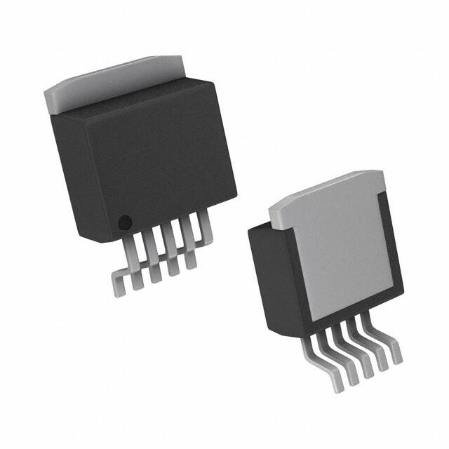
TLE42754D
PG-TO252-5
42754D
TLE42754G
PG-TO263-5
TLE42754
TLE42754E
PG-SSOP-14 exposed pad
42754E
Dimensioning information on external components
An input capacitor CI is recommended for compensation of line influences. An output capacitor CQ is necessary
for the stability of the control loop.
Circuit description
The control amplifier compares a reference voltage to a voltage that is proportional to the output voltage and
drives the base of the series transistor via a buffer. Saturation control as a function of the load current prevents
any oversaturation of the power element. The component also has a number of internal circuits for protection
against:
•
Overload
•
Overtemperature
•
Reverse polarity
Datasheet
2
Rev. 1.3
2021-11-25
�OPTIREG™ linear TLE42754
Low dropout linear voltage regulator
Table of contents
Features . . . . . . . . . . . . . . . . . . . . . . . . . . . . . . . . . . . . . . . . . . . . . . . . . . . . . . . . . . . . . . . . . . . . . . . . 1
Potential applications . . . . . . . . . . . . . . . . . . . . . . . . . . . . . . . . . . . . . . . . . . . . . . . . . . . . . . . . . . . . . 1
Product validation . . . . . . . . . . . . . . . . . . . . . . . . . . . . . . . . . . . . . . . . . . . . . . . . . . . . . . . . . . . . . . . . 1
Description . . . . . . . . . . . . . . . . . . . . . . . . . . . . . . . . . . . . . . . . . . . . . . . . . . . . . . . . . . . . . . . . . . . . . . 1
Table of contents . . . . . . . . . . . . . . . . . . . . . . . . . . . . . . . . . . . . . . . . . . . . . . . . . . . . . . . . . . . . . . . . . 3
1
Block diagram . . . . . . . . . . . . . . . . . . . . . . . . . . . . . . . . . . . . . . . . . . . . . . . . . . . . . . . . . . . . . . . . . . . 4
2
2.1
2.2
2.3
2.4
Pin configuration . . . . . . . . . . . . . . . . . . . . . . . . . . . . . . . . . . . . . . . . . . . . . . . . . . . . . . . . . . . . . . . . .
Pin assignment TLE42754D (PG-TO252-5) and TLE42754G (PG-TO263-5) . . . . . . . . . . . . . . . . . . . . . . .
Pin definitions and functions TLE42754D (PG-TO252-5) and TLE42754G (PG-TO263-5) . . . . . . . . . . .
Pin assignment TLE42754E (PG-SSOP-14 exposed pad) . . . . . . . . . . . . . . . . . . . . . . . . . . . . . . . . . . . . . . .
Pin definitions and functions TLE42754E (PG-SSOP-14 exposed pad) . . . . . . . . . . . . . . . . . . . . . . . . . .
5
5
5
6
6
3
3.1
3.2
3.3
General product characteristics . . . . . . . . . . . . . . . . . . . . . . . . . . . . . . . . . . . . . . . . . . . . . . . . . . . .
Absolute maximum ratings . . . . . . . . . . . . . . . . . . . . . . . . . . . . . . . . . . . . . . . . . . . . . . . . . . . . . . . . . . . . . . . .
Functional range . . . . . . . . . . . . . . . . . . . . . . . . . . . . . . . . . . . . . . . . . . . . . . . . . . . . . . . . . . . . . . . . . . . . . . . . .
Thermal resistance . . . . . . . . . . . . . . . . . . . . . . . . . . . . . . . . . . . . . . . . . . . . . . . . . . . . . . . . . . . . . . . . . . . . . . .
7
7
8
9
4
4.1
4.2
4.3
Block description and electrical characteristics . . . . . . . . . . . . . . . . . . . . . . . . . . . . . . . . . . . . . .
Voltage regulator . . . . . . . . . . . . . . . . . . . . . . . . . . . . . . . . . . . . . . . . . . . . . . . . . . . . . . . . . . . . . . . . . . . . . . . .
Current consumption . . . . . . . . . . . . . . . . . . . . . . . . . . . . . . . . . . . . . . . . . . . . . . . . . . . . . . . . . . . . . . . . . . . .
Reset function . . . . . . . . . . . . . . . . . . . . . . . . . . . . . . . . . . . . . . . . . . . . . . . . . . . . . . . . . . . . . . . . . . . . . . . . . . .
10
10
14
16
5
5.1
5.2
5.2.1
5.2.2
5.3
5.4
Application information . . . . . . . . . . . . . . . . . . . . . . . . . . . . . . . . . . . . . . . . . . . . . . . . . . . . . . . . . .
Application diagram . . . . . . . . . . . . . . . . . . . . . . . . . . . . . . . . . . . . . . . . . . . . . . . . . . . . . . . . . . . . . . . . . . . . .
Selection of external components . . . . . . . . . . . . . . . . . . . . . . . . . . . . . . . . . . . . . . . . . . . . . . . . . . . . . . . . .
Input pin . . . . . . . . . . . . . . . . . . . . . . . . . . . . . . . . . . . . . . . . . . . . . . . . . . . . . . . . . . . . . . . . . . . . . . . . . . . . . .
Output pin . . . . . . . . . . . . . . . . . . . . . . . . . . . . . . . . . . . . . . . . . . . . . . . . . . . . . . . . . . . . . . . . . . . . . . . . . . . .
Thermal considerations . . . . . . . . . . . . . . . . . . . . . . . . . . . . . . . . . . . . . . . . . . . . . . . . . . . . . . . . . . . . . . . . . .
Reverse polarity protection . . . . . . . . . . . . . . . . . . . . . . . . . . . . . . . . . . . . . . . . . . . . . . . . . . . . . . . . . . . . . . .
22
22
22
22
22
23
24
6
Package outlines . . . . . . . . . . . . . . . . . . . . . . . . . . . . . . . . . . . . . . . . . . . . . . . . . . . . . . . . . . . . . . . . 25
7
Revision history . . . . . . . . . . . . . . . . . . . . . . . . . . . . . . . . . . . . . . . . . . . . . . . . . . . . . . . . . . . . . . . . . 28
Datasheet
3
Rev. 1.3
2021-11-25
�OPTIREG™ linear TLE42754
Low dropout linear voltage regulator
Block diagram
1
Block diagram
TLE42754
I
Protection
Circuits
Reset
Generator
Bandgap
Reference
GND
Figure 1
Datasheet
Q
RO
D
Block diagram
4
Rev. 1.3
2021-11-25
�OPTIREG™ linear TLE42754
Low dropout linear voltage regulator
Pin configuration
2
Pin configuration
2.1
Pin assignment TLE42754D (PG-TO252-5) and TLE42754G (PG-TO263-5)
PG-TO252-5 (D-PAK)
PG-TO263-5 (D²-PAK)
GND
1
5
Ι RO
Ι
D Q
AEP02580
GND Q
D
RO
IEP02528
Figure 2
Pin configuration (top view)
2.2
Pin definitions and functions TLE42754D (PG-TO252-5) and TLE42754G (PGTO263-5)
Pin
Symbol
Function
1
I
Input
For compensating line influences, a capacitor to GND close to the IC terminals is
recommended.
2
RO
Reset output
Open collector output; external pull-up resistor to a positive potential required;
leave open if the reset function is not needed.
3
GND
TLE42754G (PG-TO263-5) only: ground
Internally connected to tab.
4
D
Reset delay timing
Connect a ceramic capacitor to GND for adjusting the reset delay time;
leave open if the reset function is not needed.
5
Q
Output
Block to GND with a capacitor close to the IC terminals, respecting the values
given for its capacitance CQ and ESR in the table “Functional range” on Page 8.
TAB
GND
Ground
Connect to heatsink area.
Datasheet
5
Rev. 1.3
2021-11-25
�OPTIREG™ linear TLE42754
Low dropout linear voltage regulator
Pin configuration
2.3
Pin assignment TLE42754E (PG-SSOP-14 exposed pad)
n.c.
RO
1
14
2
13
n.c.
I
n.c.
3
12
n.c.
GND
4
11
n.c.
n.c.
5
10
n.c.
D
6
9
Q
n.c.
7
8
n.c.
PINCONFIG_SSOP-14.SVG
Figure 3
Pin configuration (top view)
2.4
Pin definitions and functions TLE42754E (PG-SSOP-14 exposed pad)
Pin
Symbol
Function
1,3,5,7
n.c.
Not connected
Leave open or connect to GND.
2
RO
Reset output
Open collector output; external pull-up resistor to a positive potential required;
leave open if the reset function is not needed.
4
GND
Ground
6
D
Reset delay timing
Connect a ceramic capacitor to GND for adjusting the reset delay time;
leave open if the reset function is not needed.
8,10,11,12, n.c.
14
Not connected
Leave open or connect to GND.
9
Q
Output
Block to GND with a capacitor close to the IC terminals, respecting the values
given for its capacitance CQ and ESR in the table “Functional range” on Page 8.
13
I
Input
For compensating line influences, a capacitor to GND close to the IC terminals is
recommended.
Pad
–
Exposed pad
Connect to heatsink area;
connect with GND on PCB.
Datasheet
6
Rev. 1.3
2021-11-25
�OPTIREG™ linear TLE42754
Low dropout linear voltage regulator
General product characteristics
3
General product characteristics
3.1
Absolute maximum ratings
Table 1
Absolute maximum ratings1)
Tj = -40°C to 150°C, all voltages with respect to ground, positive current flowing into pin
(unless otherwise specified)
Parameter
Symbol
Values
Unit
Note or
Test Condition
Number
Min.
Typ.
Max.
VI
-42
–
45
V
–
P_4.1.1
VQ
-0.3
–
7
V
–
P_4.1.2
VRO
-0.3
–
25
V
–
P_4.1.3
VD
-0.3
–
7
V
–
P_4.1.4
Junction temperature
Tj
-40
–
150
°C
–
P_4.1.5
Storage temperature
Tstg
-50
–
150
°C
–
P_4.1.6
ESD absorption
VESD,HBM
-2
–
2
kV
Human Body Model
(HBM)2)
P_4.1.7
ESD absorption
VESD,CDM
-500
–
500
V
Charge Device Model P_4.1.8
(CDM)3)
ESD absorption
VESD,CDM
-750
–
750
V
Charge Device Model P_4.1.9
(CDM)3) at corner pins
Input
Voltage
Output
Voltage
Reset output
Voltage
Reset delay
Voltage
Temperature
ESD absorption
1) Not subject to production test, specified by design.
2) ESD HBM test according AEC-Q100-002 - JESD22-A114.
3) ESD CDM test according ESDA STM5.3.1.
Notes
1. Stresses above the ones listed here may cause permanent damage to the device. Exposure to absolute
maximum rating conditions for extended periods may affect device reliability.
2. Integrated protection functions are designed to prevent IC destruction under fault conditions described in the
data sheet. Fault conditions are considered as “outside” normal operating range. Protection functions are
not designed for continuous repetitive operation.
Datasheet
7
Rev. 1.3
2021-11-25
�OPTIREG™ linear TLE42754
Low dropout linear voltage regulator
General product characteristics
3.2
Functional range
Table 2
Functional range
Parameter
Symbol
Values
Unit
Note or Test Condition Number
V
–
Min. Typ. Max.
Input voltage
VI
5.5
–
42
P_4.2.1
1)
P_4.2.2
Output capacitor’s requirements CQ
for stability
22
–
–
µF
–
Output capacitor’s requirements ESR(CQ)
for stability
–
–
3
Ω
–2)
P_4.2.3
Junction temperature
-40
–
150
°C
–
P_4.2.4
Tj
1) The minimum output capacitance requirement is applicable for a worst case capacitance tolerance of 30%.
2) Relevant ESR value at f = 10 kHz.
Note:
Datasheet
Within the functional range the IC operates as described in the circuit description. The electrical
characteristics are specified within the conditions given in the related electrical characteristics
table.
8
Rev. 1.3
2021-11-25
�OPTIREG™ linear TLE42754
Low dropout linear voltage regulator
General product characteristics
3.3
Thermal resistance
Table 3
Thermal resistance
Parameter
Symbol
Values
Min.
Typ.
Max.
–
3.7
–
Unit
Note or Test Condition
Number
K/W
–
P_4.3.1
TLE42754D (PG-TO252-5)
Junction to case1)
RthJC
Junction to ambient
1)
2)
RthJA
–
27
–
K/W
FR4 2s2p board
Junction to ambient
1)
RthJA
–
110
–
K/W
FR4 1s0p board, footprint P_4.3.3
only3)
Junction to ambient1)
RthJA
–
57
–
K/W
FR4 1s0p board, 300 mm2 P_4.3.4
heatsink area on PCB3)
Junction to ambient1)
RthJA
–
42
–
K/W
FR4 1s0p board, 600 mm2 P_4.3.5
heatsink area on PCB3)
P_4.3.2
TLE42754G (PG-TO263-5)
Junction to case1)
RthJC
–
3.7
–
K/W
–
P_4.3.6
Junction to ambient1)
RthJA
–
22
–
K/W
FR4 2s2p board2)
P_4.3.7
1)
RthJA
–
70
–
K/W
FR4 1s0p board, footprint P_4.3.8
only3)
Junction to ambient1)
RthJA
–
42
–
K/W
FR4 1s0p board, 300 mm2 P_4.3.9
heatsink area on PCB3)
Junction to ambient1)
RthJA
–
33
–
K/W
FR4 1s0p board, 600 mm2 P_4.3.10
heatsink area on PCB3)
7
–
K/W
–
Junction to ambient
TLE42754E (PG-SSOP-14 exposed pad)
Junction to case1)
RthJC
–
P_4.3.11
1)
RthJA
–
43
–
K/W
FR4 2s2p board
Junction to ambient1)
RthJA
–
120
–
K/W
FR4 1s0p board, footprint P_4.3.13
only3)
Junction to ambient1)
RthJA
–
59
–
K/W
FR4 1s0p board, 300 mm2 P_4.3.14
heatsink area on PCB3)
Junction to ambient1)
RthJA
–
49
–
K/W
FR4 1s0p board, 600 mm2 P_4.3.15
heatsink area on PCB3)
Junction to ambient
2)
P_4.3.12
1) Not subject to production test, specified by design.
2) Specified RthJA value is according to Jedec JESD51-2,-5,-7 at natural convection on FR4 2s2p board; The Product
(Chip+Package) was simulated on a 76.2 x 114.3 x 1.5 mm3 board with 2 inner copper layers (2 × 70 µm Cu,
2 × 35µm Cu). Where applicable a thermal via array under the exposed pad contacted the first inner copper layer.
3) Specified RthJA value is according to JEDEC JESD 51-3 at natural convection on FR4 1s0p board; The Product
(Chip+Package) was simulated on a 76.2 × 114.3 × 1.5 mm3 board with 1 copper layer (1 × 70 µm Cu).
Datasheet
9
Rev. 1.3
2021-11-25
�OPTIREG™ linear TLE42754
Low dropout linear voltage regulator
Block description and electrical characteristics
4
Block description and electrical characteristics
4.1
Voltage regulator
The output voltage VQ is controlled by comparing a portion of it to an internal reference and driving a PNP pass
transistor accordingly. The control loop stability depends on the output capacitor CQ, the load current, the
chip temperature and the poles/zeros introduced by the integrated circuit. To ensure stable operation, the
output capacitor’s capacitance and its equivalent series resistor ESR requirements given in the table
“Functional range” on Page 8 have to be maintained. For details see also the typical performance graph
“Output capacitor series resistor ESR(CQ) versus output current IQ” on Page 13. As the output capacitor
also has to buffer load steps it should be sized according to the application’s needs.
An input capacitor CI is strongly recommended to compensate line influences. Connect the capacitors close to
the component’s terminals.
A protection circuitry prevent the IC as well as the application from destruction in case of catastrophic events.
These safeguards contain an output current limitation, a reverse polarity protection as well as a thermal
shutdown in case of overtemperature.
In order to avoid excessive power dissipation that could never be handled by the pass element and the
package, the maximum output current is decreased at input voltages above VI = 28 V.
The thermal shutdown circuit prevents the IC from immediate destruction under fault conditions (e.g. output
continuously short-circuited) by switching off the power stage. After the chip has cooled down, the regulator
restarts. This leads to an oscillatory behaviour of the output voltage until the fault is removed. However,
junction temperatures above 150°C are outside the maximum ratings and therefore significantly reduce the
IC’s lifetime.
The TLE42754 allows a negative supply voltage. In this fault condition, small currents are flowing into the IC,
increasing its junction temperature. This has to be considered for the thermal design, respecting that the
thermal protection circuit is not operating during reverse polarity conditions.
Supply
II
I
Q
Regulated
Output Voltage
IQ
Saturation Control
Current Limitation
C
CI
Temperature
S hutdown
BlockDiagram_VoltageRegulator.vsd
Figure 4
Datasheet
Bandgap
Reference
E SR
}
CQ
LOAD
GND
Voltage regulator
10
Rev. 1.3
2021-11-25
�OPTIREG™ linear TLE42754
Low dropout linear voltage regulator
Block description and electrical characteristics
Table 4
Electrical characteristics voltage regulator
VI = 13.5 V, Tj = -40°C to 150°C, all voltages with respect to ground, positive current flowing into pin
(unless otherwise specified)
Parameter
Symbol
Values
Min. Typ.
Max.
Unit
Note or Test Condition Number
Output voltage
VQ
4.9
5.0
5.1
V
1 mA < IQ < 450 mA
9 V < VI < 28 V
P_5.1.1
Output voltage
VQ
4.9
5.0
5.1
V
1 mA < IQ < 400 mA
6 V < VI < 28 V
P_5.1.2
Output voltage
VQ
4.9
5.0
5.1
V
1 mA < IQ < 200 mA
6 V < VI < 40 V
P_5.1.3
Output current limitation
IQ,max
450
–
1100
mA
VQ = 4.8V
P_5.1.4
Load regulation
steady-state
∆VQ,load
-30
-15
–
mV
IQ = 5 mA to 400 mA
VI = 8 V
P_5.1.5
Line regulation
steady-state
∆VQ,line
–
5
15
mV
VI = 8 V to 32 V
IQ = 5 mA
P_5.1.6
Dropout voltage1)
Vdr = VI - VQ
Vdr
–
250
500
mV
IQ = 300 mA
P_5.1.7
Power supply ripple rejection2)
PSRR
–
60
–
dB
fripple = 100 Hz
Vripple = 0.5 Vpp
P_5.1.8
Temperature output voltage
drift
∆VQ/∆T
–
0.5
–
mV/K
–
P_5.1.9
Overtemperature shutdown
threshold
Tj,sd
151
–
200
°C
Tj increasing2)
P_5.1.10
Overtemperature shutdown
threshold hysteresis
Tj,sdh
–
20
–
°C
Tj decreasing2)
P_5.1.11
1) Measured when the output voltage VQ has dropped 100 mV from the nominal value obtained at VI = 13.5 V.
2) Not subject to production test, specified by design.
Datasheet
11
Rev. 1.3
2021-11-25
�OPTIREG™ linear TLE42754
Low dropout linear voltage regulator
Block description and electrical characteristics
Typical performance characteristics voltage regulator
Output voltage VQ versus
junction temperature Tj
Output current limitation IQ,max versus
input voltage VI
02_IQ_VI.VSD
1000
01_VQ_TJ.VSD
5,20
T j = -40 °C
900
5,10
800
T j = 150 °C
700
IQ,max [mA]
5,00
V Q [V]
T j = 25 °C
4,90
V I = 13.5 V
I Q = 50 mA
4,80
600
500
400
300
200
4,70
100
4,60
-40
0
40
80
120
0
160
0
10
T j [°C]
T j = 150 °C
7
ΔV Q [mV]
PSRR [dB]
6
60
50
40
20
10
0
0,01
I Q = 10 mA
C Q = 22 µF
5
T j = 25 °C
4
3
T j = -40 °C
ceramic
=
V I 13.5 V
V ripple = 0.5 Vpp
2
1
0
0,1
1
10
100
1000
0
f [kHz]
Datasheet
T j = 150 °C
8
T j = 25 °C
70
30
50
04_DVQ_DVI.VSD
9
T j = -40 °C
80
40
Line regulation ∆VQ,line versus
input voltage change ΔVI
03_PSRR_FR.VSD
90
30
V I [V]
Power supply ripple rejection PSRR versus
ripple frequency fr
100
20
10
20
30
40
V I [V]
12
Rev. 1.3
2021-11-25
�OPTIREG™ linear TLE42754
Low dropout linear voltage regulator
Block description and electrical characteristics
Load regulation ΔVQ,load versus
output current change ΔIQ
Output capacitor series resistor ESR(CQ)
versus output current IQ
05_DVQ_DIQ.VSD
0
VI = 8 V
06_ESR_IQ.VSD
1000
C Q = 22 µF
T j = -40..150 °C
-5
100
T j = 25 °C
-10
ΔV Q [mV]
ESR(C Q) [Ω ]
T j = -40 °C
T j = 150 °C
-15
Unstable
Region
10
1
Stable
Region
0,1
-20
V I = 6..28 V
0,01
-25
0
100
200
300
400
0
500
100
200
300
400
500
I Q [mA]
I Q [mA]
Dropout voltage Vdr versus
junction temperature Tj
07_VDR_TJ.VSD
500
I Q = 400 mA
450
400
I Q = 300 mA
V DR[mV]
350
300
250
200
I Q = 100 mA
150
100
I Q = 10 mA
50
0
-40
0
40
80
120
160
T j [°C]
Datasheet
13
Rev. 1.3
2021-11-25
�OPTIREG™ linear TLE42754
Low dropout linear voltage regulator
Block description and electrical characteristics
4.2
Table 5
Current consumption
Electrical characteristics current consumption
VI = 13.5 V, Tj = -40°C to 150°C, positive current flowing into pin (unless otherwise specified)
Parameter
Symbol
Values
Min.
Typ.
Max.
Unit
Note or
Test Condition
Number
Current consumption
Iq = II - IQ
Iq
–
150
200
µA
IQ = 1 mA
Tj = 25°C
P_5.2.1
Current consumption
Iq = II - IQ
Iq
–
150
220
µA
IQ = 1 mA
Tj = 85°C
P_5.2.2
Current consumption
Iq = II - IQ
Iq
–
5
10
mA
IQ = 250 mA
P_5.2.3
Current consumption
Iq = II - IQ
Iq
–
15
25
mA
IQ = 400 mA
P_5.2.4
Datasheet
14
Rev. 1.3
2021-11-25
�OPTIREG™ linear TLE42754
Low dropout linear voltage regulator
Block description and electrical characteristics
Typical performance characteristics current consumption
Current consumption Iq versus
output current IQ
Current consumption Iq versus
output current IQ (IQ low)
08_IQ_IQ_IQLOW.VSD
7
09_IQ_IQ.VSD
30
V I = 13.5 V
V I = 13.5 V
T j = 150 °C
6
T j = 150 °C
25
5
4
3
I q [mA]
I q [mA]
20
T j = 25 °C
15
T j = 25 °C
10
2
5
1
0
0
0
50
100
150
0
200
100
200
300
400
500
I Q [mA]
I Q [mA]
Current consumption Iq versus
input voltage VI
10_IQ_VI.VSD
60
50
I q [mA]
40
30
R LOAD = 12.5 Ω
20
10
R LOAD = 500 Ω
0
0
10
20
30
40
V I [V]
Datasheet
15
Rev. 1.3
2021-11-25
�OPTIREG™ linear TLE42754
Low dropout linear voltage regulator
Block description and electrical characteristics
4.3
Reset function
The reset function provides several features:
Output undervoltage reset
An output undervoltage condition is indicated by setting the Reset Output RO to “low”. This signal might be
used to reset a microcontroller during low supply voltage.
Power-on reset delay time
The power-on reset delay time trd allows a microcontoller and oscillator to start up. This delay time is the time
frame from exceeding the reset switching threshold VRT until the reset is released by switching the reset output
“RO” from “low” to “high”. The power-on reset delay time trd is defined by an external delay capacitor CD
connected to pin D charged by the delay capacitor charge current ID,ch starting from VD = 0 V.
If the application needs a power-on reset delay time trd different from the value given in Power on reset delay
time, the delay capacitor’s value can be derived from the specified values in Power on reset delay time and
the desired power-on delay time:
(4.1)
t rd, new
C D = ---------------- × 47nF
t rd
with
•
CD: capacitance of the delay capacitor to be chosen
•
trd,new: desired power-on reset delay time
•
trd: power-on reset delay time specified in this datasheet
For a precise calculation also take the delay capacitor’s tolerance into consideration.
Reset reaction time
The reset reaction time avoids that short undervoltage spikes trigger an unwanted reset “low” signal. The
reset reaction rime trr considers the internal reaction time trr,int and the discharge time trr,d defined by the
external delay capacitor CD (see typical performance graph for details). Hence, the total reset reaction time
becomes:
(4.2)
t rr = t rd, int + t rr, d
with
•
trr: reset reaction time
•
trr,int: internal reset reaction time
•
trr,d: reset discharge
Datasheet
16
Rev. 1.3
2021-11-25
�OPTIREG™ linear TLE42754
Low dropout linear voltage regulator
Block description and electrical characteristics
Reset Output pull-up resistor RRO
The Reset Output RO is an open collector output requiring an external pull-up resistor to a voltage VIO, e.g. VQ.
In Table 6 “Electrical characteristics reset function” on Page 19 a minimum value for the external resistor
RRO is given for the case it is connected to VQ or to a voltage VIO < VQ. If the pull-up resistor shall be connected
to a voltage VIO > VQ, use the following formula:
(4.3)
5kΩ
R RO = ----------- × V IO
VQ
Supply
I
Q
Int.
Supply
Control
VDD
CQ
RO
ID,ch
Reset
I RO
VDST
VRT
RRO
MicroController
IDR,dsch
GND
D
BlockDiagram_Reset.vsd
GND
CD
Figure 5
Datasheet
Block diagram reset function
17
Rev. 1.3
2021-11-25
�OPTIREG™ linear TLE42754
Low dropout linear voltage regulator
Block description and electrical characteristics
VI
t
t < trr,total
VQ
VRT
1V
t
t rd
VD
V DU
V DRL
t
VRO
V RO,low
t rd
trr,total
Datasheet
t rr,total
t rd
t rr,total
1V
t
Thermal
Shutdown
Figure 6
trd
Input
Voltage Dip
Undervoltage
Spike at
output
Overload
T i mi n g Di a g ra m_ Re se t. vs
Timing diagram reset
18
Rev. 1.3
2021-11-25
�OPTIREG™ linear TLE42754
Low dropout linear voltage regulator
Block description and electrical characteristics
Table 6
Electrical characteristics reset function
VI = 13.5 V, Tj = -40°C to 150°C, all voltages with respect to ground, positive current flowing into pin
(unless otherwise specified)
Parameter
Symbol
Values
Unit
Note or Test Condition Number
Min.
Typ.
Max.
4.5
4.65
4.8
V
VQ decreasing
P_5.3.1
Output undervoltage reset
Output undervoltage reset VRT
switching thresholds
Reset output RO
Reset output low voltage
VRO,low
–
0.2
0.4
V
VQ = 1 V to VRT ;
IRO = 0.2 mA
P_5.3.2
Reset output
sink current capability
IRO,max
0.2
–
–
mA
VQ = 1 V to VRT ;
VRO = 5 V
P_5.3.3
Reset output
leakage current
IRO,leak
–
0
10
µA
VRO = 5 V
P_5.3.4
Reset output external
pull-up resistor to VQ
RRO
5
–
–
kΩ
VQ = 1 V to VRT ;
VRO ≤ 0.4 V
P_5.3.5
Power on reset delay time
trd
10
16
22
ms
CD = 47 nF
P_5.3.6
Upper delay
switching threshold
VDU
–
1.8
–
V
–
P_5.3.7
Lower delay
switching threshold
VDRL
–
0.65
–
V
–
P_5.3.8
Delay capacitor
charge current
ID,ch
–
5.5
–
µA
VD = 1 V
P_5.3.9
Delay capacitor
reset discharge current
ID,dch
–
100
–
mA
VD = 1 V
P_5.3.10
Delay capacitor
discharge time
trr,d
–
0.5
1
µs
Calculated Value:
trr,d =
CD× (VDU - VDRL)/ ID,dch
CD = 47 nF
P_5.3.11
Internal reset reaction
Time
trr,int
–
4
7
µs
CD = 0 nF1)
P_5.3.12
Reset reaction time
trr,total
–
4.5
8
µs
Calculated Value:
trr,total = trr,int + trr,d
CD= 47 nF
P_5.3.13
Reset delay timing
1) Parameter not subject to production test; specified by design.
Datasheet
19
Rev. 1.3
2021-11-25
�OPTIREG™ linear TLE42754
Low dropout linear voltage regulator
Block description and electrical characteristics
Typical performance characteristics
Undervoltage reset switching threshold VRT versus Power on reset delay time trd versus
junction temperature Tj
junction temperature Tj
11_VRT_TJ.VSD
5
12_TRD_TJ.VSD
20
C D = 47 nF
18
4,9
16
14
4,8
t rd [ms]
V RT [V]
12
4,7
10
8
4,6
6
4
4,5
2
4,4
0
-40
0
40
80
120
160
-40
0
Power on reset delay time trd versus
capacitance CD
160
14_T RRINT_TJ.VSD
3,5
80
3
T j = -40 °C
T j = 25 °C
2,5
T j = 150 °C
t rr,int [µs]
60
t rd [ms]
120
Internal reset reaction time trr,int versus
junction temperature Tj
13_TRD_CD.VSD
70
80
T j [°C]
T j [°C]
90
40
50
40
2
1,5
30
1
20
0,5
10
0
0
50
100
150
200
0
250
-40
C D [nF]
Datasheet
0
40
80
120
160
T j [°C]
20
Rev. 1.3
2021-11-25
�OPTIREG™ linear TLE42754
Low dropout linear voltage regulator
Block description and electrical characteristics
Delay capacitor discharge time trr,d versus
junction temperature Tj
15_TRRD_TJ.VSD
0,6
C D = 47 nF
0,5
t rr,d [µs]
0,4
0,3
0,2
0,1
0
-40
0
40
80
120
160
T j [°C]
Datasheet
21
Rev. 1.3
2021-11-25
�OPTIREG™ linear TLE42754
Low dropout linear voltage regulator
Application information
5
Application information
Note:
The following information is given as a hint for the implementation of the device only and shall not
be regarded as a description or warranty of a certain functionality, condition or quality of the device.
5.1
Application diagram
Supply
II
TLE42754
I
Q
Regulated
Output Voltage
IQ
CQ
DI
C I2
C I1


 工商网监
湘ICP备2023018690号
工商网监
湘ICP备2023018690号
