Data Sheet TLE 6232 GP
Smart Six Channel Low-Side Switch
Features
Product Summary
• Short Circuit Protection up to 24 V
• Over-temperature Protection
Supply voltage
• Over-voltage Protection
Drain source clamping voltage
• 16 bit Serial Data Input and Diagnostic Output (2 bit/ch. acc. SPI protocol) On resistance
• Direct Parallel Control of all six Channels for PWM Applications
Output current (Channel 1-4)
• General Fault Flag
(Channel 5,6)
• Low Quiescent Current
• Compatible with 3V Micro Controllers
• Electrostatic Discharge (ESD) Protection
• Parallel Inputs High or Low Active Programmable
• Green Product (RoHS compliant)
• AEC qualified
VS
VDS(AZ)typ.
RON1-4
RON 5,6
ID(NOM)
ID(NOM)
Application
• µC Compatible Power Switch for 12 V and 24V Applications
• Switch for Automotive and Industrial System
• Solenoids, Relays and Resistive Loads
• Robotic Controls
4.5 – 5.5
53
0.25
0.45
2
1
V
V
Ω
Ω
A
A
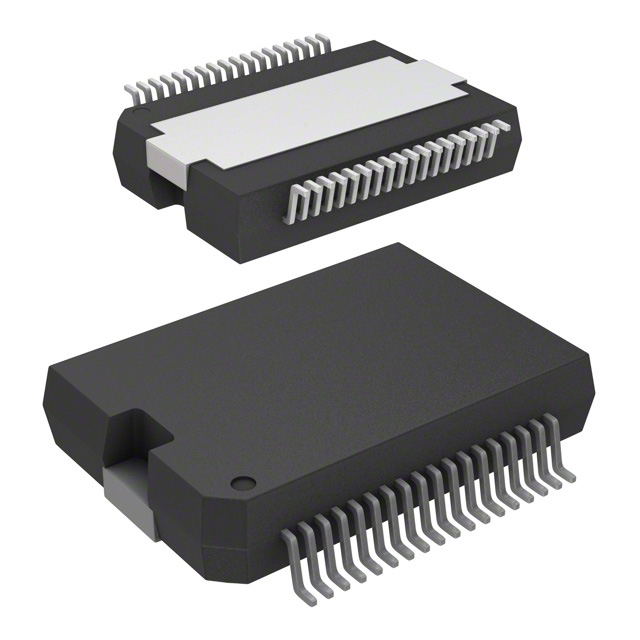
PG-DSO 36
General description
Six Channel Low-Side Switch in Smart Power Technology (SPT) with a Serial Peripheral Interface
(SPI) and six open drain DMOS output stages. The TLE 6232 GP is protected by embedded protection functions and designed for automotive and industrial applications. The output stages are controlled via an SPI Interface. Additionally all six channels can be controlled direct in parallel for PWM
applications. Therefore the TLE 6232 GP is particularly suitable for engine management and powertrain systems.
PRG
GND
RESET
VS
Block
Diagram
FAULT
VS
VBB
IN1
Protection
Functions
as Ch. 1
LOGIC
as Ch. 1
as Ch. 1
as Ch. 1
IN6
Output Stage
as Ch. 1
16
SCLK
SI
CS
OUT1
1
6
Serial Interface
SPI
6
Output Control
Buffer
6
OUT6
SO
GND
V2.3
Page
1
2009-11-18
�Data Sheet TLE 6232 GP
RESET FAULT
VS
Normal function
GND
VS
SCB/Overload/OT
PRG
Open load
IN1
IN2
as Ch.1
IN3
as Ch.1
IN4
as Ch.1
IN5
as Ch.1
IN6
as Ch.1
short to ground
Output Stage
OUT1
6
16
Channel 2
OUT2
Channel 3
OUT3
Channel 4
OUT4
Channel 5
OUT5
Channel 6
OUT6
SO
6
SI
SCLK
SPI
Interface
16 bit
Output
Control
Buffer
CS
GND
Detailed Block Diagram
V2.3
Page
2
2009-11-18
�Data Sheet TLE 6232 GP
Pin Description
Pin
1
2
3
4
5
6
7
8
9
10
11
12
13
14
15
16
17
18
19
20
21
22
23
24
25
26
27
28
29
30
31
32
33
34
35
36
Symbol
GND
NC
OUT5
NC
OUT1
IN5
IN1
Vs
RESET
CS
PRG
IN2
IN6
OUT2
NC
OUT6
NC
GND
GND
NC
NC
NC
OUT3
NC
IN3
FAULT
SO
SCLK
SI
IN4
NC
OUT4
NC
NC
NC
GND
Pin Configuration (Top view)
Function
Ground
not connected
Power Output Channel 5
not connected
Power Output Channel 1
Input Channel 5
Input Channel 1
Supply Voltage
Reset
Slave Select
Program (inputs high or low-active)
Input Channel 2
Input Channel 6
Power Output Channel 2
not connected
Power Output Channel 6
not connected
Ground
Ground
not connected
not connected
not connected
Power Output Channel 3
not connected
Input Channel 3
General Fault Flag
Serial Data Output
Serial Clock
Serial Data Input
Input Channel 4
not connected
Power Output Channel 4
not connected
not connected
not connected
Ground
GND
NC
OUT5
NC
OUT1
IN5
IN1
VS
RESET
CS
PRG
IN2
IN6
OUT2
NC
OUT6
NC
GND
1•
2
3
4
5
6
7
8
9
10
11
12
13
14
15
16
17
18
36 GND
35 NC
34 NC
33
NC
32 OUT4
31 NC
30 IN4
29
SI
28 SCLK
27
SO
26 FAULT
25 IN3
24 NC
23 OUT3
22
NC
21 NC
20 NC
19 GND
Power SO 36
Heat Slug internally connected to ground pins
V2.3
Page
3
2009-11-18
�Data Sheet TLE 6232 GP
Maximum Ratings for Tj = – 40°C to 150°C
Parameter
Supply Voltage
Continuous Drain Source Voltage (OUT1...OUT8)
Symbol
VS
VDS
Input Voltage, All Inputs and Data Lines
Operating Temperature Range
Storage Temperature Range
Output Current per Channel (see el. characteristics)
VIN
Tj
Tstg
ID(lim)
Single pulse inductive Energy (internal clamping)
Tj=125°C,
Ch1-4: 3A linear decreasing
Ch5,6: 1,5A linear decreasing
Output Current per Channel @ TA = 25°C
(All 6 Channels ON; Mounted on PCB ) 1)
Power Dissipation (mounted on PCB) @ TA = 25°C
E
Electrostatic Discharge Voltage (Human Body Model)
according to MIL STD 883D, method 3015.7 and EOS/ESD
assn. standard S5.1 - 1993
DIN Humidity Category, DIN 40 040
IEC Climatic Category, DIN IEC 68-1
Thermal Resistance
junction – case (die soldered on the frame)
junction - ambient @ min. footprint
junction - ambient @ 6 cm2 cooling area with heat pipes
ID 1-4
ID 5,6
Ptot
VESD
Values
-0.3 ... +7
45
- 0.3 ... + 7
- 40 ... + 150
- 55 ... + 150
ID(lim) min
Unit
V
V
V
°C
A
mJ
40
20
1.1
0.55
A
3.3
W
2000
V
E
40/150/56
RthJC
RthJA
2
50
38
K/W
PCB with heat pipes,
backside 6 cm2 cooling area
Minimum footprint
1)
Output current rating so long as maximum junction temperature is not exceeded. At TA = 125 °C the output
current has to be calculated using RthJA according mounting conditions.
V2.3
Page
4
2009-11-18
�Data Sheet TLE 6232 GP
Electrical Characteristics
Parameter and Conditions
VS = 4.5 to 5.5 V ; Tj = - 40 °C to + 150 °C ; Reset = H
(unless otherwise specified)
Symbol
Values
min
Unit
typ
max
1. Power Supply, Reset
Supply Voltage2
VS
4.5
--
5.5
V
Supply Current
IS
--
--
10
mA
Supply Current in Standby Mode (RESET = L)
Minimum Reset Duration
IS(stdy)
tReset,min
-1
---
10
--
µA
µs
RDS(ON)
---
0.25
--
0.28
0.5
Ω
RDS(ON)
---
0.45
--
0.55
1
Ω
VDS(AZ)
45
53
60
V
Current Limit Channel 1-4
ID(lim) 1-4
ID(lim) 5,6
4
2
6
3
A
Current Limit Channel 5,6
3
1.5
ID(lkg)
--
--
10
µA
2. Power Outputs
ON Resistance VS = 5 V; ID = 1 A
Channel 1-4
ON Resistance VS = 5 V; ID = 500 mA
TJ = 25°C
TJ = 150°C
TJ = 25°C
Channel 5,6
TJ = 150°C
Output Clamping Voltage
Output Leakage Current
Output OFF
VReset = L
Turn-On Time
Ch 1-4 ID = 2 A, resistive load
Ch 5,6 ID = 1 A, resistive load
tON
--
5
10
µs
Turn-Off Time
Ch 1-4 ID = 2 A, resistive load
Ch 5,6 ID = 1 A, resistive load
tOFF
--
5
10
µs
Switch-On Slew Rate (resistive load)
son
1
4
20
V/µs
Switch-Off Slew Rate (resistive load)
son
1
4
20
V/µs
3. Digital Inputs
Input Low Voltage
VINL
- 0.3
--
1.0
V
Input High Voltage
VINH
2.0
--
--
V
Input Voltage Hysteresis
Input Pull Down/Up Current (IN1 ... IN6)
Input Pull Up Current (Reset)
VINHys
IIN(1..6)
IIN(Res)
100
10
10
200
20
20
400
50
50
mV
µA
µA
Input Pull Down Current (PRG)
Input Pull Up Current ( CS , SI, SCLK)
IIN(PRG)
IIN(SI,SCLK)
10
10
20
20
50
50
µA
µA
VS - 1
--
--
V
4. Digital Outputs (SO, FAULT )
SO High State Output Voltage
SO Low State Output Voltage
ISOH = -2 mA
2 mA
VSOL
--
--
0.4
V
Output Tri-state Leakage Current CS = H, 0 ≤ VSO ≤ VS
FAULT Output Low Voltage
IFAULT = 2 mA
ISOlkg
-10
0
10
µA
VFAULTL
--
--
0.4
V
2
ISOL =
VSOH
For VS < 4.5V the power stages are switched according the input signals and data bits or are definitely switched
off. This under-voltage reset gets active at VS = 3V (typ. value) and is specified by design.
V2.3
Page
5
2009-11-18
�Data Sheet TLE 6232 GP
Electrical Characteristics cont.
Parameter and Conditions
Symbol
VS = 4.5 to 5.5 V ; Tj = - 40 °C to + 150 °C ; Reset = H
(unless otherwise specified)
5. Diagnostic Functions
Open Load Detection Voltage
VDS(OL)
Short to Ground Detection Voltage
VDS(SHG)
Values
Unit
min
typ
0.52*
0.6*
0.68*
Vs
Vs
Vs
0.32*
0.4*
0.48*
Vs
Diagnostic Current (incl. Leakage)
UOUTi,j = 14V
UOUTi,j = 0V
Current Limitation; Overload Threshold Current
Vs
max
V
V
Vs
IOUTi,j
-IOUTi,j
ID(lim) 1-4
ID(lim) 5,6
Tth(sd)
Thys
td(fault)
325
50
580
130
980
250
µA
µA
3
1.5
4
2
6
3
A
A
170
5
-10
200
20
°C
K
60
120
240
µs
fSCK
DC
200
50
100
100
------
5
-----
MHz
ns
ns
ns
ns
Enable Lag Time (falling edge of CLK to rising edge of CS ) tlag
Data Setup Time (required time SI to falling of CLK)
tSU
Data Hold Time (falling edge of CLK to SI)
tH
150
20
20
-----
----
ns
ns
ns
Disable Time
Transfer Delay Time3
( CS high time between two accesses)
Data Valid Time4
tDIS
--
--
100
ns
tdt
150
--
--
ns
tvalid
----
----
100
120
150
ns
ns
ns
Over-temperature Shutdown Threshold
Hysteresis
Fault Delay Time
6. SPI-Timing
Serial Clock Frequency (@ CSO ≤ 50pF)
Serial Clock Period (1/fclk)
Serial Clock High Time
Serial Clock Low Time
Enable Lead Time (falling edge of CS to rising edge of
CLK)
tp(SCK)
tSCKH
tSCKL
tlead
CL = 50 pF
CL = 100 pF
CL = 150 pF
3
This time is necessary between two write accesses. To get the correct diagnostic information, the transfer delay
time has to be extended to the maximum fault delay time td(fault)max = 200µs.
4
This parameter will not be tested but specified by design
V2.3
Page
6
2009-11-18
�Data Sheet TLE 6232 GP
Description of the Power Stages
4 low side power switches for nominal currents up to 3A (power stages OUT1 to OUT4). Control is possible by input pins or via SPI. For TJ = 150°C the on-resistance of the power
switches is below 500mΩ.
2 low side power switches for nominal currents up to 1.5A (power stages OUT5 and OUT6).
Control is possible by input pins or via SPI. For TJ = 150°C the on-resistance of the power
switches is below 1Ω.
In order to increase the switching current or to reduce the power dissipation parallel connection of power stages is possible.
Each of the 6 output stages is equipped with its own zener clamp, which limits the output voltage to a maximum of 60V. The outputs are provided with a current limitation set to a minimum
of 1.5A resp. 3A. Each power stage is equipped with an own temperature sensor.
Each output is protected by embedded protection functions5). In case of overload or shortcircuit to UBatt the current is internally limited and the corresponding bit combination is set
(early warning). If this operation leads to an over-temperature condition, a second protection
level (about 170°C) will change the output into a low duty cycle PWM (selective thermal shutdown with restart) to prevent critical chip temperatures.
The following faults can be detected (individually for each output):
- short to UBatt:
(SCB/overload) can be detected when switches are
- short to ground: (SCG) can be detected when switches are
- open load:
(OL) can be detected when switches are
- over-temperature: (OT) will only be detected when switches are
On state
Off state
Off state
On state
The fault conditions SCB, SCG and OL will not be stored until an integrated filtering time is
expired (please note for PWM application). If, at one output, several errors occur in a sequence, always the last detected error will be stored (with filtering time). All fault conditions
are encoded in two bits per switch and are stored in the corresponding SPI registers. Additionally there are two central diagnostic bits: one especially for over-temperature (latched result
of an OR-operation out of the 6 signals of the temperature sensor) and one for fault occurrence at any output. A fault that has been detected and stored in the fault register must not be
replaced by o.k.-state (11) unless it is read out by the RD_DIAG command sent by the microcontroller or an internal or external reset has been applied. I.e. the fault register will be
cleared only by the RD_DIAG command.
PRG - Program pin.
PRG = High (VS): Parallel inputs Channel 1 to 6 are high active
PRG = Low (GND): Parallel inputs Channel 1 to 6 are low active.
If the parallel input pins are not connected (independent of high or low activity), channels 1 to
6 are switched OFF.
PRG pin itself is internally pulled down when it is not connected.
5)
The integrated protection functions prevent device destruction under fault conditions and may not be used in
normal operation or permanently.
V2.3
Page
7
2009-11-18
�Data Sheet TLE 6232 GP
The effect of the integrated under-voltage detection is similar to the effect of an external reset
at pin Reset (except low current consumption):
- locks all power switches regardless of their input signals
- clears the fault registers
- resets SPI control register
Parallel Connection of Power Stages
The power stages which are connected in parallel have to be switched on and off simultaneously.
In case of overload the ground current and the power dissipation are increasing. The application has to take into account that all maximum ratings are observed (e.g. operating temperature TJ and total ground current IGND, see Maximal Ratings).
The maximum current limitation value (or overload detection threshold) of the parallel connected power stages is the summation of the corresponding maximum values of the power
stages (IOUT(lim)x + IOUT(lim)y + ....).
2 power stages of the
same type
(see note 1)
3 power stages of the
same type
(see note 1,2)
2 power stages with the
same clamping voltage,
but different nominal
current (see note 3)
Max. Nominal Current
Max. Clamping Energy
On Resistance
(Imax,OUTx+Imax,OUTy) x 0.9
0.8 x (Ex + Ey)
0.5 xRON ,OUTx , y
(Imax,OUTx+Imax,OUTy+
Imax,OUTz) x 0.8
0.7 x (Ex + Ey + Ez)
(Imax,OUTx+Imax,OUTy) x 0.8
Min (Eclpx , Eclpy)
0.34 xRON ,OUTx , y , z
RON ,OUTx xRON ,OUTy
RON ,OUTx + RON ,OUTy
Note 1: Power stages of the same type have the same nominal current
Note 2: Only for 3A power stages
Note 3: Parallel connection of power stage type 3A/53V with type 1.5A/53V
SPI Interface
The serial SPI interface makes possible communication between TLE6232 and the microcontroller.
TLE 6232 GP always works in slave mode whereas the microcontroller provides the master
function. The maximum baud rate is 5MBaud.
Applying a chip select signal at CS and setting bit 7 and bit 6 of the instruction byte to „1“ and
„0“ TLE 6232 GP is selected by the SPI master. SI is the data input (Signal In), SO the data
output
(Signal Out). Via SCLK (Serial Clock Input) the SPI clock is given by the master.
V2.3
Page
8
2009-11-18
�Data Sheet TLE 6232 GP
SPI Signal Description
CS - Chip Select. The system microcontroller selects the TLE 6232 GP by means of the CS
pin. Whenever the pin is in a logic low state, data can be transferred from the µC and vice
versa.
CS High to Low transition: - diagnostic status information is transferred from the power
outputs into the shift register.
- serial input data can be clocked in from then on
- SO changes from high impedance state to logic high or low
state corresponding to the SO bits
CS Low to High transition: - transfer of SI bits from shift register into output buffers
- reset of diagnosis register
To avoid any false clocking the serial clock input pin SCLK should be logic low state during
high to low transition of CS . When CS is in a logic high state, any signals at the SCLK and
SI pins are ignored and SO is forced into a high impedance state.
SCLK - Serial Clock. The system clock pin clocks the internal shift register of the TLE
6232 GP. The serial input (SI) accepts data into the input shift register on the falling edge of
SCLK while the serial output (SO) shifts diagnostic information out of the shift register on the
rising edge of serial clock. It is essential that the SCLK pin is in a logic low state whenever
chip select CS makes any transition. The number of clock pulses will be counted during a
chip select cycle. The received data will only be accepted, if exactly 16 clock pulses were
counted during CS is active.
SI - Serial Input. Serial data bits are shifted in at this pin, the most significant bit first. SI information is read in on the falling edge of SCLK. Input data is latched in the shift register and
then transferred to the control buffer of the output stages.
The input data consists of two bytes - a "control byte” followed by a "data byte". The control
byte contains the information as to whether the data byte will be accepted or ignored (see diagnostics section). The data byte contains the input information for the six channels. A logic
high level at this pin (within the data byte) will switch on the power switch, provided that the
corresponding parallel input is also switched on (AND-operation for channel 1 to 6).
SO - Serial Output. Diagnostic data bits are shifted out serially at this pin, the most significant
bit first. SO is in a high impedance state until the CS pin goes to a logic low state. New diagnostic data will appear at the SO pin following the rising edge of SCLK.
RESET - Reset pin. If the reset pin is in a logic low state, it clears the SPI shift register and
switches all outputs OFF. An internal pull-up structure is provided on chip.
In case of inactive chip select signal (High) or bit 7 and bit 6 of the instruction byte differing
from1“ and „0“ the data output SO remains into tri-state.
V2.3
Page
9
2009-11-18
�Data Sheet TLE 6232 GP
SPI Interface
Power Stages 1...6
Power Stages 1...6
SCON_REG
MUX_REG
CS
SCLK
CS
SPI Control:
SCK
SI
SO
State Machine
Clock Counter
Control Bits
Parity Generator
Shift Register
DIA_REG
Power Stages 1...6
SPI Communication
A SPI communication starts with a SPI instruction (SI control word) sent from the controller to
TLE 6232 GP. Simultaneously the device sends the first SO byte back to the µC.
During a writing cycle the controller sends the data after the SPI instruction, beginning with
the MSB. During a reading cycle, after having received the SPI instruction, TLE 6232 GP
sends the corresponding data to the controller, also starting with the MSB.
The SPI Interface consists of three register:
- MUX_REG: 8-bit (1 byte) length for parallel operation mode (IN1 ... IN6 enabled or not)
V2.3
Page
10
2009-11-18
�Data Sheet TLE 6232 GP
- SCON_REG: 8-bit (1 byte) length for serial control of the outputs (serial data bits)
- DIAG_REG: 16-bit (2 byte) length. Contains the diagnostic information (2 bits per channel), a common over-temperature bit and a common fault bit.
Registers MUX_REG and SCON_REG are writeable as well as readable from the microcontroller. The DIAG_REG can only be read from the µC.
This leads to five different control bytes which are recognized by the IC. The following table
shows the different modes.
MSB
WR_SCON
SI:
SO:
RD_SCON
SI:
SO:
WR_MUX
SI:
SO:
RD_MUX
SI:
SO:
RD_DIAG
SI:
SO
LSB
H L L H H L X X
Z Z F
OT DIA6 DIA5
H L L H L H X X
Z Z F
OT DIA6 DIA5
H L H L H L X X
Z Z F OT DIA6 DIA5
H L H L L H X X
Z Z F
OT DIA6 DIA5
H L L L L L X X
Z Z F
OT DIA6 DIA5
MSB
LSB
D6 D5 D4 D3 D2 D1 X X
DIA4
DIA3
DIA2
Write to SCON Register.
DIA1
X X X X X X X X
SCON6 .. . SCON1 H H
Read SCON Register
M6 M5 M4 M3 M2 M1 X X
Write to MUX Register.
DIA4 DIA3 DIA2 DIA1
X X X X X X X X Read MUX Register
MUX6 . . MUX1
H H
X X
DIA4
SI Control Byte
X X X X
DIA3 DIA2
X X Read DIAG Register
DIA1
SI Data Byte
Note:
’X’ means ’don’t care’, because data will be ignored
’Dx’ represents the serial data bits, either being H (= OFF) or L (= ON)
’Mx’ enables parallel control of channel x H (=parallel) or L (=serial)
’Z’ means tri-state
’F’ is the common fault flag
’OT’ is the common over-temperature flag
’DIAx’ is the 2 bit diagnosis information per channel
All other possible control bytes will lead to an ignorance of the data bits, but the full diagnosis
information (like RD_DIAG command) is provided at the SO line. A reset of all fault registers
(and OT bit) the will only be done if the RD_DIAG command was clocked in.
Characteristics of the SPI Interface
If the slave select signal at CS is High or bit 7 and bit 6 of the instruction byte differ from „1“
and „0“, the state machine is set on default condition, i.e. the state machine expects an instruction.
If the 5V-reset (RESET) is active, the SPI output SO is switched into tri-state.
In order to increase the possible number of SPI participants on one and the same CS signal,
bits 7 and 6 of the instruction byte are fixed as shown above. While receiving the first two bits
of the instruction byte the data output SO has to be in tri-state. After having received the first
two bits TLE6232 has to decide if it is addressed (bit 7 = high, bit 6 = low). In this case the
remaining 6 bits of the instruction byte and the data byte are accepted and the diagnostic
feedback respectively the data byte content (MUX, SCON) is sent to the microcontroller. Otherwise instruction and data bits are rejected and SO remains in tri-state.
V2.3
Page
11
2009-11-18
�Data Sheet TLE 6232 GP
On a reading access the bit pattern of the data byte at the SPI input SI will be ignored. The
first SO byte sent out simultaneously by the TLE 6232 GP always contains the common fault
bit, the over-temperature bit and the diagnostic information of channels 6 and 5 (2 bits each).
Depending on the SI control byte, the second SO byte contains the requested information.
- Read back of SCON_REG (SCON bits 6 to 1 and two high bits)
- Read back of MUX_REG (MUX information for channel 6 to 1 and two high bits)
- Diagnostic information of channel 4 to 1 (2 bits per channel)
On a writing access always the full diagnostic information of the 6 channels (2 bit per channel)
and the over-temperature and common fault bit is performed.
Invalid instruction/access:
An instruction is invalid, if the following condition is fulfilled:
- an unused instruction code is detected (see tables with SPI instructions).
If an invalid instruction is detected, a writing access on a register of TLE6232 GP is not allowwed. In addition an access is invalid if the number of SPI clock pulses counted during active
CS differs from exactly 16 clock pulses (falling edges are counted).
- On a writing access the received data is only taken over into the internal registers and
- the fault register is only cleared by the RD_DIAG command,
if exactly 16 SPI clock pulses were counted while CS active.
Writing access / 8 bit + 8 bit
resp.
SS
SPI Instruction
SI
1
0
-
-
-
-
-
Data/8 Bit
-
MSB
SO
MSB
Z Z F OT DIA6 DIA5
DIA4 DIA3 DIA2 DIA1
MSB
Reading access / 8 bit + 8 bit
SS
SI
1
0
SPI Instruction
- - - - -
XXXX XXXX
-
MSB
SO
V2.3
Data/8 Bit
Z Z F OT DIA6 DIA5
MSB
MSB
Page
12
2009-11-18
�Data Sheet TLE 6232 GP
Serial/Parallel Control of the Power Stages 1...6
(SPI-Instructions: WR_MUX, RD_MUX, WR_SCON, RD_SCON)
The following table shows the truth table for the control of the power stages 1...6. The register
MUX_REG prescribes parallel or serial control of the power stages. The register SCON_REG
prescribes the state of the power stage in case of serial control.
RST
0
1
1
1
1
1
1
PRG
X
X
X
0
0
1
1
INx
X
X
X
0
1
0
1
MUXx
X
0
0
1
1
1
1
SCONx
X
0
1
X
X
X
X
Output OUTx of Power Stage x, x = 1..6
OUTx off
Serial Control: OUTx on
Serial Control: OUTx off
Parallel Control: OUTx on
Parallel Control: OUTx off
Parallel Control: OUTx off
Parallel Control: OUTx on
Note: Serial Data bits are low active. Parallel Inputs are high or low active depending on the PRG pin.
Description of the SPI Registers
Register:
7
MUX6
State of
Reset:
Access by
Controller:
Bit
7
6
5
4
3
2
1-0
MUX_REG
6
MUX5
FFH
5
MUX4
3
MUX2
2
MUX1
1
1
0
1
1
1
0
1
Read/Write
Name
MUX6
MUX5
MUX4
MUX3
MUX2
MUX1
Register: SCON_REG
7
6
5
SCON6
SCON5
SCON4
State of
FFH
Reset:
Access by Read/Write
Controller:
Bit
Name
7
SCON6
6
SCON5
5
SCON4
4
SCON3
3
SCON2
2
SCON1
1-0
Diagnostics/Encoding of Failures
V2.3
4
MUX3
Description
Serial or parallel control of power stage 6
Serial or parallel control of power stage 5
Serial or parallel control of power stage 4
Serial or parallel control of power stage 3
Serial or parallel control of power stage 2
Serial or parallel control of power stage 1
No function: HIGH on reading
4
SCON3
3
SCON2
2
SCON1
Description
State of serial control of power stage 6
State of serial control of power stage 5
State of serial control of power stage 4
State of serial control of power stage 3
State of serial control of power stage 2
State of serial control of power stage 1
No function: HIGH on reading
Page
13
2009-11-18
�Data Sheet TLE 6232 GP
Description of the SPI Registers
(SPI Instructions: RD_DIAG)
Register: DIAG_REG1
7
6
5
ST7
ST6
ST5
State of
FFH
Reset:
Access by Read only
Controller:
Bit
Name
7-6
DIA4
5-4
DIA3
3-2
DIA2
1-0
DIA1
4
ST4
3
ST3
2
ST2
1
ST1
0
ST0
Description
Diagnostic Bits of power stage 4
Diagnostic Bits of power stage 3
Diagnostic Bits of power stage 2
Diagnostic Bits of power stage 1
Note:
This byte is always clocked out (second SO-byte), except the SI control words says:
RD_SCON or RD_MUX. But: The content of the fault register will only be deleted if the control command
’RD_DIAG’ was clocked in and 16 clock pulses were counted.
Register:
7
Z
State of
Reset:
Access by
Controller:
Bit
7-6
5
4
3-2
1-0
DIA_REG2
6
Z
FFH
5
F
4
OT
3
ST11
2
ST10
1
ST9
0
ST8
Read only
Name
Z
F
OT
DIA6
DIA5
Description
Bit 7 and 6 are always tri-state
Common error flag
Common over-temperature flag
Diagnostic Bits of power stage 6
Diagnostic Bits of power stage 5
Encoding of the Diagnostic (Status) Bits of the Power Stages
ST(2*x-1)
ST(2*x-2)
State of power stage x
x = 1..6
1
1
Power stage o.k.
1
0
Overload, short circuit to battery (SCB) or over-temperature (OT)
0
1
Open load (OL)
0
0
Short circuit to ground (SCG)
Note: DIA_REG2 is always clocked out as first byte
F, OT Bit = 1: No Fault
F, OT Bit = 0: Fault, Over-temperature
The over-temperature bit is the latched result of an OR-operation out of the 6 signals of
the temperature sensor)
The general fault bit shows the fault occurrence at any of the outputs.
Reset of the Diagnostic Information
The diagnostic information will only be reset after the RD_DIAG command on the rising edge
of slave select or a reset signal is applied (RESET = low).
V2.3
Page
14
2009-11-18
�Data Sheet TLE 6232 GP
Timing Diagrams
CS
SCLK
C
SI
O
N
T
R
O
L
Byte
7
6
5
4
10
9
8
7
6
5
4
3
2
1
2
1
MSB
15
SO
0
LSB
14
13
12
11
3
0
Figure 2: Serial Interface
CS
0.7VS
tdt
0.2 VS
tlag
trSI
tSCKH
tlead
0.7VS
SCLK
0.2VS
tSCKL
tSU
tH
tfSI
0.7VS
SI
0.2VS
Figure 3: Input Timing Diagram
0.7 VS
CS
SCLK
0.2 V S
tvalid
tDis
0.7 VS
SO
SO
0.2 V S
SO
0.7 VS
0.2 V S
Figure 4:
SO Valid Time Waveforms
V2.3
Enable and Disable Time Waveforms
Page
15
2009-11-18
�Data Sheet TLE 6232 GP
VIN
t
tOFF
tON
VDS
80%
20%
t
Figure 5:
Power Outputs
Timing is valid for resistive load with parallel and serial control.
Rising edge of chip select initiates the switching
Application Circuits
VBB
VS = 5V
C
10k
PRG VS
OUT1
FAULT
OUT2
RESET
IN1
µC
e.g. C167
IN6
MTSR
SI
MRST
SO
CLK
CLK
P xy
CS
TLE
6232 GP
OUT6
GND
V2.3
Page
16
2009-11-18
�Data Sheet TLE 6232 GP
Parallel SPI Configuration
Engine Management Application
TLE 6232 GP in combination with TLE 6240 GP (16-fold switch) for relays and general purpose loads and TLE 6220 GP (quad switch) to drive the injector valves. This arrangement
covers the numerous loads to be driven in a modern Engine Management/Powertrain system.
From 26 channels in sum 18 can be controlled direct in parallel for PWM applications.
Injector 1
4
P x.1-4
4 PWM
Channels
MTSR
SI
SO
MRST
CLK
CS
CLK
P x.y
CS
4
TLE
6220 GP
Quad
Injector 2
Injector 3
Injector 4
6 PWM
Channels
P x.1-6
µC
SI
SO
C167
CLK
P x.y
CS
TLE
6232 GP
Hex
8
8 PWM
Channels
P x.1-8
SI
SO
CLK
P x.y
V2.3
CS
TLE
6240 GP
16-fold
Page
17
2009-11-18
�Data Sheet TLE 6232 GP
Package and Ordering Code
(All dimensions in mm)
PG-DSO 36
TLE 6232 GP
Green Product (RoHS compliant)
To meet the world-wide customer requirements for environmentally friendly products and to be compliant with government regulations the device is available as a green product. Green products are
RoHS-Compliant (i.e Pb-free finish on leads and suitable for Pb-free soldering according to
IPC/JEDEC J-STD-020).
V2.3
Page
18
2009-11-18
�Data Sheet TLE 6232 GP
Revision History
Version
V2.2 ->
V2.3
Date
18.11.2009
V2.1 ->
V2.2
Changes
Package changed to PG-DSO-36
Ordering Code / Q-Nr. removed
V2.0 ->
V2.1
05.04.2007
Layout Changes, correct green package name implemented P-DSO36-12 à PG-DSO-36-26
V1.2 ->
V2.0
05.03.2007
Changes to Green Product Version:
- AEC, RoHS Logo and Feature List content added
- Package Name P-DSO -> PG-DSO
- Change History added
- Disclaimer re-newed
V1.2
08.10.2003
Initial Version of “grey” product
V2.3
Page
19
2009-11-18
�Data Sheet TLE 6232 GP
Edition 2007-04-17
Published by
Infineon Technologies AG
81726 Munich, Germany
© 11/19/09 Infineon Technologies AG
All Rights Reserved.
Legal Disclaimer
The information given in this document shall in no event be regarded as a guarantee of conditions or characteristics. With respect to any examples or hints given herein, any typical values stated herein and/or any information
regarding the application of the device, Infineon Technologies hereby disclaims any and all warranties and liabilities of any kind, including without limitation, warranties of non-infringement of intellectual property rights of any
third party.
Information
For further information on technology, delivery terms and conditions and prices, please contact the nearest Infineon Technologies Office (www.infineon.com).
Warnings
Due to technical requirements, components may contain dangerous substances. For information on the types in
question, please contact the nearest Infineon Technologies Office.
Infineon Technologies components may be used in life-support devices or systems only with the express written
approval of Infineon Technologies, if a failure of such components can reasonably be expected to cause the
failure of that life-support device or system or to affect the safety or effectiveness of that device or system. Life
support devices or systems are intended to be implanted in the human body or to support and/or maintain and
sustain and/or protect human life. If they fail, it is reasonable to assume that the health of the user or other persons may be endangered.
V2.3
Page
20
2009-11-18
�


 工商网监
湘ICP备2023018690号
工商网监
湘ICP备2023018690号
