TLE9461-3ES V33
Lite CAN SBC Family
1
Overview
Features
Key Features
•
Very low quiescent current consumption in Stop- and Sleep Mode
•
Periodic Cyclic Wake in SBC Normal-, Stop- and Sleep Mode
•
Periodic Cyclic Sense in SBC Normal-, Stop- and Sleep Mode
•
Low-Drop Linear Voltage Regulator 3.3 V, 150 mA (250 mA peak) for main supply,
•
Low-Drop Linear Voltage Regulator 5 V, 100 mA, protection feature for off-board usage
•
High-Speed CAN transceiver supporting FD communication up to 5 Mbit/s and featuring CAN Partial
Networking & CAN FD tolerant mode according to ISO 11898-2:2016 & SAE J2284
•
Fully compliant to “Hardware Requirements for LIN, CAN and FlexRay Interfaces in Automotive
Applications” Revision 1.3, 2012-05-04
•
Charge pump-output for N-channel MOSFET reverse-polarity protection or load switch feature with
integrated spread spectrum modulation feature for optimum EMC performance
•
Universal High-Voltage Wake input for voltage level monitoring and wake-up detection
•
General Purpose High-Voltage in- and output (GPIO) configurable as Fail Output, Wake Input, Low-Side
switch or High-Side switch
•
High-Voltage Measurement function as alternative pin assignment
•
Fail Output for Fail-Safe signalization
•
Configurable wake-up sources
•
Reset & Interrupt outputs
•
Configurable timeout and window watchdog
•
Overtemperature and short circuit protection feature
•
Dedicated TEST pin for SBC Development Mode entry (watchdog counter stopped)
•
Software compatible to other SBC families TLE926x and TLE927x
•
Wide input voltage and temperature range
•
Optimized for Electromagnetic Compatibility (EMC) and low Electromagnetic Emission (EME)
•
Optimized for high immunity against Electromagnetic Interference (EMI)
•
AEC Qualified & Green Product (RoHS compliant)
Datasheet
www.infineon.com
1
Rev. 1.1
2019-09-27
�TLE9461-3ES V33
Lite CAN SBC Family
Overview
Scalable System Basis Chip (SBC) Family
•
Product family for complete scalable application coverage
•
Optimized feature set for optimal system design
•
Dedicated Data Sheets are available for all product variants
•
Complete compatibility (hardware- and software across the family)
•
Same PG-TSDSO-24-1 package with exposed pad (EP) for all product variants
•
CAN Partial Networking variants (-3ES)
•
Product variants for 5 V (TLE94xxyy) and 3.3 V (TLE94xxyyV33) output voltage for main regulator
•
Software compatible to other SBC families TLE926x and TLE927x
Potential applications
•
HVAC ECU and Control panel
•
Light Control Unit (LCU) for front, rear and ambient
•
Seat control module
•
Seat belt pretension
•
Steering column and steering lock
•
Closure (trunk, sliding door, etc.)
•
Gear shifters and selectors
•
Smart power distribution modules
Product validation
Qualified for automotive applications. Product validation according to AEC-Q100/101.
Description
The TLE9461-3ES V33 is a monolithically integrated circuit in an exposed pad PG-TSDSO-24-1 (150 mil) power
package. The device is designed for various CAN automotive applications as main supply for the
microcontroller and as interface for a CAN bus network.
To support these applications, the System Basis Chip (SBC) provides the main functions, such as a 3.3 V lowdropout voltage regulator (LDO) for e.g. a microcontroller supply, another 5 V low-dropout voltage regulator
with off-board protection for e.g. sensor supply, a HS-CAN transceiver supporting CAN FD and CAN Partial
Networking (incl. FD tolerant mode) for data transmission, a high-voltage GPIO with embedded protective
functions and a 16-bit Serial Peripheral Interface (SPI) to control and monitor the device. Also a configurable
timeout / window watchdog circuit with a reset feature, one dedicated fail output and an undervoltage reset
feature are implemented.
The device offers low-power modes in order to minimize current consumption in applications that are
connected permanently to the battery. A wake-up from the low-power mode is possible via a message on the
CAN bus, via the bi-level sensitive monitoring/wake-up input as well as via Cyclic Wake.
The device is designed to withstand the severe conditions of automotive applications
Type
Package
Marking
TLE9461-3ES V33
PG-TSDSO-24-1
TLE9461-3ESV33
Datasheet
2
Rev. 1.1
2019-09-27
�TLE9461-3ES V33
Lite CAN SBC Family
Table of Contents
1
Overview . . . . . . . . . . . . . . . . . . . . . . . . . . . . . . . . . . . . . . . . . . . . . . . . . . . . . . . . . . . . . . . . . . . . . . . 1
2
Block Diagram . . . . . . . . . . . . . . . . . . . . . . . . . . . . . . . . . . . . . . . . . . . . . . . . . . . . . . . . . . . . . . . . . . . 7
3
3.1
3.2
3.3
3.4
Pin Configuration . . . . . . . . . . . . . . . . . . . . . . . . . . . . . . . . . . . . . . . . . . . . . . . . . . . . . . . . . . . . . . . . . 8
Pin Assignment . . . . . . . . . . . . . . . . . . . . . . . . . . . . . . . . . . . . . . . . . . . . . . . . . . . . . . . . . . . . . . . . . . . . . . . . . . . 8
Pin Definitions and Functions . . . . . . . . . . . . . . . . . . . . . . . . . . . . . . . . . . . . . . . . . . . . . . . . . . . . . . . . . . . . . . 8
Hints for Unused Pins . . . . . . . . . . . . . . . . . . . . . . . . . . . . . . . . . . . . . . . . . . . . . . . . . . . . . . . . . . . . . . . . . . . . 10
Hints for Alternative Pin Functions . . . . . . . . . . . . . . . . . . . . . . . . . . . . . . . . . . . . . . . . . . . . . . . . . . . . . . . . 10
4
4.1
4.2
4.3
4.4
General Product Characteristics . . . . . . . . . . . . . . . . . . . . . . . . . . . . . . . . . . . . . . . . . . . . . . . . . . .
Absolute Maximum Ratings . . . . . . . . . . . . . . . . . . . . . . . . . . . . . . . . . . . . . . . . . . . . . . . . . . . . . . . . . . . . . . .
Functional Range . . . . . . . . . . . . . . . . . . . . . . . . . . . . . . . . . . . . . . . . . . . . . . . . . . . . . . . . . . . . . . . . . . . . . . . .
Thermal Resistance . . . . . . . . . . . . . . . . . . . . . . . . . . . . . . . . . . . . . . . . . . . . . . . . . . . . . . . . . . . . . . . . . . . . . .
Current Consumption . . . . . . . . . . . . . . . . . . . . . . . . . . . . . . . . . . . . . . . . . . . . . . . . . . . . . . . . . . . . . . . . . . . .
11
11
13
14
15
5
5.1
5.1.1
5.1.1.1
5.1.1.2
5.1.2
5.1.3
5.1.4
5.1.5
5.1.6
5.1.7
5.1.8
5.2
5.2.1
5.2.1.1
5.2.1.2
5.2.2
5.2.3
5.3
5.3.1
5.4
5.4.1
5.4.2
5.4.3
5.5
5.6
5.6.1
5.6.2
5.6.2.1
5.6.2.2
5.6.2.3
5.6.2.4
5.6.3
System Features . . . . . . . . . . . . . . . . . . . . . . . . . . . . . . . . . . . . . . . . . . . . . . . . . . . . . . . . . . . . . . . .
Block Description of State Machine . . . . . . . . . . . . . . . . . . . . . . . . . . . . . . . . . . . . . . . . . . . . . . . . . . . . . . .
Device Configuration and SBC Init Mode . . . . . . . . . . . . . . . . . . . . . . . . . . . . . . . . . . . . . . . . . . . . . . . . .
Device Configuration . . . . . . . . . . . . . . . . . . . . . . . . . . . . . . . . . . . . . . . . . . . . . . . . . . . . . . . . . . . . . . . . .
SBC Init Mode . . . . . . . . . . . . . . . . . . . . . . . . . . . . . . . . . . . . . . . . . . . . . . . . . . . . . . . . . . . . . . . . . . . . . . .
SBC Normal Mode . . . . . . . . . . . . . . . . . . . . . . . . . . . . . . . . . . . . . . . . . . . . . . . . . . . . . . . . . . . . . . . . . . . . . .
SBC Stop Mode . . . . . . . . . . . . . . . . . . . . . . . . . . . . . . . . . . . . . . . . . . . . . . . . . . . . . . . . . . . . . . . . . . . . . . . .
SBC Sleep Mode . . . . . . . . . . . . . . . . . . . . . . . . . . . . . . . . . . . . . . . . . . . . . . . . . . . . . . . . . . . . . . . . . . . . . . .
SBC Restart Mode . . . . . . . . . . . . . . . . . . . . . . . . . . . . . . . . . . . . . . . . . . . . . . . . . . . . . . . . . . . . . . . . . . . . . .
SBC Fail-Safe Mode . . . . . . . . . . . . . . . . . . . . . . . . . . . . . . . . . . . . . . . . . . . . . . . . . . . . . . . . . . . . . . . . . . . .
SBC Development Mode . . . . . . . . . . . . . . . . . . . . . . . . . . . . . . . . . . . . . . . . . . . . . . . . . . . . . . . . . . . . . . . .
Electrical Characteristics for Pin TEST . . . . . . . . . . . . . . . . . . . . . . . . . . . . . . . . . . . . . . . . . . . . . . . . . . . .
Wake Features . . . . . . . . . . . . . . . . . . . . . . . . . . . . . . . . . . . . . . . . . . . . . . . . . . . . . . . . . . . . . . . . . . . . . . . . . .
Cyclic Sense . . . . . . . . . . . . . . . . . . . . . . . . . . . . . . . . . . . . . . . . . . . . . . . . . . . . . . . . . . . . . . . . . . . . . . . . . . .
Configuration and Operation of Cyclic Sense . . . . . . . . . . . . . . . . . . . . . . . . . . . . . . . . . . . . . . . . . . .
Cyclic Sense in Low-Power Mode . . . . . . . . . . . . . . . . . . . . . . . . . . . . . . . . . . . . . . . . . . . . . . . . . . . . . .
Cyclic Wake . . . . . . . . . . . . . . . . . . . . . . . . . . . . . . . . . . . . . . . . . . . . . . . . . . . . . . . . . . . . . . . . . . . . . . . . . . .
Internal Timer . . . . . . . . . . . . . . . . . . . . . . . . . . . . . . . . . . . . . . . . . . . . . . . . . . . . . . . . . . . . . . . . . . . . . . . . .
Charge Pump Output for Reverse Polarity Protection . . . . . . . . . . . . . . . . . . . . . . . . . . . . . . . . . . . . . . . .
Electrical Characteristics for Charge Pump . . . . . . . . . . . . . . . . . . . . . . . . . . . . . . . . . . . . . . . . . . . . . . .
High-Voltage Measurement Interface . . . . . . . . . . . . . . . . . . . . . . . . . . . . . . . . . . . . . . . . . . . . . . . . . . . . . .
Block Description . . . . . . . . . . . . . . . . . . . . . . . . . . . . . . . . . . . . . . . . . . . . . . . . . . . . . . . . . . . . . . . . . . . . . .
Functional Description . . . . . . . . . . . . . . . . . . . . . . . . . . . . . . . . . . . . . . . . . . . . . . . . . . . . . . . . . . . . . . . . .
Electrical Characteristics for Measurement Interface . . . . . . . . . . . . . . . . . . . . . . . . . . . . . . . . . . . . . .
Spread Spectrum Modulation Frequency Function . . . . . . . . . . . . . . . . . . . . . . . . . . . . . . . . . . . . . . . . . .
Partial Networking on CAN . . . . . . . . . . . . . . . . . . . . . . . . . . . . . . . . . . . . . . . . . . . . . . . . . . . . . . . . . . . . . . .
CAN Partial Networking - Selective Wake Feature . . . . . . . . . . . . . . . . . . . . . . . . . . . . . . . . . . . . . . . . .
SBC Partial Networking Function . . . . . . . . . . . . . . . . . . . . . . . . . . . . . . . . . . . . . . . . . . . . . . . . . . . . . . . .
Activation of SWK . . . . . . . . . . . . . . . . . . . . . . . . . . . . . . . . . . . . . . . . . . . . . . . . . . . . . . . . . . . . . . . . . . . .
Wake-up Pattern (WUP) . . . . . . . . . . . . . . . . . . . . . . . . . . . . . . . . . . . . . . . . . . . . . . . . . . . . . . . . . . . . . .
Wake-up Frame (WUF) . . . . . . . . . . . . . . . . . . . . . . . . . . . . . . . . . . . . . . . . . . . . . . . . . . . . . . . . . . . . . . .
CAN Protocol Error Counter . . . . . . . . . . . . . . . . . . . . . . . . . . . . . . . . . . . . . . . . . . . . . . . . . . . . . . . . . . .
Diagnoses Flags . . . . . . . . . . . . . . . . . . . . . . . . . . . . . . . . . . . . . . . . . . . . . . . . . . . . . . . . . . . . . . . . . . . . . . . .
19
20
21
21
24
25
26
27
28
29
30
32
33
33
34
37
37
38
39
40
41
41
41
43
44
45
45
46
47
48
48
49
50
Datasheet
3
Rev. 1.1
2019-09-27
�TLE9461-3ES V33
Lite CAN SBC Family
5.6.3.1
5.6.3.2
5.6.3.3
5.6.3.4
5.6.3.5
5.6.3.6
5.6.3.7
5.6.3.8
5.6.3.9
5.6.3.10
5.6.3.11
5.6.4
5.6.4.1
5.6.4.2
5.6.4.3
5.6.4.4
5.6.4.5
5.6.5
5.6.6
5.6.7
5.6.8
5.6.8.1
5.6.8.2
5.6.9
PWRON/RESET-FLAG . . . . . . . . . . . . . . . . . . . . . . . . . . . . . . . . . . . . . . . . . . . . . . . . . . . . . . . . . . . . . . . . .
BUSERR-Flag . . . . . . . . . . . . . . . . . . . . . . . . . . . . . . . . . . . . . . . . . . . . . . . . . . . . . . . . . . . . . . . . . . . . . . . .
TXD Dominant Time-out flag . . . . . . . . . . . . . . . . . . . . . . . . . . . . . . . . . . . . . . . . . . . . . . . . . . . . . . . . . .
WUP Flag . . . . . . . . . . . . . . . . . . . . . . . . . . . . . . . . . . . . . . . . . . . . . . . . . . . . . . . . . . . . . . . . . . . . . . . . . . .
WUF Flag (WUF) . . . . . . . . . . . . . . . . . . . . . . . . . . . . . . . . . . . . . . . . . . . . . . . . . . . . . . . . . . . . . . . . . . . . .
SYSERR Flag (SYSERR) . . . . . . . . . . . . . . . . . . . . . . . . . . . . . . . . . . . . . . . . . . . . . . . . . . . . . . . . . . . . . . .
Configuration Error . . . . . . . . . . . . . . . . . . . . . . . . . . . . . . . . . . . . . . . . . . . . . . . . . . . . . . . . . . . . . . . . . .
CAN Bus Timeout-Flag (CANTO) . . . . . . . . . . . . . . . . . . . . . . . . . . . . . . . . . . . . . . . . . . . . . . . . . . . . . . .
CAN Bus Silence-Flag (CANSIL) . . . . . . . . . . . . . . . . . . . . . . . . . . . . . . . . . . . . . . . . . . . . . . . . . . . . . . . .
SYNC-FLAG (SYNC) . . . . . . . . . . . . . . . . . . . . . . . . . . . . . . . . . . . . . . . . . . . . . . . . . . . . . . . . . . . . . . . . . . .
SWK_SET FLAG (SWK_SET) . . . . . . . . . . . . . . . . . . . . . . . . . . . . . . . . . . . . . . . . . . . . . . . . . . . . . . . . . . .
SBC Modes for Selective Wake (SWK) . . . . . . . . . . . . . . . . . . . . . . . . . . . . . . . . . . . . . . . . . . . . . . . . . . . . .
SBC Normal Mode with SWK . . . . . . . . . . . . . . . . . . . . . . . . . . . . . . . . . . . . . . . . . . . . . . . . . . . . . . . . . .
SBC Stop Mode with SWK . . . . . . . . . . . . . . . . . . . . . . . . . . . . . . . . . . . . . . . . . . . . . . . . . . . . . . . . . . . . .
SBC Sleep Mode with SWK . . . . . . . . . . . . . . . . . . . . . . . . . . . . . . . . . . . . . . . . . . . . . . . . . . . . . . . . . . . .
SBC Restart Mode with SWK . . . . . . . . . . . . . . . . . . . . . . . . . . . . . . . . . . . . . . . . . . . . . . . . . . . . . . . . . .
SBC Fail-Safe Mode with SWK . . . . . . . . . . . . . . . . . . . . . . . . . . . . . . . . . . . . . . . . . . . . . . . . . . . . . . . . .
Wake-up . . . . . . . . . . . . . . . . . . . . . . . . . . . . . . . . . . . . . . . . . . . . . . . . . . . . . . . . . . . . . . . . . . . . . . . . . . . . . .
Configuration for SWK . . . . . . . . . . . . . . . . . . . . . . . . . . . . . . . . . . . . . . . . . . . . . . . . . . . . . . . . . . . . . . . . . .
CAN Flexible Data Rate (CAN FD) Tolerant Mode . . . . . . . . . . . . . . . . . . . . . . . . . . . . . . . . . . . . . . . . . . .
Clock and Data Recovery . . . . . . . . . . . . . . . . . . . . . . . . . . . . . . . . . . . . . . . . . . . . . . . . . . . . . . . . . . . . . . .
Configuring the Clock Data Recovery for SWK . . . . . . . . . . . . . . . . . . . . . . . . . . . . . . . . . . . . . . . . . .
Setup of Clock and Data Recovery . . . . . . . . . . . . . . . . . . . . . . . . . . . . . . . . . . . . . . . . . . . . . . . . . . . . .
Electrical Characteristics . . . . . . . . . . . . . . . . . . . . . . . . . . . . . . . . . . . . . . . . . . . . . . . . . . . . . . . . . . . . . . .
50
50
50
50
50
50
51
51
51
51
51
52
52
53
54
55
56
56
56
57
58
58
59
60
6
6.1
6.2
6.3
Voltage Regulator 1 . . . . . . . . . . . . . . . . . . . . . . . . . . . . . . . . . . . . . . . . . . . . . . . . . . . . . . . . . . . . . .
Block Description . . . . . . . . . . . . . . . . . . . . . . . . . . . . . . . . . . . . . . . . . . . . . . . . . . . . . . . . . . . . . . . . . . . . . . . .
Functional Description . . . . . . . . . . . . . . . . . . . . . . . . . . . . . . . . . . . . . . . . . . . . . . . . . . . . . . . . . . . . . . . . . . .
Electrical Characteristics . . . . . . . . . . . . . . . . . . . . . . . . . . . . . . . . . . . . . . . . . . . . . . . . . . . . . . . . . . . . . . . . .
62
62
63
64
7
7.1
7.2
7.2.1
7.3
Voltage Regulator 2 . . . . . . . . . . . . . . . . . . . . . . . . . . . . . . . . . . . . . . . . . . . . . . . . . . . . . . . . . . . . . .
Block Description . . . . . . . . . . . . . . . . . . . . . . . . . . . . . . . . . . . . . . . . . . . . . . . . . . . . . . . . . . . . . . . . . . . . . . . .
Functional Description . . . . . . . . . . . . . . . . . . . . . . . . . . . . . . . . . . . . . . . . . . . . . . . . . . . . . . . . . . . . . . . . . . .
Short to Battery Protection . . . . . . . . . . . . . . . . . . . . . . . . . . . . . . . . . . . . . . . . . . . . . . . . . . . . . . . . . . . . .
Electrical Characteristics . . . . . . . . . . . . . . . . . . . . . . . . . . . . . . . . . . . . . . . . . . . . . . . . . . . . . . . . . . . . . . . . .
66
66
67
67
68
8
8.1
8.2
8.2.1
8.2.2
8.2.3
8.2.4
8.2.5
8.2.6
8.2.7
8.2.8
8.3
High-Speed CAN FD Transceiver . . . . . . . . . . . . . . . . . . . . . . . . . . . . . . . . . . . . . . . . . . . . . . . . . . .
Block Description . . . . . . . . . . . . . . . . . . . . . . . . . . . . . . . . . . . . . . . . . . . . . . . . . . . . . . . . . . . . . . . . . . . . . . . .
Functional Description . . . . . . . . . . . . . . . . . . . . . . . . . . . . . . . . . . . . . . . . . . . . . . . . . . . . . . . . . . . . . . . . . . .
CAN Off Mode . . . . . . . . . . . . . . . . . . . . . . . . . . . . . . . . . . . . . . . . . . . . . . . . . . . . . . . . . . . . . . . . . . . . . . . . . .
CAN Normal Mode . . . . . . . . . . . . . . . . . . . . . . . . . . . . . . . . . . . . . . . . . . . . . . . . . . . . . . . . . . . . . . . . . . . . .
CAN Receive Only Mode . . . . . . . . . . . . . . . . . . . . . . . . . . . . . . . . . . . . . . . . . . . . . . . . . . . . . . . . . . . . . . . .
CAN Wake Capable Mode . . . . . . . . . . . . . . . . . . . . . . . . . . . . . . . . . . . . . . . . . . . . . . . . . . . . . . . . . . . . . . .
CAN Bus termination . . . . . . . . . . . . . . . . . . . . . . . . . . . . . . . . . . . . . . . . . . . . . . . . . . . . . . . . . . . . . . . . . . .
TXD Time-out Feature . . . . . . . . . . . . . . . . . . . . . . . . . . . . . . . . . . . . . . . . . . . . . . . . . . . . . . . . . . . . . . . . . .
Bus Dominant Clamping . . . . . . . . . . . . . . . . . . . . . . . . . . . . . . . . . . . . . . . . . . . . . . . . . . . . . . . . . . . . . . . .
Undervoltage Detection . . . . . . . . . . . . . . . . . . . . . . . . . . . . . . . . . . . . . . . . . . . . . . . . . . . . . . . . . . . . . . . .
Electrical Characteristics . . . . . . . . . . . . . . . . . . . . . . . . . . . . . . . . . . . . . . . . . . . . . . . . . . . . . . . . . . . . . . . . .
71
71
71
73
73
74
74
75
75
76
76
77
9
High-Voltage Wake and Voltage Monitoring Input . . . . . . . . . . . . . . . . . . . . . . . . . . . . . . . . . . . . 84
Datasheet
4
Rev. 1.1
2019-09-27
�TLE9461-3ES V33
Lite CAN SBC Family
9.1
9.2
9.2.1
9.2.2
9.2.3
9.2.4
9.3
Block Description . . . . . . . . . . . . . . . . . . . . . . . . . . . . . . . . . . . . . . . . . . . . . . . . . . . . . . . . . . . . . . . . . . . . . . . .
High-Voltage Wake Function . . . . . . . . . . . . . . . . . . . . . . . . . . . . . . . . . . . . . . . . . . . . . . . . . . . . . . . . . . . . . .
Functional Description . . . . . . . . . . . . . . . . . . . . . . . . . . . . . . . . . . . . . . . . . . . . . . . . . . . . . . . . . . . . . . . . .
Wake Input Configuration . . . . . . . . . . . . . . . . . . . . . . . . . . . . . . . . . . . . . . . . . . . . . . . . . . . . . . . . . . . . . . .
Wake configuration for Cyclic Sense . . . . . . . . . . . . . . . . . . . . . . . . . . . . . . . . . . . . . . . . . . . . . . . . . . . . .
High-Voltage Sensing as Alternate Function . . . . . . . . . . . . . . . . . . . . . . . . . . . . . . . . . . . . . . . . . . . . . .
Electrical Characteristics . . . . . . . . . . . . . . . . . . . . . . . . . . . . . . . . . . . . . . . . . . . . . . . . . . . . . . . . . . . . . . . . .
10
10.1
10.2
Interrupt Function . . . . . . . . . . . . . . . . . . . . . . . . . . . . . . . . . . . . . . . . . . . . . . . . . . . . . . . . . . . . . . . 89
Block and Functional Description . . . . . . . . . . . . . . . . . . . . . . . . . . . . . . . . . . . . . . . . . . . . . . . . . . . . . . . . . 89
Electrical Characteristics . . . . . . . . . . . . . . . . . . . . . . . . . . . . . . . . . . . . . . . . . . . . . . . . . . . . . . . . . . . . . . . . . 91
11
11.1
11.1.1
11.1.2
11.1.3
11.2
Fail Output (FO) and General Purpose I/O (GPIO) . . . . . . . . . . . . . . . . . . . . . . . . . . . . . . . . . . . . .
Block and Functional Description . . . . . . . . . . . . . . . . . . . . . . . . . . . . . . . . . . . . . . . . . . . . . . . . . . . . . . . . .
Fail-Output Function . . . . . . . . . . . . . . . . . . . . . . . . . . . . . . . . . . . . . . . . . . . . . . . . . . . . . . . . . . . . . . . . . . .
General Purpose I/O Function as Alternative Function . . . . . . . . . . . . . . . . . . . . . . . . . . . . . . . . . . . . .
WK and FO/GPIO HV-Sensing Function as Alternative Function . . . . . . . . . . . . . . . . . . . . . . . . . . . . .
Electrical Characteristics . . . . . . . . . . . . . . . . . . . . . . . . . . . . . . . . . . . . . . . . . . . . . . . . . . . . . . . . . . . . . . . . .
12
12.1
12.1.1
12.1.2
12.2
12.2.1
12.2.2
12.2.3
12.2.4
12.2.5
12.3
12.4
12.4.1
12.4.2
12.5
12.5.1
12.5.2
12.6
12.7
12.8
12.8.1
12.8.2
12.8.3
12.9
Supervision Functions . . . . . . . . . . . . . . . . . . . . . . . . . . . . . . . . . . . . . . . . . . . . . . . . . . . . . . . . . .
Reset Function . . . . . . . . . . . . . . . . . . . . . . . . . . . . . . . . . . . . . . . . . . . . . . . . . . . . . . . . . . . . . . . . . . . . . . . . .
Reset Output Description . . . . . . . . . . . . . . . . . . . . . . . . . . . . . . . . . . . . . . . . . . . . . . . . . . . . . . . . . . . . . .
Soft Reset Description . . . . . . . . . . . . . . . . . . . . . . . . . . . . . . . . . . . . . . . . . . . . . . . . . . . . . . . . . . . . . . . . .
Watchdog Function . . . . . . . . . . . . . . . . . . . . . . . . . . . . . . . . . . . . . . . . . . . . . . . . . . . . . . . . . . . . . . . . . . . . .
Time-Out Watchdog . . . . . . . . . . . . . . . . . . . . . . . . . . . . . . . . . . . . . . . . . . . . . . . . . . . . . . . . . . . . . . . . . . .
Window Watchdog . . . . . . . . . . . . . . . . . . . . . . . . . . . . . . . . . . . . . . . . . . . . . . . . . . . . . . . . . . . . . . . . . . . .
Watchdog Setting Check Sum . . . . . . . . . . . . . . . . . . . . . . . . . . . . . . . . . . . . . . . . . . . . . . . . . . . . . . . . . .
Watchdog during SBC Stop Mode . . . . . . . . . . . . . . . . . . . . . . . . . . . . . . . . . . . . . . . . . . . . . . . . . . . . . . .
Watchdog Start in SBC Stop Mode due to Bus Wake . . . . . . . . . . . . . . . . . . . . . . . . . . . . . . . . . . . . . .
VS Power-On Reset . . . . . . . . . . . . . . . . . . . . . . . . . . . . . . . . . . . . . . . . . . . . . . . . . . . . . . . . . . . . . . . . . . . . .
VS Under- and Overvoltage . . . . . . . . . . . . . . . . . . . . . . . . . . . . . . . . . . . . . . . . . . . . . . . . . . . . . . . . . . . . . .
VS Undervoltage . . . . . . . . . . . . . . . . . . . . . . . . . . . . . . . . . . . . . . . . . . . . . . . . . . . . . . . . . . . . . . . . . . . . . .
VS Overvoltage . . . . . . . . . . . . . . . . . . . . . . . . . . . . . . . . . . . . . . . . . . . . . . . . . . . . . . . . . . . . . . . . . . . . . . .
VCC1 Over-/ Undervoltage and Undervoltage Prewarning . . . . . . . . . . . . . . . . . . . . . . . . . . . . . . . . . . .
VCC1 Undervoltage and Undervoltage Prewarning . . . . . . . . . . . . . . . . . . . . . . . . . . . . . . . . . . . . . . .
VCC1 Overvoltage . . . . . . . . . . . . . . . . . . . . . . . . . . . . . . . . . . . . . . . . . . . . . . . . . . . . . . . . . . . . . . . . . . . . .
VCC1 Short Circuit Diagnostics . . . . . . . . . . . . . . . . . . . . . . . . . . . . . . . . . . . . . . . . . . . . . . . . . . . . . . . . . . .
VCC2 Undervoltage and VCAN Undervoltage . . . . . . . . . . . . . . . . . . . . . . . . . . . . . . . . . . . . . . . . . . . . . .
Thermal Protection . . . . . . . . . . . . . . . . . . . . . . . . . . . . . . . . . . . . . . . . . . . . . . . . . . . . . . . . . . . . . . . . . . . . .
Individual Thermal Shutdown . . . . . . . . . . . . . . . . . . . . . . . . . . . . . . . . . . . . . . . . . . . . . . . . . . . . . . . . .
Temperature Prewarning . . . . . . . . . . . . . . . . . . . . . . . . . . . . . . . . . . . . . . . . . . . . . . . . . . . . . . . . . . . . . .
SBC Thermal Shutdown . . . . . . . . . . . . . . . . . . . . . . . . . . . . . . . . . . . . . . . . . . . . . . . . . . . . . . . . . . . . . . .
Electrical Characteristics . . . . . . . . . . . . . . . . . . . . . . . . . . . . . . . . . . . . . . . . . . . . . . . . . . . . . . . . . . . . . . . .
100
100
100
101
102
103
103
104
104
105
106
107
107
107
107
107
108
109
109
110
110
110
110
111
13
13.1
13.2
13.3
13.4
13.5
Serial Peripheral Interface . . . . . . . . . . . . . . . . . . . . . . . . . . . . . . . . . . . . . . . . . . . . . . . . . . . . . . .
SPI Block Description . . . . . . . . . . . . . . . . . . . . . . . . . . . . . . . . . . . . . . . . . . . . . . . . . . . . . . . . . . . . . . . . . . .
Failure Signalization in the SPI Data Output . . . . . . . . . . . . . . . . . . . . . . . . . . . . . . . . . . . . . . . . . . . . . . .
SPI Programming . . . . . . . . . . . . . . . . . . . . . . . . . . . . . . . . . . . . . . . . . . . . . . . . . . . . . . . . . . . . . . . . . . . . . . .
SPI Bit Mapping . . . . . . . . . . . . . . . . . . . . . . . . . . . . . . . . . . . . . . . . . . . . . . . . . . . . . . . . . . . . . . . . . . . . . . . .
SPI Control Registers . . . . . . . . . . . . . . . . . . . . . . . . . . . . . . . . . . . . . . . . . . . . . . . . . . . . . . . . . . . . . . . . . . . .
115
115
116
117
120
123
Datasheet
5
84
85
85
86
87
87
88
92
92
93
94
97
98
Rev. 1.1
2019-09-27
�TLE9461-3ES V33
Lite CAN SBC Family
13.5.1
13.5.2
13.6
13.6.1
13.6.2
13.6.3
13.7
General Control Registers . . . . . . . . . . . . . . . . . . . . . . . . . . . . . . . . . . . . . . . . . . . . . . . . . . . . . . . . . . . . . .
Selective Wake Control Registers . . . . . . . . . . . . . . . . . . . . . . . . . . . . . . . . . . . . . . . . . . . . . . . . . . . . . . .
SPI Status Information Registers . . . . . . . . . . . . . . . . . . . . . . . . . . . . . . . . . . . . . . . . . . . . . . . . . . . . . . . . .
General Status Registers . . . . . . . . . . . . . . . . . . . . . . . . . . . . . . . . . . . . . . . . . . . . . . . . . . . . . . . . . . . . . . .
Selective Wake Status Registers . . . . . . . . . . . . . . . . . . . . . . . . . . . . . . . . . . . . . . . . . . . . . . . . . . . . . . . .
Family and Product Information Register . . . . . . . . . . . . . . . . . . . . . . . . . . . . . . . . . . . . . . . . . . . . . . . .
Electrical Characteristics . . . . . . . . . . . . . . . . . . . . . . . . . . . . . . . . . . . . . . . . . . . . . . . . . . . . . . . . . . . . . . . .
126
138
150
151
158
160
161
14
14.1
14.2
14.3
14.4
Application Information . . . . . . . . . . . . . . . . . . . . . . . . . . . . . . . . . . . . . . . . . . . . . . . . . . . . . . . . .
Application Diagrams . . . . . . . . . . . . . . . . . . . . . . . . . . . . . . . . . . . . . . . . . . . . . . . . . . . . . . . . . . . . . . . . . . .
ESD Tests . . . . . . . . . . . . . . . . . . . . . . . . . . . . . . . . . . . . . . . . . . . . . . . . . . . . . . . . . . . . . . . . . . . . . . . . . . . . . .
Thermal Behavior of Package . . . . . . . . . . . . . . . . . . . . . . . . . . . . . . . . . . . . . . . . . . . . . . . . . . . . . . . . . . . .
Further Application Information . . . . . . . . . . . . . . . . . . . . . . . . . . . . . . . . . . . . . . . . . . . . . . . . . . . . . . . . .
163
163
169
170
171
15
Package Outlines . . . . . . . . . . . . . . . . . . . . . . . . . . . . . . . . . . . . . . . . . . . . . . . . . . . . . . . . . . . . . . . 172
16
Revision History . . . . . . . . . . . . . . . . . . . . . . . . . . . . . . . . . . . . . . . . . . . . . . . . . . . . . . . . . . . . . . . . 173
Datasheet
6
Rev. 1.1
2019-09-27
�TLE9461-3ES V33
Lite CAN SBC Family
Block Diagram
2
Block Diagram
VCP
VCC1
VIO
VS
VS
VIO
Charge
Pump
VS
VCC1
VS
Vint.
FO/GPIO
VS
VCC2
Alternative Function :
GPIO
SDI
SDO
CLK
SPI
CSN
VCC2
Fail Safe
SBC
STATE
MACHINE
TEST
Interrupt
Control
INTN
Watchdog
RESET
GENERATOR
RSTN
VCAN
WAKE
REGISTER
WK/VSENSE
TXDCAN
CAN cell
WK
Selective Wake
Logic
RXDCAN
CANH
CANL
GND
Figure 1
Datasheet
TLE9461-3ES V33 Block Diagram
7
Rev. 1.1
2019-09-27
�TLE9461-3ES V33
Lite CAN SBC Family
Pin Configuration
3
Pin Configuration
3.1
Pin Assignment
VCAN
TXDCAN
RXDCAN
CLK
SDI
SDO
CSN
INTN
RSTN
TEST
GND
VIO
24
1
23
2
22
3
21
4
TLE9461
20
5
6 Exposed 19
18
7
Die
Pad
17
8
16
9
15
10
14
11
13
12
Figure 2
Pin Configuration
3.2
Pin Definitions and Functions
CANL
CANH
GND
GND
VCC2
FO/GPIO
WK/VSENSE
VCP
VS
VS
n.c.
VCC1
Pin
Symbol
Function
1
VCAN
HS-CAN Supply Input; Supply needed for CAN Normal and Receive Only Mode
2
TXDCAN
Transmit CAN
3
RXDCAN
Receive CAN
4
CLK
SPI Clock Input
5
SDI
SPI Data Input; input for SBC (=MOSI)
6
SDO
SPI Data Output; output from SBC (=MISO)
7
CSN
SPI Chip Select Input; active low
8
INTN
Interrupt Output; used as wake-up flag for microcontroller in SBC Stop or
Normal Mode and for indicating failures. Active low.
During start-up used to set the SBC configuration in case of watchdog trigger
failure. External pull-up (typ. 47 kΩ) sets config 1/3, otherwise config 2/4 is
selected.
Datasheet
8
Rev. 1.1
2019-09-27
�TLE9461-3ES V33
Lite CAN SBC Family
Pin Configuration
Pin
Symbol
Function
9
RSTN
Reset Output; active low, internal pull-up
10
TEST
Test Pin; Connect to GND or leave open for normal user mode operation;
Connect to VCC1 at device power-on to activate SBC Development Mode
(see Chapter 5.1.7). Integrated pull-down resistor.
11
GND
Ground; LDO 1 Power GND
12
VIO
Digital I/O Pin Voltage Supply; Must be connected to the buffered VCC1 voltage
(see also Figure 50)
13
VCC1
Voltage Regulator 1 Output
14
n.c.
not connected; internally not bonded
15
VS
Supply Voltage; Supply for VCC1 power stage - both VS pins must be connected
together on same battery potential for proper operation; Connect to battery
voltage via reverse polarity protection diode and filter against EMC
16
VS
Supply Voltage; Main supply of device - both VS pins must be connected
together on same battery potential for proper operation; Connect to battery
voltage via reverse polarity protection diode and filter against EMC
17
VCP
Charge Pump Output; For driving the gate of external N-channel MOSFETs, e.g.
for reverse polarity protection or Kl.30 load switch. Always place a 1kΩ resistor
in series for protection
18
WK/VSENSE
Wake Input;
Sense Input; Alternative function: HV-measurement function input
19
FO/GPIO
Fail Output; Open Drain Output, active low;
GPIO; Alternative function: configurable pin as WK, LS-, or HS-witch supplied by
VS (default is FO, see also Chapter 11.1.1)
Sense Output; Alternative function: if HV-measurement function is configured
20
VCC2
Voltage Regulator 2 Output
21
GND
Ground; Analog GND
22
GND
Ground; CAN GND
23
CANH
CAN High Bus Pin
24
CANL
CAN Low Bus Pin
Cooling GND
Tab
Cooling Tab - Exposed Die Pad; For cooling purposes only, connect to but do not
use as an electrical ground1)
1) The exposed die pad at the bottom of the package allows better power dissipation of heat from the SBC via the PCB.
The exposed die pad is not connected to any active part of the IC. However, it should be connected to GND for the
best EMC performance.
Note:
Datasheet
Both VS Pins must be connected to same battery potential;
all GND pins as well as the Cooling Tab must be connected to one common GND potential
9
Rev. 1.1
2019-09-27
�TLE9461-3ES V33
Lite CAN SBC Family
Pin Configuration
3.3
Hints for Unused Pins
In case functions or pins are not used, it must be ensured that the configurations are done properly, e.g.
disabled via SPI. Unused pins should be handled as follows:
•
WK/VSENSE: connect to GND and disable WK inputs via SPI
•
RSTN / INTN / FO: leave open
•
VCC2: leave open and keep disabled
•
VCAN: connect to VCC1
•
CANH/L, RXDCAN, TXDCAN: leave all pins open
•
TEST: Leave open or connect to GND for normal user mode operation or connect to VIO to activate SBC
Development Mode;
•
n.c.: not connected; internally not bonded; leave open
•
If unused pins are routed to an external connector which leaves the ECU, then these pins should have
provision for a jumper (depopulated if unused)
3.4
Hints for Alternative Pin Functions
In case of SPI selectable alternative pin functions, it must be ensured that the correct configurations are also
selected via SPI (in case it is not done automatically). Please consult the respective chapter. In addition,
following topics shall be considered:
•
WK/VSENSE: The pin can be either used as high-voltage wake-up and monitoring function or for a voltage
measurement function (via bit setting WK_MEAS = ‘1’). In the second case, the WK pin shall not be used /
assigned for any wake-up detection nor Cyclic Sense functionality, i.e. WK must be disabled in the register
WK_CTRL_1 and the level information must be ignored in the register WK_LVL_STAT.
•
FO/GPIO: The pin can also be configured as a GPIO in the GPIO_CTRL register. In this case, the pin shall not
be used for any fail output functionality.
The default configuration after start-up or power on reset (POR) is FO.
Datasheet
10
Rev. 1.1
2019-09-27
�TLE9461-3ES V33
Lite CAN SBC Family
General Product Characteristics
4
General Product Characteristics
4.1
Absolute Maximum Ratings
Table 1
Absolute Maximum Ratings1)
Tj = -40°C to +150°C; all voltages with respect to ground, positive current flowing into pin
(unless otherwise specified)
Parameter
Symbol
Values
Min.
Typ.
Max.
Unit
Note or
Test Condition
Number
Voltages
Supply Voltage VS
VS, max
-0.3
–
28
V
–
P_4.1.1
Supply Voltage VS
VS, max
-0.3
–
40
V
Load Dump,
max. 400 ms
P_4.1.2
Voltage Regulator 1 Output
VCC1, max
-0.3
–
5.5
V
2)
P_4.1.3
Voltage Regulator 2 Output
VCC2, max
-0.3
–
28
V
VCC2 = 40 V for
Load Dump,
max. 400 ms;
P_4.1.5
Charge Pump Output
VCP, max
-0.3
–
VS
+ 16
V
Wake Input WK/VSENSE
VWK, max
-0.3
–
40
V
–
P_4.1.7
Fail Output FO/GPIO
VFO_TEST, max -0.3
–
VS
+ 0.3
V
–
P_4.1.8
CANH, CANL
VBUS, max
-27
–
40
V
–
P_4.1.9
Logic Input Pins (CSN, CLK,
SDI, TXDCAN, TEST)
VI, max
-0.3
–
VCC1
+ 0.3
V
–
P_4.1.10
Logic Output Pins (SDO,
RSTN, INTN, RXDCAN)
VO, max
-0.3
–
VCC1
+ 0.3
V
–
P_4.1.11
VCAN Input Voltage
VVCAN, max
-0.3
–
5.5
V
–
P_4.1.12
I/O Supply Voltage
VVIO, max
-0.3
–
5.5
V
Must be
connected to
VCC1
P_4.1.19
Maximum Differential CAN
Bus Voltage
VCAN_Diff, max -5
–
10
V
–
P_4.1.20
P_4.1.6
Temperatures
Junction Temperature
Tj
-40
–
150
°C
–
P_4.1.13
Storage Temperature
Tstg
-55
–
150
°C
–
P_4.1.14
VESD,11
-2
–
2
kV
HBM3)
ESD Susceptibility
ESD Resistivity
ESD Resistivity to GND,
CANH, CANL
Datasheet
VESD,12
-8
–
8
11
kV
4)3)
HBM
P_4.1.15
P_4.1.16
Rev. 1.1
2019-09-27
�TLE9461-3ES V33
Lite CAN SBC Family
General Product Characteristics
Table 1
Absolute Maximum Ratings1) (cont’d)
Tj = -40°C to +150°C; all voltages with respect to ground, positive current flowing into pin
(unless otherwise specified)
Parameter
ESD Resistivity to GND
ESD Resistivity Pin 1,
12,13,24 (corner pins) to
GND
Symbol
VESD,21
VESD,22
Values
Min.
Typ.
Max.
-500
–
500
-750
–
750
Unit
Note or
Test Condition
Number
V
CDM5)
P_4.1.17
V
5)
P_4.1.18
CDM
1)
2)
3)
4)
Not subject to production test, specified by design.
The VCC1 and digital I/O maximum rating can be 6.0 V for a limited time (up to 100h).
ESD susceptibility, HBM according to ANSI/ESDA/JEDEC JS-001 (1.5 kΩ, 100 pF)
Please see chapter “Application Information” For ESD “GUN” resistivity (according to IEC61000-4-2 “gun test” (150 pF,
330 Ω)).
5) ESD susceptibility, Charged Device Model “CDM” EIA/JESD22-C101 or ESDA STM5.3.1
Notes
1. Stresses above the ones listed here may cause permanent damage to the device. Exposure to absolute
maximum rating conditions for extended periods may affect device reliability.
2. Integrated protection functions are designed to prevent IC destruction under fault conditions described in the
data sheet. Fault conditions are considered as “outside” normal operating range. Protection functions are
not designed for continuous repetitive operation.
Datasheet
12
Rev. 1.1
2019-09-27
�TLE9461-3ES V33
Lite CAN SBC Family
General Product Characteristics
4.2
Functional Range
Table 2
Functional Range1)
Parameter
Symbol
Values
Min.
Typ.
Max.
Unit
Note or
Test Condition
Number
Supply Voltage
VS,func
VPOR
–
28
V
2)
CAN Supply Voltage
VCAN,func
4.75
–
5.25
V
–
SPI Frequency
fSPI
–
–
4
MHz
see
P_4.2.3
Chapter 13.7 for
fSPI,max
Junction Temperature
Tj
-40
–
150
°C
–
VPOR see section P_4.2.1
Chapter 12.9
P_4.2.2
P_4.2.4
1) Not subject to production test, specified by design.
2) Including Power-On Reset, Over- and Undervoltage Protection
Note:
Within the functional range the IC operates as described in the circuit description. The electrical
characteristics are specified within the conditions given in the related electrical characteristics
table.
Device Behavior Outside of Specified Functional Range:
•
28V < VS,func < 40V: Device is still functional (including the state machine); the specified electrical
characteristics might not be ensured anymore. The regulators VCC1/2 are working properly, however, a
thermal shutdown might occur due to high power dissipation. The specified SPI communication speed is
ensured; the absolute maximum ratings are not violated, however the device is not intended for
continuous operation of VS >28V. The device operation at high junction temperatures for long periods
might reduce the operating life time;
•
VCAN < 4.75V: The undervoltage bit VCAN_UV is set in the SPI register BUS_STAT and the transmitter is
disabled as long as the UV condition is present;
•
5.25V < VCAN < 6.0V: CAN transceiver is still functional. However, the communication might fail due to outof-spec operation;
•
VPOR,f < VS < 5.5V: Device is still functional; the specified electrical characteristics might not be ensured
anymore:
– The voltage regulators will enter the linear (RDS_On) operation mode ,
– A VCC1_UV reset could be triggered depending on the Vrtx settings,
– GPIO behavior depends on the respective configuration:
- HS/LS switches remain switched On as long as the control voltage is sufficient.
- An unwanted overcurrent shutdown may occur.
- OC shutdown bit set and the respective HS/LS switch will turn Off;
– FO output remains On if it was enabled before VS > 5.5V,
– The specified SPI communication speed is ensured.
Datasheet
13
Rev. 1.1
2019-09-27
�TLE9461-3ES V33
Lite CAN SBC Family
General Product Characteristics
4.3
Thermal Resistance
Table 3
Thermal Resistance1)
Parameter
Symbol
Junction to Soldering Point Rth(JSP)
Junction to Ambient
Rth(JA)
Values
Unit
Min.
Typ.
Max.
–
14
–
–
35
–
Note or
Test Condition
Number
K/W
Exposed Pad
P_4.3.1
K/W
2)
P_4.3.2
1) Not subject to production test, specified by design.
2) Specified Rth(JA) value is according to Jedec JESD51-2,-5,-7 at natural convection on FR4 2s2p board for a power
dissipation of 1.5W; the product (chip+package) was simulated on a 76.2x114.3x1.5mm3 with 2 inner copper layers
(2 x 70µm Cu, 2 x 35µm C); where applicable a thermal via array under the exposed pad contacted the first inner
copper layer and 300mm2 cooling areas on the top layer and bottom layers (70µm).
Datasheet
14
Rev. 1.1
2019-09-27
�TLE9461-3ES V33
Lite CAN SBC Family
General Product Characteristics
4.4
Current Consumption
Table 4
Current Consumption
Current consumption values are specified at Tj = 25°C, VS = 13.5 V, all outputs open (unless otherwise specified)
Parameter
Symbol
Values
Min.
Typ.
Max.
Unit Note or
Test Condition
Number
INormal
–
3.5
6.5
mA
VS = 5.5 V to 28 V;
Tj = -40 °C to +150 °C;
VCC2, CAN = Off
P_4.4.1
Stop Mode current
consumption
IStop_1,25
–
44
55
µA
1)
VCC2 & CAN2) = Off,
Cyclic Wake/Sense &
Watchdog = Off;
no load on VCC1;
I_PEAK_TH = ‘0’
P_4.4.2
Stop Mode current
consumption
IStop_1,85
–
50
72
µA
1)3)
Tj = 85°C;
VCC2 & CAN2) = Off;
Cyclic Wake/Sense &
Watchdog = Off;
no load on VCC1;
I_PEAK_TH = ‘0’
P_4.4.3
Stop Mode current
IStop_2,25
consumption
(high active peak threshold)
–
65
72
µA
1)
VCC2 & CAN2) = Off;
Cyclic Wake/Sense &
Watchdog = Off;
no load on VCC1;
I_PEAK_TH = ‘1’
P_4.4.4
Stop Mode current
IStop_2,85
consumption
(high active peak threshold)
–
70
92
µA
1)3)
Tj = 85°C;
VCC2 & CAN2)= Off;
Cyclic Wake/Sense &
Watchdog = Off;
no load on VCC1;
I_PEAK_TH = ‘1’
P_4.4.5
SBC Normal Mode
Normal Mode current
consumption
SBC Stop Mode
SBC Sleep Mode
Sleep Mode current
consumption
ISleep,25
–
15
25
µA
VCC2 & CAN2)= Off;
Cyclic Wake/Sense =
Off
P_4.4.6
Sleep Mode current
consumption
ISleep,85
–
25
35
µA
3)
P_4.4.7
Datasheet
15
Tj = 85°C;
VCC2 & CAN2) = Off;
Cyclic Wake/Sense =
Off
Rev. 1.1
2019-09-27
�TLE9461-3ES V33
Lite CAN SBC Family
General Product Characteristics
Table 4
Current Consumption (cont’d)
Current consumption values are specified at Tj = 25°C, VS = 13.5 V, all outputs open (unless otherwise specified)
Parameter
Symbol
Values
Min.
Typ.
Max.
Unit Note or
Test Condition
Number
Feature Incremental Current Consumption
Current consumption for
ICAN,rec
CAN module, recessive state
–
2
3
mA
3)
SBC Normal/Stop
Mode; CAN Normal
Mode; VCC2
connected to VCAN;
VTXDCAN = VCC2; no
RL on CAN
P_4.4.8
Current consumption for
CAN module, dominant
state
ICAN,dom
–
3
5
mA
3)
SBC Normal/Stop
Mode; CAN Normal
Mode; VCC1
connected to VCAN;
VTXDCAN = GND;
no RL on CAN
P_4.4.9
Current consumption for
CAN module, Receive Only
Mode
ICAN,RcvOnly
–
0.9
1.2
mA
3)4)
SBC Normal/Stop
Mode; CAN Receive
Only Mode; VCC1
connected to VCAN;
VTXDCAN = VCC1; no
RL on CAN
P_4.4.10
Current consumption during ICAN,SWK,25
CAN Partial Networking
frame detect mode
(RX_WK_ SEL = ‘0’)
–
360
470
µA
3)
Tj = 25°C;
SBC Stop Mode;
WK, VCC2 = Off;
CAN SWK Wake
Capable, SWK
Receiver enabled,
WUF detect;
no RL on CAN;
P_4.4.11
Current consumption during ICAN,SWK,85
CAN Partial Networking
frame detect mode
(RX_WK_ SEL = ‘0’)
–
390
500
µA
3)
Tj = 85°C;
SBC Stop Mode;
WK, VCC2 = Off;
CAN SWK Wake
Capable, SWK
Receiver enabled,
WUF detect;
no RL on CAN;
P_4.4.12
Current consumption for
WK, GPIO wake capability
(all wake inputs)
–
0.2
2
µA
5)6)7)
Datasheet
IWake,WK,25
16
SBC Sleep Mode; P_4.4.13
WK wake capable;
no activity on WK pin;
CAN = Off; VCC2 = Off
Rev. 1.1
2019-09-27
�TLE9461-3ES V33
Lite CAN SBC Family
General Product Characteristics
Table 4
Current Consumption (cont’d)
Current consumption values are specified at Tj = 25°C, VS = 13.5 V, all outputs open (unless otherwise specified)
Parameter
Symbol
Values
Min.
Typ.
Max.
Unit Note or
Test Condition
Number
3)5)6)7)
Current consumption for
WK, GPIO wake capability
(all wake inputs)
IWake,WK,85
–
0.5
3
µA
SBC Sleep Mode; P_4.4.14
Tj = 85°C;
WK wake capable;
no activity on WK pin;
CAN = Off; VCC2 = Off
Current consumption for
CAN wake capability
(tsilence expired)
IWake,CAN,25
–
4.5
6
µA
2)5)
SBC Sleep Mode;
CAN Wake Capable;
WK = Off; VCC2 = Off;
P_4.4.15
Current consumption for
CAN wake capability
(tsilence expired)
IWake,CAN,85
–
5.5
7
µA
2)3)5)
SBC Sleep Mode;
Tj = 85°C;
CAN Wake Capable;
WK = Off; VCC2 = Off;
P_4.4.16
VCC2 Normal Mode current
consumption
INormal,VCC2
–
2.5
3.5
mA
VS = 5.5 V to 28 V;
Tj = -40 °C to +150 °C;
VCC2 = On (no load)
P_4.4.17
Current consumption for
VCC2 in SBC Sleep Mode
ISleep,VCC2,25 –
25
35
µA
1)5)
SBC Sleep Mode;
VCC2 = On (no load);
CAN, WK = Off
P_4.4.18
Current consumption for
VCC2 in SBC Sleep Mode
ISleep,VCC2,85 –
30
40
µA
1)3)5)
SBC Sleep Mode;
Tj = 85°C; VCC2 = On
(no load);
CAN, WK = Off
P_4.4.19
Current consumption for
GPIO if configured as lowside / high-side in SBC Stop
Mode
IStop,GPIO,25
–
400
550
µA
3)5)
Current consumption for
GPIO if configured as lowside / high-side in SBC Stop
Mode
IStop,GPIO,85
–
450
600
µA
3)5)
P_4.4.21
SBC Stop Mode;
Tj = 85°C;
GPIO configured as HS
or LS with 100% duty
cycle (no load);
CAN, WK = Off
Current consumption for
Cyclic Sense function
IStop,CS25
–
20
26
µA
5)8)9)
SBC Stop Mode;
WD = Off;
P_4.4.22
Current consumption for
Cyclic Sense function
IStop,CS85
–
24
35
µA
3)5)8)9)
P_4.4.23
Datasheet
17
P_4.4.20
SBC Stop Mode;
GPIO configured as HS
or LS with 100% duty
cycle (no load);
CAN, WK = Off
SBC Stop Mode;
Tj = 85°C;
WD = Off;
Rev. 1.1
2019-09-27
�TLE9461-3ES V33
Lite CAN SBC Family
General Product Characteristics
Table 4
Current Consumption (cont’d)
Current consumption values are specified at Tj = 25°C, VS = 13.5 V, all outputs open (unless otherwise specified)
Parameter
Symbol
Values
Min.
Typ.
Max.
Unit Note or
Test Condition
Number
Current consumption for
watchdog active in Stop
Mode
IStop,WD25
–
20
26
µA
3)
SBC Stop Mode;
Watchdog running;
P_4.4.24
Current consumption for
watchdog active in Stop
Mode
IStop,WD85
–
24
35
µA
3)
P_4.4.25
SBC Stop Mode;
Tj = 85°C;
Watchdog running;
1) If the load current on VCC1 exceeds the configured VCC1 active peak threshold IVCC1,Ipeak1,r or IVCC1,Ipeak2,r, the current
consumption will increase by typ. 2.9mA to ensure optimum dynamic load behavior. Same applies to VCC2. See also
Chapter 6, Chapter 7.
2) CAN not configured in selective wake mode.
3) Not subject to production test, specified by design.
4) Current consumption adder also applies for WUF detection (frame detect mode) when CAN Partial Networking is
activated.
5) Current consumption adders of the features defined for SBC Stop Mode also apply for SBC Sleep Mode and vice versa.
The wake input signals are stable (i.e. not toggling), Cyclic Wake/Sense & watchdog are Off (unless otherwise
specified).
6) No pull-up or pull-down configuration selected.
7) The specified WK current consumption adder for wake capability applies regardless of how many WK inputs are
activated, i.e GPIO configured as wake input.
8) GPIO configured as HS used for Cyclic Sense, Timer with 20ms period, 0.1ms on-time, no load on GPIO.
In general the current consumption adder for Cyclic Sense in SBC Stop Mode can be calculated with below equation
(no load on FO/GPIO):
IStop,CS_typ = 18µA + (IStop,GPIO,25 × ton/TPer)
where 18uA is the base current consumption of the digital Cyclic Sense / wake-up functionality;
9) Also applies to Cyclic Wake but without the contribution of the HS biasing
Notes
1. There is no additional current consumption in SBC Normal Mode due to PWM generators or Timers.
2. To ensure the device functionality down to Vpor,f the quiescent current will increase gradually by ~35 uA for VS
< 9 V in SBC Stop Mode and Sleep Mode..
Datasheet
18
Rev. 1.1
2019-09-27
�TLE9461-3ES V33
Lite CAN SBC Family
System Features
5
System Features
This chapter describes the system features and behavior of the TLE9461-3ES V33:
•
State machine
•
Device configuration
•
SBC mode control
•
State of supplies and peripherals
•
System functions such as Cyclic Sense or Cyclic Wake
•
Charge pump output for reverse polarity protection and Kl. 30 load switching
•
High-voltage measurement interface
The System Basis Chip (SBC) offers six operating modes:
•
SBC Init Mode: Power-up of the device (initial and after a soft reset),
•
SBC Normal Mode: The main operating mode of the device,
•
SBC Stop Mode: The first-level power saving mode (the main voltage regulator VCC1 remains enabled),
•
SBC Sleep Mode: The second-level power saving mode (VCC1 is disabled),
•
SBC Restart Mode: An intermediate mode after a wake-up event from SBC Sleep or Fail-Safe Mode or after
a failure (e.g. WD failure, VCC1 under voltage reset) to bring the microcontroller into a defined state via a
reset. Once the failure condition is not present anymore the device will automatically change to SBC
Normal Mode after a delay time (tRD1 or tRD2).
•
SBC Fail-Safe Mode: A safe-state mode after critical failures (e.g. WD failure, VCC1 under voltage reset) to
bring the system into a safe state and to ensure a proper restart of the system later on. VCC1 is disabled. It
is a permanent state until either a wake-up event (via CAN, WK/VSENSE or GPIO configured as wake-up)
occurs or the over temperature condition is not present anymore.
A special mode, called SBC Development Mode, is available during software development or debugging of the
system. All above mentioned operating modes can be accessed in this mode. However, the watchdog counter
is stopped and does not need to be triggered. In addition, CAN is set to normal mode and VCC2 is On. This
mode can be accessed by connecting the TEST pin to VCC1 during SBC Init Mode.
The device can be configured via hardware to determine the device behavior after a watchdog trigger failure.
See Chapter 5.1.1 for further information.
The System Basis Chip is controlled via a 16-bit SPI interface. A detailed description can be found in
Chapter 13. The device configuration as well as the diagnosis is handled via the SPI. The SPI mapping of the
TLE9461-3ES V33 is compatible to other devices of the TLE926x and TLE927x families.
The device offers various supervision features to support functional safety requirements. Please see
Chapter 12 for more information.
Datasheet
19
Rev. 1.1
2019-09-27
�TLE9461-3ES V33
Lite CAN SBC Family
System Features
5.1
Block Description of State Machine
The different SBC operating modes are selected via SPI by setting the respective SBC MODE bits in the register
M_S_CTRL. The SBC MODE bits are cleared when going through SBC Restart Mode and thus always show the
current SBC mode.
First battery connection
SBC Soft Reset
Bit Locking Mechanism:
certain control bits, e.g. the
Charge Pump (CP) can be
locked and will not change
their configuration after a Soft
Reset command (stay fixed)
SBC Init Mode *
Config.: settings can be
changed in this SBC mode ;
(Long open window)
Fixed: settings stay as
defined in SBC Normal Mode
VCC1
ON
VCC2
OFF
FOx
inact.
CAN
OFF
SPI
WD
config. enabled
(3)
CP
Cyc. W/S
OFF/fixed
OFF
* The SBC Development
Mode is a super set of state
machine where the WD timer
is stopped , CAN & VCC2
behavior differs in SBC Init
Mode. Otherwise, there are
no differences in behavior .
Any SPI
command
SBC Normal Mode
Automatic
VCC1
ON
VCC2
config.
FOx
act/inact
CAN
config.
§ Reset is released
§ WD starts with long open window
SPI cmd
SPI
WD
config. config.
(3)
WD trigger
Cyc. W/S
CP
config. config.
SPI cmd
SPI cmd
SBC Stop Mode
SBC Sleep Mode
VCC1 over voltage
Config 1/3 (if VCC_OV_RST set)
Watchdog Failure:
Config 1/3 & 1st WD failure
in Config4
VCC2
fixed
FOx
fixed
CAN
(5)
Wake
capable /off
WD
OFF.
SPI
disabled
VCC1
ON
VCC2
fixed
CP
fixed
Cyc. W/S
FOx
fixed
CAN
fixed
fixed
(5)
WD
fixed
CP
fixed
SPI
enabled
Cyc. W/S
fixed
Wake up event
SBC Restart Mode
(RO pin is asserted)
VCC1
ON/
ramping
(6)
FOx
VCC1
Undervoltage
VCC1
OFF
active/
fixed
VCC2
OFF
CAN
(4)
woken /
OFF
WD
OFF
SPI
disabled
CP
fixed
Cyc. W/S
VCC1 over voltage
Config 2/4 (if VCC_OV_RST set)
SBC Sleep Mode entry
without any wake
source enabled
OFF
SBC Fail-Safe Mode
(1) After Fail-Safe Mode entry, the device will stay for at least typ . 1s
in this mode (with RO low) after a TSD2 event and min. typ. 100ms
after other Fail- Safe Events. Only then the device can leave the
mode via a wake-up event. Wake events are stored during this time.
CAN, WK or GPIO WK wake-up event
OR
Release of over temperature TSD2
after tTSD2
VCC1
OFF
(6)
FOx
active
VCC2
OFF
CAN
Wake
capable
(1)
WD
OFF
SPI
disabled
CP
fixed
Cyc. W/S
OFF
TSD2 event,
1st Watchdog Failure Config 2,
2nd Watchdog Failure, Config 4
VCC1 Short to GND
(3) For SBC Development Mode CAN/VCC2 are ON in SBC Init Mode
and stay ON when going from there to SBC Normal Mode
(4) See chapter CAN for detailed behavior in SBC Restart Mode
(5) CAN transceiver can be SWK capable, depending on configuration
(6) See Chapter 5.1.5 and 12.1 for detailed FOx behavior
Figure 3
Datasheet
State Diagram showing the SBC Operating Modes including CAN Partial Networking
20
Rev. 1.1
2019-09-27
�TLE9461-3ES V33
Lite CAN SBC Family
System Features
5.1.1
Device Configuration and SBC Init Mode
The device starts up in SBC Init Mode after crossing the power-on reset threshold VPOR,r (see also
Chapter 12.3) and the watchdog starts with a long open window (tLW) after RSTN is released (High level).
During this power-on phase the following configurations are stored in the device:
•
The device behavior regarding a watchdog trigger failure and a VCC1 over voltage condition is determined
by the external circuit on the INTN pin (typ. 47 kΩ pull-up resistor to VCC1, see also below)
•
The selection of the normal user mode operation or the SBC Development Mode (watchdog = Off, CAN =
On, VCC2 = On for debugging purposes) is set depending on the voltage level of the TEST pin (see also
Chapter 5.1.7).
5.1.1.1
Device Configuration
The configuration selection selects the SBC behavior due to a watchdog trigger failure and VCC1 overvoltage
detection. Depending on the requirements of the application, two different configurations can be chosen:
- If the VCC1 output shall be switched Off and the device shall go to SBC Fail-Safe Mode in case of a watchdog
failure (1 or 2 fails). To set this configuration (Config 2/4), the INTN pin does not need an external pull-up
resistor.
- If VCC1 should not be switched Off (Config 1/3), the INTN pin needs to have an external pull-up resistor
connected to VCC1 (see application diagram in Chapter 14).
Figure 4 shows the timing diagram of the hardware configuration selection. The hardware configuration is
defined during SBC Init Mode. The INTN pin is internally pulled Low with a weak pull-down resistor during the
reset delay time tRD1, i.e. after VCC1 crosses the reset threshold VRT1 and before the RSTN pin goes High. The
INTN pin is monitored during this time (with a continuous filter time of tCFG_F) and the configuration
(depending on the voltage level at INTN) is stored at the rising edge of RSTN.
Note:
If the POR bit is not cleared, then the internal pull-down resistor at INTN is reactivated every time
RSTN is pulled Low the configuration is updated at the rising edge of RSTN. Therefore it is
recommended to clear the POR bit right after initialization. In case there is no stable signal at INTN,
then the last filtered value is taken. If no filtered value is taken then the default value ‘0’ is taken as
the config select value (= SBC Fail-Safe Mode).
Note:
During device power up, the SPI status bits VCC1_ WARN, VCC1_UV and VS_UV are updated only if
RSTN is released after the reset delay time.
Datasheet
21
Rev. 1.1
2019-09-27
�TLE9461-3ES V33
Lite CAN SBC Family
System Features
VS
VPOR,r
t
VCC1
VRT1,r
t
RO
Continuous Filtering with t CFG_F
tRD1
t
Configuration selection monitoring period
Figure 4
Hardware Configuration Selection Timing Diagram
There are four different device configurations (Table 5) available defining the watchdog failure and the VCC1
over voltage behavior. The configurations can be selected via the external connection on the INTN pin and the
SPI bit CFG1 in the HW_CTRL_0 register (see also Chapter 13.4):
•
CFG0_STATE = ‘1’: Config 1 and Config 3:
– A watchdog trigger failure leads to SBC Restart Mode and depending on CFG1 the Fail Output (FO) is
activated after the 1st (Config 1) or 2nd (Config 3) watchdog trigger failure;
– A VCC1 over voltage detection leads to SBC Restart Mode if VCC1_OV_RST is set.
VCC1_ OV is set and the Fail Output is activated;
•
CFG0_STATE = ‘0’: Config 2 and Config 4:
– A watchdog trigger failure leads to SBC Fail-Safe Mode and depending on CFG1 the Fail Output (FO) is
activated after the 1st (Config 2) or 2nd (Config 4) watchdog trigger failure. The first watchdog trigger
failure in Config 4 leads to SBC Restart Mode;
– A VCC1 over voltage detection leads to SBC Fail-Safe Mode if VCC1_OV_RST is set.
VCC1_ OV is set and the Fail Output is activated;
The respective device configuration can be identified by reading the SPI bit CFG1 in the HW_CTRL_0 register
and the CFG0_STATE bit in the WK_LVL_STAT register.
Table 5 shows the configurations and the device behavior in case of a watchdog trigger failure:
Datasheet
22
Rev. 1.1
2019-09-27
�TLE9461-3ES V33
Lite CAN SBC Family
System Features
Table 5
Watchdog Trigger Failure Configuration
Config INTN Pin
(CFG0_STATE)
SPI Bit
CFG1
Event
FO Activation
SBC Mode Entry
1
External pull-up 1
1 x Watchdog Failure
after 1st WD Failure
SBC Restart Mode
2
No ext. pull-up
1 x Watchdog Failure
after 1st WD Failure
SBC Fail-Safe Mode
3
External pull-up 0
1 & 2 x Watchdog
Failure
after 2nd WD Failure SBC Restart Mode
4
No ext. pull-up
2 x Watchdog Failure
after 2nd WD Failure SBC Fail-Safe Mode1)
1
0
1) SBC Restart Mode is entered after the 1. watchdog failure. The 2nd watchdog failure leads to SBC Fail-Safe Mode
Table 6 shows the configurations and the device behavior in case of a VCC1 over voltage detection when
VCC1_OV_RST is set:
Table 6
Device Behavior in Case of VCC1 Over Voltage Detection
Config INTN Pin
CFG1
(CFG0_STATE) Bit
VCC1_O Event
V_RST
VCC1_ FO Activation
OV
SBC Mode Entry
1-4
any value
x
0
1 x VCC1 OV
1
no FO activation
unchanged
1
External pullup
1
1
1 x VCC1 OV
1
after 1st VCC1 OV
SBC Restart Mode
2
No ext. pull-up 1
1
1 x VCC1 OV
1
after 1st VCC1 OV
SBC Fail-Safe Mode
3
External pullup
0
1
1 x VCC1 OV
1
after 1st VCC1 OV
SBC Restart Mode
4
No ext. pull-up 0
1
1 x VCC1 OV
1
after 1st VCC1 OV
SBC Fail-Safe Mode
The respective configuration is stored for all conditions and can only be changed in SBC Init Mode, when RSTN
is ‘Low’ or by powering down the device (VS < VPOR,f) assuming the bit POR is cleared right after the device
power up (see also not on Page 21).
Datasheet
23
Rev. 1.1
2019-09-27
�TLE9461-3ES V33
Lite CAN SBC Family
System Features
5.1.1.2
SBC Init Mode
In SBC Init Mode, the device waits for the microcontroller to finish its startup and initialization sequence.
The SBC starts with a long open watchdog window (see also Chapter 12.2).
All diagnosis functions which are enabled by default at device power-up are active.
While in SBC Init Mode any valid SPI command (from the SPI protocol, i.e. 16-bit or 32-bit word) sets the device
to SBC Normal Mode, i.e. any register can be written, cleared and read. During the long open window the
watchdog has to be triggered (i.e. thereby the watchdog is automatically configured).
A missing watchdog trigger during the long open window will cause a watchdog failure and the device will
enter SBC Restart Mode.
Wake-up events are ignored during SBC Init Mode.
A SBC Soft Reset command (MODE = ‘11’) sets the SBC back into SBC Init Mode and the SPI registers are
changed to their respective Soft Reset values. In case one or both lock bits are set (CFG_LOCK_0 or
CFG_LOCK_1) the locked bits keep their previous values and stay unchanged.
Note:
Any SPI command sets the SBC to SBC Normal Mode even if it is an illegal SPI command (see
Chapter 13.2).
Note:
For a safe start-up, it is recommended to use the first SPI command to trigger and to configure the
watchdog (see Chapter 12.2).
Note:
At power up, the SPI bit VCC1_UV is not set nor is the FO triggered as long as VCC1 is below the VRT,x
threshold and VS is below the VS,UV threshold. The RSTN pin is kept Low as long as VCC1 is below the
selected VRT,x threshold and the reset delay time is not expired. After the first threshold crossing
(VCC1 > Vrt1,r) and the RSTN transition from Low to High, all subsequent undervoltage events lead
to SBC Restart Mode.
Note:
The bit VS_UV is updated only in SBC INIT Mode once RSTN resumes a high level.
Datasheet
24
Rev. 1.1
2019-09-27
�TLE9461-3ES V33
Lite CAN SBC Family
System Features
5.1.2
SBC Normal Mode
The SBC Normal Mode is the standard operating mode for the SBC. All remaining configurations must be done
in SBC Normal Mode before entering a low-power mode (see also Chapter 5.1.6). A wake-up event on CAN,
WK/VSENSE, FO/GPIO configured as wake input, the Timer will create an interrupt on pin INTN - however, no
change of the SBC mode will occur. The configuration options are listed below:
•
VCC1 is always active
•
VCC2 can be switched On or Off (default = Off)
•
CAN is configurable (it is Off coming from SBC Init Mode; Off or Wake Capable coming from SBC Restart
Mode, see also Chapter 5.1.5)
•
WK/VSENSE pin shows the input level and can be selected to be wake capable (interrupt), the alternative
measurement function with the voltage output at FO/GPIO can be activated by setting WK_MEAS
•
Cyclic Sense can be configured with the HS function of the GPIO (GPIO = ‘011’), WK/VSENSE input and
Timer
•
Cyclic Wake can be configured using the timer
•
Watchdog period is configurable
•
The Charge Pump Output can be switched On or Off (default = Off)
•
The FO/GPIO output is inactive by default. Coming from SBC Restart Mode and configured as FO it can be
active (due to a failure event, e.g. watchdog trigger failure, VCC1 short circuit, etc.) or inactive (no failure
occurred)
•
GPIO is configurable and is controlled by PWM; GPIO is Off coming from SBC Restart Mode
Certain SPI control bits with the bit type ‘rwl’ can be protected against unintentional modification by setting
the CFG_LOCK_1 bit in the register HW_CTRL_2. The locking mechanism stays activated until the device is
powered down (VS < VPOR,f). The charge pump and GPIO configuration can also be locked by setting the
CFG_LOCK_0 bit in the register HW_CTRL_1. The lock can be reset in SBC Normal Mode.
In SBC Normal Mode, the FO output can be tested within the system (i.e. to verify whether setting the FO/GPIO
pin to Low creates the intended behavior). The FO output can be enabled and then disabled again by the
microcontroller setting or resetting the FO_ON SPI bit. This feature is only intended for testing purposes.
Datasheet
25
Rev. 1.1
2019-09-27
�TLE9461-3ES V33
Lite CAN SBC Family
System Features
5.1.3
SBC Stop Mode
The SBC Stop Mode is the first level technique to reduce the overall current consumption by setting the
voltage regulators VCC1, VCC2 into a low-power mode. In this mode VCC1 is still active, supplying the
microcontroller, which can enter a power-down mode. The VCC2 supply can be configured to stay enabled
and CAN to stay in Normal Mode. All settings have to be done before entering SBC Stop Mode. In SBC Stop
Mode all SPI WRITE commands are ignored and the SPI_FAIL bit is set. Exceptions are changing to SBC Normal
Mode, triggering a SBC Soft Reset, refreshing the watchdog as well as reading and clearing the SPI status
registers. A wake-up event on CAN, WK/VSENSE, FO/GPIO (if configured as wake input) and Timer create an
interrupt on pin INTN - however, the SBC mode remains unchanged. The configuration options are listed
below:
•
VCC1 is always On
•
VCC2 is fixed as configured in SBC Normal Mode
•
CAN mode is fixed as configured in SBC Normal Mode
•
WK/VSENSE pin is fixed as configured in SBC Normal Mode
•
Cyclic Sense is fixed as configured in SBC Normal Mode
•
Cyclic Wake is fixed as configured in SBC Normal Mode
•
Watchdog is fixed as configured in SBC Normal Mode
•
SBC Soft Reset can be triggered
•
The Charge Pump state is fixed as configured in SBC Normal Mode
•
FO output works as configured in SBC Normal Mode unless it is changed by the software (i.e. by clearing
the FAILURE bit and triggering the watchdog properly)
•
GPIO is fixed as configured in SBC Normal Mode
If not all wake source signalization flags from WK_STAT_0 and WK_STAT_1 are cleared before entering SBC
Stop Mode, then an interrupt is triggered on the pin INTN.
Note:
If outputs are kept enabled during SBC Stop Mode, e.g. HS of GPIO, then the SBC current
consumption increases respectively (see Chapter 4.4).
Note:
It is not possible to switch directly from SBC Stop Mode to SBC Sleep Mode. Doing so sets the
SPI_FAIL flag and SBC into Restart Mode is entered.
Note:
When WK/VSENSE and FO/GPIO are configured for the alternative measurement function
(WK_MEAS = 1) the pins cannot be selected as wake input sources.
Datasheet
26
Rev. 1.1
2019-09-27
�TLE9461-3ES V33
Lite CAN SBC Family
System Features
5.1.4
SBC Sleep Mode
The SBC Sleep Mode is the second level technique to reduce the overall current consumption to a minimum
needed to react on wake-up events or for the SBC to perform autonomous actions (e.g. Cyclic Sense). In this
mode, VCC1 is Off, not supplying the microcontroller anymore. The VCC2 supply can be configured to stay
enabled. The settings have to be done before entering SBC Sleep Mode. A wake-up event on CAN, WK/VSENSE,
FO/GPIO (if configured as wake input) and the internal Timer brings the device via the SBC Restart Mode
subsequently to SBC Normal Mode again and signals the wake source.
The configuration options are listed below:
•
VCC1 is always Off
•
VCC2 is fixed as configured in SBC Normal Mode
•
CAN mode changes automatically from On or Receive Only Mode to Wake Capable mode or can be selected
to be Off
•
WK/VSENSE pin is fixed as configured in SBC Normal Mode
•
Cyclic Sense is fixed as configured in SBC Normal Mode
•
Cyclic Wake is fixed as configured in SBC Normal Mode, it can be the only activated wake source
•
Watchdog is Off
•
The Charge Pump state is fixed as configured in SBC Normal Mode
•
FO output is fixed as configured in SBC Normal Mode is maintained
•
GPIO is fixed as configured in SBC Normal Mode, it can be the only wake source if configured as WK/VSENSE
•
RSTN is pulled low
•
SPI communication and all digital I/Os are disabled because VCC1 is Off
•
The Sleep Mode entry is signalled in the SPI register DEV_STAT with the bit DEV_STAT
It is not possible to switch Off all wake sources in SBC Sleep Mode. Doing so sets the SPI_FAIL flag and the
device enters SBC Restart Mode.
In order to enter SBC Sleep Mode successfully, all wake source signalization flags from WK_STAT_0 and
WK_STAT_1 need to be cleared. A failure to do so results in an immediate wake-up from SBC Sleep Mode by
going via SBC Restart to Normal Mode.
All settings must be done before entering SBC Sleep Mode.
Note:
If outputs are kept enabled during SBC Sleep Mode, e.g. HS of GPIO, then the SBC current
consumption increases respectively (see Chapter 4.4).
Note:
The Cyclic Sense function might not work properly anymore in case of a failure event (e.g.
overcurrent, over temperature, reset) because the configured HS of the GPIO and Timer might be
disabled.
Note:
When WK/VSENSE and FO/GPIO are configured for the alternative measurement function
(WK_MEAS = 1) then the pins cannot be selected as wake input sources.
Datasheet
27
Rev. 1.1
2019-09-27
�TLE9461-3ES V33
Lite CAN SBC Family
System Features
5.1.5
SBC Restart Mode
There are multiple reasons to enter the SBC Restart Mode. The main purpose of the SBC Restart Mode is to
reset the microcontroller:
•
in case of under voltage at VCC1 in SBC Normal and SBC Stop Mode and SBC Init Mode after RSTN has been
released,
•
in case of over voltage at VCC1 (if the bit VCC1_OV_RST is set and if CFG0_STATE = ‘1’),
•
due to 1st incorrect Watchdog triggering (only if Config1, Config3 or Config 4 is selected, otherwise SBC
Fail-Safe Mode is immediately entered),
•
In case of a wake event from SBC Sleep or Fail-Safe Mode or a release of over temperature shutdown (TSD2)
out of SBC Fail-Safe Mode (this transition is used to ramp up VCC1 in a defined way).
From SBC Restart Mode, the device enters automatically to SBC Normal Mode. The SBC MODE bits are cleared.
As shown in Figure 37 the Reset Output (RSTN) is pulled Low when entering Restart Mode and is released
(going High) at the transition to SBC Normal Mode after the reset delay time (tRD1). The watchdog timer starts
with a long open window starting from the moment of the rising edge of RSTN. The watchdog period settings
in the register WD_CTRL are changed to the respective default value ‘100’.
Leaving the SBC Restart Mode does not result in changing / deactivating the Fail Output.
The behavior of the blocks is listed below:
•
FO (if configured as FO) is activated in case of a 1st watchdog trigger failure (Config1) or a 2nd watchdog
failure (Config3) or in case of VCC1 over voltage detection (if VCC1_OV_RST is set)
•
VCC1 stays On or is ramping up (coming from SBC Sleep or Fail-Safe Mode)
•
VCC2 is disabled if it was activated before
•
CAN is “woken” due to a wake-up event or Off depending on the previous SBC and transceiver mode (see
also Chapter 8). It is Wake Capable when it was in CAN Normal-, Receive Only or Wake Capable mode
before SBC Restart Mode
•
GPIO behavior: switched Off if configured as LS- or HS-switch, see also Chapter 11.1.2
•
RSTN is internally pulled Low during SBC Restart Mode
•
SPI communication is ignored by the SBC, i.e. it is not interpreted
•
The SBC Restart Mode entry is signalled in the SPI register DEV_STAT with the bits DEV_STAT
Table 7
Reasons for Restart - State of SPI Status Bits (after Return to SBC Normal Mode)
Prev. SBC Mode
Event
DEV_STAT WD_FAIL
VCC1_UV VCC1_OV
VCC1_SC
Normal
1x Watchdog Failure
01
01
x
x
x
Normal
2x Watchdog Failure
01
10
x
x
x
Normal
VCC1 under voltage reset 01
xx
1
x
x
Normal
VCC1 over voltage reset
01
xx
x
1
x
Stop
1x Watchdog Failure
01
01
x
x
x
Stop
2x Watchdog Failure
01
10
x
x
x
Stop
VCC1 under voltage reset 01
xx
1
x
x
Stop
VCC1 over voltage reset
01
xx
x
1
x
Sleep
Wake-up event
10
xx
x
x
x
Fail-Safe
Wake-up event
01
see “Reasons for Fail Safe, Table 8”
Datasheet
28
Rev. 1.1
2019-09-27
�TLE9461-3ES V33
Lite CAN SBC Family
System Features
Note:
An over voltage event at VCC1 leads to SBC Restart Mode only if the bit VCC1_OV_RST is set and if
CFG0_STATE = ‘1’ (Config 1/3).
Note:
The content of the WD_FAIL bits depends on the device configuration, e.g. 1 or 2 watchdog failures.
5.1.6
SBC Fail-Safe Mode
The purpose of this mode is to bring the system in a safe status after a failure condition by turning Off the VCC1
supply and powering Off the microcontroller. After a wake-up event the system restarts again.
The Fail-Safe Mode is automatically entered after following events:
•
SBC thermal shutdown (TSD2) (see also Chapter 12.8.3),
•
over voltage on VCC1 if the bit VCC1_OV_RST is set and if CFG0_STATE = ‘0’,
•
1st incorrect watchdog trigger in Config2 (CFG1 = 1) and after a 2nd incorrect watchdog trigger in Config4
(CFG1 = 0) (see also Chapter 5.1.1),
•
VCC1 is shorted to GND (see also Chapter 12.6),
In this case, the default wake sources CAN, WK/VSENSE and FO/GPIO (if configured as wake input - see also
registers BUS_CTRL_0, WK_CTRL_1 and GPIO_CTRL) are activated, the previous wake-up events are cleared
in the register WK_STAT_0 and WK_STAT_1, and both voltage regulators and the GPIO - if configured as HS or
LS - are switched Off.
The SBC Fail-Safe Mode is entered regardless of the FO/GPIO pin configuration. If WK/VSENSE and FO/GPIO are
configured for the alternative measurement function (WK_MEAS = 1) then these pins keep their configuration
for the measurement function when SBC Fail-Safe Mode is entered, i.e. they are not automatically activated
as wake sources.
The SBC Fail-Safe Mode is maintained until a wake-up event on the default wake sources occurs. To avoid any
fast toggling behavior a filter time of typ. 100ms (tFS,min) is implemented. Wake-up events during this time is
stored and automatically lead to SBC Restart Mode after the filter time.
In case of a VCC1 over temperature shutdown (TSD2), the SBC Restart Mode is entered automatically after a
filter time of typ. 1s (tTSD2) (without the need of a wake-up event) once the device temperature has fallen below
the TSD2 threshold. Please see Chapter 12.8.3 on how to extend the minimum TSD2 waiting time.
Leaving the SBC Fail-Safe Mode does not result in a deactivation of the Fail Output pins.
The following functions are controlled by the C Fail-Safe Mode:
•
FO output (if configured as FO) is activated (see also Chapter 11)
•
VCC1 is switched Off
•
VCC2 is switched Off
•
CAN is set to Wake Capable
•
GPIO behavior:
– if configured as HS or LS: it is switched Off
– if configured as wake input: it is set to wake capable in Static Sense mode
•
WK/VSENSE pin is set to wake capable in Static Sense mode (only if WK_MEAS = 0)
•
Cyclic Sense and Cyclic Wake is disabled
•
SPI communication is disabled because VCC1 is Off, RSTN and digital I/O pins are pulled Low
•
The Fail-Safe Mode activation is signalled in the SPI register DEV_STAT with the bits FAILURE and
DEV_STAT
Datasheet
29
Rev. 1.1
2019-09-27
�TLE9461-3ES V33
Lite CAN SBC Family
System Features
Table 8
Reasons for Fail-Safe - State of SPI Status Bits after Return to Normal Mode
Prev. SBC
Mode
Failure Event
DEV_
STAT
TSD2
WD_
FAIL
VCC1_
UV
VCC1_
OV
VCC1_
SC
Normal
1 x Watchdog Failure
01
x
01
x
x
x
Normal
2 x Watchdog Failure
01
x
10
x
x
x
Normal
TSD2
01
1
xx
x
x
x
Normal
VCC1 short to GND
01
x
xx
1
x
1
Normal
VCC1 over voltage
01
x
xx
x
1
x
Stop
1 x Watchdog Failure
01
x
01
x
x
x
Stop
2 x Watchdog Failure
01
x
10
x
x
x
Stop
TSD2
01
1
xx
x
x
x
Stop
VCC1 short to GND
01
x
xx
1
x
1
Stop
VCC1 over voltage
01
x
xx
x
1
x
Note:
An over voltage event on VCC1 leads to SBC Fail-Safe Mode only if the bit VCC1_OV_RST is set and if
CFG0_STATE = ‘0’ (Config 2/4).
Note:
The content of the WD_FAIL bits depends on the device configuration, e.g. 1 or 2 watchdog failures.
5.1.7
SBC Development Mode
The SBC Development Mode is used during the development phase of the module. It is especially useful for
software development.
Compared to the default SBC user mode operation, this mode is a super set of the state machine. The device
starts also in SBC Init Mode and it is possible to use all the SBC Modes and functions with the following
differences:
•
Watchdog is stopped and does not need to be triggered. Therefore no reset is triggered due to watchdog
failure
•
SBC Fail-Safe and SBC Restart Mode are not activated by a watchdog trigger failure (but the other reasons
to enter these modes are still valid)
•
CAN and VCC2 default values in SBC Init Mode and if entering SBC Normal Mode from SBC Init Mode is On
(instead of Off)
The SBC Development Mode is entered automatically, if the TEST pin is set High (i.e. connected to VCC1 with
(3.3V level) during SBC Init Mode. The voltage level monitoring is started as soon as VS > VPOR,r and VCC1 >
VRT1,r. The SBC Development Mode is set and maintained, if SBC Init Mode is left by sending any SPI command
while TEST is High. The bit SBC_DEV _LVL shows the status of the SBC Development Mode.
The Test pin has an integrated pull-down resistor, RTEST (switched On only during SBC Init Mode), to prevent
an unintentional SBC Development Mode entry (see also Figure 5).
Note:
Datasheet
The integrated pull-down resistor is disabled only, if the SBC Development Mode has been entered
successfully, i.e. not when the SBC Init Mode is left with an error (watchdog failure, VCC1
undervoltage reset, etc).
During normal user mode, the integrated pull-down resistor is always activated. In this case the
TEST pin can be left open or connect to GND
30
Rev. 1.1
2019-09-27
�TLE9461-3ES V33
Lite CAN SBC Family
System Features
Note:
In case a VCC2 overtemperature event occurs in SBC Init Mode., after SBC Development Mode is
entered, VCC2 is shut down.
TEST
SBC
Development
Mode
detection logic
Figure 5
RTEST
T test
Block Diagram of Pin TEST for SBC Development Mode Detection
In case the pin level toggles with a period faster than tTEST during the monitoring period the SBC Development
Mode is not reached .
The SBC remains in this mode for all operating conditions and can only be left by powering down the device
(VS < VPOR,f).
Note:
If the SBC enters SBC Fail-Safe Mode due to VCC1 shorted to GND during the SBC Init Mode, the SBC
Development is not entered and can only be activated at the next power-up of the SBC (after the
VCC1 short circuit is removed).
Note:
The absolute maximum ratings of the pin TEST must be observed. To increase the robustness of this
pin during debugging or programming a series resistor between TEST and the connector can be
added (see Figure 53).
Datasheet
31
Rev. 1.1
2019-09-27
�TLE9461-3ES V33
Lite CAN SBC Family
System Features
5.1.8
Electrical Characteristics for Pin TEST
Table 9
Electrical Characteristics1)
VS = 5.5 V to 28 V; Tj = -40°C to +150°C; SBC Normal Mode; all voltages with respect to ground; positive current
defined flowing into pin
(unless otherwise specified)
Parameter
Symbol
Values
Min.
Typ.
Max.
Unit
Note or
Test Condition
Number
Pull-down Resistance at
pin TEST
RTEST
7
10
13
kΩ
2)
VTEST = VCC1;
SBC Init Mode;
P_5.1.1
TEST Input Filter Time
tTEST
51
64
80
µs
3)
P_5.1.2
TEST High Input Voltage
Threshold
VTEST,IH
–
–
0.7 ×
VCC1
V
2)
P_5.1.3
TEST Low Input Voltage
Threshold
VITEST,IL
0.3 ×
VCC1
–
–
V
2)
P_5.1.4
TEST Hysteresis of Input
Voltage
VTEST,IHY 0.08 ×
VCC1
0.12 ×
VCC1
0.4 ×
VCC1
V
2)
P_5.1.5
1) The external capacitance on the TEST pin must be limited to less than 10nF to ensure proper detection of SBC
Development Mode and SBC User Mode operation.
2) Not subject to production test, specified by design.
3) Not subject to production test, tolerance defined by internal oscillator tolerance.
Datasheet
32
Rev. 1.1
2019-09-27
�TLE9461-3ES V33
Lite CAN SBC Family
System Features
5.2
Wake Features
The following wake sources are implemented in the device:
•
Static Sense: WK/VSENSE input and/or GPIO WK input are permanently active as a wake source, i.e WK_EN
is set and/or FO/GPIO is enabled as wake input (see Chapter 9.2.2 & Chapter 11.1.3)
•
Cyclic Sense: WK/VSENSE input only active during On-time of Cyclic Sense period. Internal timer is
activating GPIO HS during On-time for sensing the WK/VSENSE input (see Chapter 5.2.1)
•
Cyclic Wake: wake-up is controlled by internal timer, wake inputs are not used for Cyclic Wake (see
Chapter 5.2.2)
•
CAN wake: Wake-up via CAN message, i.e. CAN wake-up pattern (WUP, see also Chapter 8) or CAN wakeup frame (WUF, see also Chapter 5.6)
5.2.1
Cyclic Sense
The Cyclic Sense feature is intended to reduce the quiescent current of the device and the application.
In the Cyclic Sense configuration, the GPIO (configured as high-side driver) is switched On periodically,
controlled by TIMER_CTRL. The high-side switch supplies external circuitries e.g. switches and/or resistor
arrays, which are connected to the wake input WK (see Figure 6). Any edge change of the WK/VSENSE input
signal during the On-time of the Cyclic Sense period causes a wake-up. Depending on the SBC mode, either
the INTN is pulled Low (SBC Normal Mode and Stop Mode) or the SBC is woken enabling the VCC1 (after SBC
Sleep Mode).
FO/GPIO
GPIO
Config. as HS
GPIO_CTRL
10k
10k
WK/
VSENSE
WK
TIMER_CTRL
Period / On-Time
Signal
SBC
STATE
MACHINE
Switching
Circuitry
to uC
Figure 6
Datasheet
INTN
Cyclic Sense Working Principle
33
Rev. 1.1
2019-09-27
�TLE9461-3ES V33
Lite CAN SBC Family
System Features
5.2.1.1
Configuration and Operation of Cyclic Sense
The correct sequence to configure the Cyclic Sense is shown in Figure 7. All the configurations have to be
performed before the On-time is set in the TIMER_CTRL registers.
Cyclic Sense (=Timer) starts as soon as the respective On-time has been selected independently from the
assignment of the HS and the filter configuration.
The correct configuration sequence is as follows:
•
Configuring GPIO as HS with Cyclic Sense functionality
•
Enabling WK/VSENSE as wake source
•
Selecting the pull-up/down configuration, all configurations are valid for Cyclic Sense, recommended is
the automatic pull-up / down selection
•
Configuring the timer period and On-time
Cyclic Sense Configuration
Configure GPIO as HS with cyclic
sense function by setting
GPIO = ‚011' in GPIO_CTRL
GPIO_CTRL configure as HS
Enable WK as a wake source
WK_CTRL_1
WK_EN in WK_CTRL_1
Select WK pull-up / pull-down
configuration in WK_PUPD_CTRL
No pull-up/-down, pull-down or pull -up
selected, automatic switching
Select Timer Period and desired
On-Time in TIMER_CTRL
Period : 10, 20, 50, 100, 200 ms, 500ms, 1s, 2s,
5s, 10s, 20s, 50s, 100s, 200s, 500 s, 1000s
On-Time: 0.1, 0.3, 1.0, 10, 20ms
Cyclic Sense starts / ends by
setting / clearing On-time
A new timer configuration will become active
immediately , i.e. as soon as CSN goes high
Figure 7
Cyclic Sense: Configuration and Sequence
Note:
If the sequence is not ensured the Cyclic Sense function might not work properly, e.g. an interrupt
could be missed or an unintentional interrupt could be triggered. However, if Cyclic Sense is the only
wake source and configured properly (e.g. Timer not yet set), then SBC Restart Mode is entered
immediately because no valid wake source was set.
Note:
All configurations of period and On-time can be selected. However, recommended On-times for
Cyclic Sense are 0.1ms, 0.3ms and 1ms for quiescent current saving reasons. The SPI_FAIL is set if the
On-time is longer than the period.
Note:
A learning cycle is started every time when the timer is started via the On-time and GPIO is
configured as HS with Cyclic Sense = ‘011 (i.e. the Cyclic Sense function is enabled).
Datasheet
34
Rev. 1.1
2019-09-27
�TLE9461-3ES V33
Lite CAN SBC Family
System Features
The first sample of the WK/VSENSE input value (High or Low) is used as the reference for the next cycle. If a
change of the WK/VSENSE input level is detected during the On-time of the second or later cycle then a wakeup from SBC Sleep Mode or an interrupt during SBC Normal or SBC Stop Mode is triggered.
A filter time of 16µs is implemented to avoid a parasitic wake-up due to transients or EMI disturbances. The
filter time tFWK1 is triggered right at the end of the selected On-time and a wake signal is recognized if:
•
there was an input level change (crossing the switching threshold level VWKth) between the current and
previous cycle and
•
the input level did not change during the filter time
A wake-up event due to Cyclic Sense also sets the bit WK_WU.
During Cyclic Sense, WK_LVL_STAT is updated only with the sampled voltage levels of the WK/VSENSE pin in
SBC Normal or SBC Stop Mode.
Note:
In SBC Stop Mode the respective bits WK_WU and WK_LVL are only updated if the timer On-time is
configured for TIMER_ ON = '001'.
The functionality of the sampling and different scenarios are depicted in Figure 8 to Figure 10. The behavior
in SBC Stop and SBC Sleep Mode is identical except that in SBC Normal and Stop Mode INTN is triggered to
signal a change of WK/VSENSE input level and in SBC Sleep Mode, VCC1 will power-up instead. A wake-up
event is triggered regardless if the bit WK_WU is already set.
HS static ON
Cyclic Sense
Periode
GPIO HS
Filter time
tFWK1
Filter time
tFWK1
On Time
1st sample taken
as reference
Figure 8
Datasheet
Wake detection possible
on 2nd sample
Cyclic Sense Timing
35
Rev. 1.1
2019-09-27
�TLE9461-3ES V33
Lite CAN SBC Family
System Features
GPIO HS
Filter time
High
Low
Switch
Spike
open
closed
WK
High
Low
n-1
n
Learning
Cycle
WKn-1 = Low
INTN
n+1
WKn = Low
WKn = WKn-1
ðno wake event
High
WKn = WKn+1 = Low
(but ignored because
change during filter time )
WKn = WKn+1
ð no wake event
n+2
WKn+2= High
WKn+2 ≠WK n+1
ðwake event
Low
INTN &
WK Bit Set
Start of
Cyclic Sense
Figure 9
Cyclic Sense Example Timing for SBC Stop Mode, HS starts Low, GND based WK/VSENSE
input
GPIO HS
Filter time
High
Low
Switch
Spike
open
closed
WK
High
Low
n-1
VCC1
Learning
Cycle
WKn-1 = Low
High
n
WKn = Low
WKn = WK n-1
ðno wake event
n+1
WKn = WKn+1 = Low (but
ignored because change during
filter time), WKn = WKn+1
ð no wake event
Transition to SBC Normal
via Restart Mode
SBC Sleep Mode
Low
WK Bit Set
Start of
Cyclic Sense
Figure 10
Datasheet
n+2
WKn+2= High
WKn+2 ≠WK n+1
ðwake event
Cyclic Sense Example Timing for SBC Sleep Mode, HS starts with On,
GND based WK/VSENSE input
36
Rev. 1.1
2019-09-27
�TLE9461-3ES V33
Lite CAN SBC Family
System Features
The Cyclic Sense function is disabled at the following conditions (WK/VSENSE is automatically switched to
Static Sense):
•
in case SBC Fail-Safe Mode is entered: The HS GPIO switch is disabled and the wake pin is changed to static
sensing. An unintended wake-up event could be triggered when the WK/VSENSE input is changed to static
sensing.
•
In SBC Normal, Stop, or Sleep Mode in case of an overcurrent or overtemperature (TSD2) event: the HS
GPIO switch is disabled
Note:
The internal timer for Cyclic Sense is not cleared automatically in case the HS switch is turned Off due
to above mentioned failures. The timer is only cleared during SBC Restart Mode. This must be
considered to avoid a loss of wake-up events, especially before entering SBC Sleep Mode, i.e. the
software must ensure that at least another wake source is active or re-enable the GPIO HS again.
5.2.1.2
Cyclic Sense in Low-Power Mode
If Cyclic Sense is intended for use in SBC Stop or SBC Sleep Mode, it is necessary to activate Cyclic Sense in SBC
Normal Mode before going to the low-power mode. A wake-up event due to Cyclic Sense sets the bit WK_WU.
In SBC Stop Mode a wake-up event triggers an interrupt, in SBC Sleep Mode the wake-up event moves the
device via SBC Restart Mode to SBC Normal Mode.
Before returning to SBC Sleep Mode, the wake status registers WK_STAT_0 and WK_STAT_1 need to be
cleared. Trying to go to SBC Sleep Mode with uncleared wake flags leads to a direct wake-up from Sleep Mode
by going via Restart Mode to Normal Mode and triggering of RSTN.
The intention of this behavior is to prevent a loss of a wake-up event during the transition.
Note:
if an over-current shutdown occurs at the GPIO HS in SBC Sleep Mode, while configured as Cyclic
Sense, and Cyclic Sense is the only wake source, then the SBC leaves SBC Sleep Mode immediately
because there is no other wake source available .
5.2.2
Cyclic Wake
The Cyclic Wake feature is intended to reduce the quiescent current of the device in the application. The
internal timer wakes the load, e.g. the microcontroller, periodically while it is in a low-power mode for the
most of the time.
For the Cyclic Wake feature the timer is configured as an internal wake-up source and periodically triggers an
interrupt on INTN in SBC Normal and SBC Stop Mode. During SBC Sleep Mode, the timer periodically wakes
the device (via SBC Restart to SBC Normal Mode).
The correct sequence to configure the Cyclic Wake is shown in Figure 11. The sequence is as follows:
•
Enable Timer as a wake-up source in the register WK_CTRL_0,
•
Configure the period of the Timer. Also an On-time (any value except ‘000’ or ‘110’ or ‘111’) must be
selected to start the Cyclic Wake function.
Datasheet
37
Rev. 1.1
2019-09-27
�TLE9461-3ES V33
Lite CAN SBC Family
System Features
Cyclic Wake Configuration
Select the Timer as a wake source in
TIMER_WK_EN, WK_CTRL_0
Select Timer Period and any
On-Time in TIMER_CTRL
No interrupt will be generated ,
if the timer is not enabled as a wake source
Periods : 10ms, 20ms, 50ms, 100 ms, 200ms 500ms,
1s, 2s, 5s, 10s, 20s, 50ms, 100s, 200 s, 500s, 1000 s
On-times: any except ‘000 ' or ‘110 ' ‘111'
Cyclic Wake starts / ends by
setting / clearing On-time
A new timer configuration will become active
immediately , i.e. as soon as CSN goes high
INTN is pulled low at every rising edge
of On-time except first one
Figure 11
Cyclic Wake: Configuration and Sequence
As in Cyclic Sense, the Cyclic Wake function starts as soon as the On-time is configured. An interrupt is
generated for every start of the On-time except for the very first time when the timer is started.
5.2.3
Internal Timer
The integrated timer can be used to control the below features:
•
Cyclic Wake, i.e. to wake-up the microcontroller periodically in SBC Normal, Stop and Sleep Mode
•
Cyclic Sense, i.e. to perform cyclic sensing using the wake input WK/VSENSE and the GPIO configured as
HS by mapping the timer accordingly via the GPIO_CTRL register.
Following periods and On-times can be selected via the register TIMER_CTRL respectively:
•
Period: 10ms, 20ms, 50ms, 100ms, 200ms, 500ms, 1s, 2s, 5s, 10s, 20s, 50s, 100s, 200s, 500s, 1000s
•
On-time: 0.1ms / 0.3ms / 1.0ms / 10ms / 20ms / Off at High or Low
Note:
Datasheet
It is also possible to activate Cyclic Sense and Cyclic Wake at the same time with the same timer
setting
38
Rev. 1.1
2019-09-27
�TLE9461-3ES V33
Lite CAN SBC Family
System Features
5.3
Charge Pump Output for Reverse Polarity Protection
A gate-driver (charge-pump output) is integrated in the TLE9461-3ES V33 to drive external n-channel logiclevel MOSFETs on-board to provide Reverse Polarity Protection in the application or to control a KL. 30 switch
(see Figure 12). The gate voltage is provided at the pin VCP which should be connected as shown in
Chapter 14.
The Charge Pump is able to drive up to 3 n-channel MOSFETs with a typ. Ron of 5mΩ.
A spread spectrum modulation feature is implemented for improved EMC behavior. Enabling and configuring
the spread spectrum modulation frequency is achieved via the SPI bits SS_MOD_FR.
Dedicated SBC
supply input
Device protection
against reverse
battery
VS
Charge Pump
Output
1k
VCP
Clamping Circuit
CP-EN
CP-EN
CK
Fast switch off
path
Figure 12
Simplified Charge Pump Block
The charge pump output VCP is disabled in SBC Init Mode and can be configured in SBC Normal Mode via the
SPI bit CP_EN. To prevent an unintentional modification of the charge pump state the bit CP_EN can be
locked by setting the bit CFG_LOCK_0. In case the charge pump output must be disabled again then it is
necessary to clear CFG_LOCK_0 before.
The Charge Pump will also stay enabled in the SBC Stop, Sleep, Restart or Fail-Safe Mode if it was not disabled
before entering the respective mode. It does not switch-Off due to overvoltage.
Diagnosis is available by checking the bit CP_EN.
Datasheet
39
Rev. 1.1
2019-09-27
�TLE9461-3ES V33
Lite CAN SBC Family
System Features
5.3.1
Electrical Characteristics for Charge Pump
Table 10
Electrical Characteristics
VS = 5.5 V to 28 V; Tj = -40°C to +150°C; SBC Normal Mode; all voltages with respect to ground; positive current
defined flowing into pin
(unless otherwise specified)
Parameter
Symbol
Values
Min.
Typ.
Max.
Unit
Note or
Test Condition
Number
Charge Pump Output
Voltage
VCP_1
VS+ 4.5
–
VS+ 6.5
V
1)
VS = 5.5V;
ICP = -40uA;
CL = 3.3nF
P_5.3.1
Charge Pump Output
Voltage
VCP_2
VS+ 9.5
–
VS+ 14
V
1)2)
VS = 10V;
ICP = -100uA;
CL = 3.3nF
P_5.3.2
Charge Pump Output
Voltage
VCP_3
VS+ 10
–
VS+ 16
V
1)
VS ≥ 13.5V;
ICP = -200uA;
CL = 3.3nF
P_5.3.3
Maximum Charge Pump
Output Current
ICP
200
–
1200
µA
1)2)
VCP = VS + 10V;
VS ≥ 13.5V;
CL = 3.3nF
P_5.3.4
Charge Pump Leakage
Current
ICP,LK
–
0.5
2
µA
2)
VCP = 0V = Off;
VS = 13.5V
P_5.3.5
Charge Pump Enabling
Time
tCP_ON
–
95
200
µs
1)2)
CSN = High to
VCP > VS + 10V;
VS = 13.5V,
CL = 3.3nF
P_5.3.6
Charge Pump Disabling
Time
tCP_OFF
–
45
65
µs
1)2)
P_5.3.7
CSN = High to
VCP < VS + 2V;
VS = 13.5V,
CL = 3.3nF
1) Applies for the default frequency setting. See also SPI bits 2MHZ_FREQ
2) Not subject to production test, specified by design.
Datasheet
40
Rev. 1.1
2019-09-27
�TLE9461-3ES V33
Lite CAN SBC Family
System Features
5.4
High-Voltage Measurement Interface
5.4.1
Block Description
This function provides the possibility to measure a voltage, e.g. the unbuffered battery voltage, with the
protected WK/VSENSE HV-input. The measured voltage is routed out at FO/GPIO in case it is not configured as
FO.
A simple external voltage divider needs to be placed to provide the appropriate voltage level to the
microcontroller A/D converter input. For power-saving reasons, the function is available only in SBC Normal
Mode and it is disabled in all other SBC modes.
The benefit of the function is that the signal is measured by a HV-input pin and that there is no current flowing
through the resistor divider during low-power modes.
The functionality is shown in a simplified application diagram in Figure 52.
5.4.2
Functional Description
This measurement function is by default disabled. In this case, WK/VSENSE and FO/GPIO have their default
functionality. The switch S_MEAS is open for this configuration (see Figure 52), i.e. there is no connection
between the pins. The measurement function can be enabled via the SPI bit WK_MEAS. If WK_MEAS is set to
‘1’, then the measurement function is enabled and the switch S_MEAS is closed in SBC Normal Mode. S_MEAS
is open in all other SBC modes. In this function the pull-up and pull-down currents of WK/VSENSE and FO/GPIO
are disabled and the internal WK/VSENSE and FO/GPIO signals are gated. In addition, the settings for
WK/VSENSE and FO/GPIO in the registers WK_PUPD_CTRL, WK_CTRL_1 and GPIO_CTRL are ignored but
changing these setting is not prevented. The registers WK_STAT_0, WK_STAT_1 and WK_LVL_STAT are not
updated with respect to the inputs WK/VSENSE and FO/GPIO. However, if only WK/VSENSE or GPIO WK are set
as wake sources and a SBC Sleep Mode command is set, then the SPI_FAIL flag is set and the SBC changes into
SBC Restart Mode (see Chapter 5.1 also for wake capability of WK/VSENSE and GPIO WK).
If WK_MEAS is set then neither the FO (including the FO test via FO_ON) nor the GPIO functionality or wake
functionality is available. Trying to change the GPIO_CTRL configurations will set the SPI_FAIL.
If FO/GPIO is configured as FO or any other GPIO configuration, then WK_MEAS cannot be set and SPI_FAIL is
triggered, i.e. FO/GPIO must be first set Off initially.
Table 11
Differences between Normal WK Function and Measurement Function
Affected Settings/Modules
for WK/VSENSE and
FO/GPIO Inputs
WK_MEAS = 0
WK_MEAS = 1
S_MEAS configuration
‘open’
‘closed’ in SBC Normal Mode,
‘open’ in all other SBC Modes but
configuration is kept
Internal WK/VSENSE &
FO/GPIO signal processing
Default wake and level signaling
function,
WK_STAT_0, WK_STAT_1 and
WK_LVL_STAT are updated
accordingly
WK/VSENSE and FO/GPIO signals are
gated internally, WK_STAT_0,
WK_STAT_1 and WK_LVL_STAT are
not updated
Datasheet
41
Rev. 1.1
2019-09-27
�TLE9461-3ES V33
Lite CAN SBC Family
System Features
Table 11
Differences between Normal WK Function and Measurement Function (cont’d)
Affected Settings/Modules
for WK/VSENSE and
FO/GPIO Inputs
WK_MEAS = 0
WK_MEAS = 1
WK_EN, GPIO configured as
WK
Wake-up via WK/VSENSE and GPIO
WK possible
Setting the wake enable bits is
ignored, i.e. the measurement
function has priority but the bits can
be set.
If only WK_EN and/or GPIO as WK are
set while trying to go to SBC Sleep
Mode, then the SPI_FAIL flag is set
and the SBC changes into SBC Restart
Mode
SBC Fail-Safe Mode behavior
WK/VSENSE is automatically
activated as wake source;
see Table 29 for GPIO behavior
Measurement function configuration
is kept, switch S_MEAS is open
WK_PUPD_CTRL
normal configuration is possible
no pull-up or pull-down enabled
FO functionality
FO functionality is available if
configured accordingly
FO functionality is not available.
FO/GPIO must be set to Off before
setting WK_MEAS. Otherwise the
SPI_FAIL flag is set.
Note:
Datasheet
There is a diode in series to the switch S_MEAS (not shown in the Figure 52), which influences the
temperature behavior of the switch. See also Figure 13.
42
Rev. 1.1
2019-09-27
�TLE9461-3ES V33
Lite CAN SBC Family
System Features
5.4.3
Electrical Characteristics for Measurement Interface
Table 12
Electrical Characteristics
VS = 5.5 V to 28 V; Tj = -40°C to +150°C; SBC Normal Mode; all voltages with respect to ground; positive current
defined flowing into pin
(unless otherwise specified)
Parameter
Symbol
Values
Min.
Input leakage current
IWK_MEAS_LK
-2
VDrop,S_MEAS
Drop Voltage across
S_MEAS switch between
WK/VSENSE and
FO/GPIO when enabled
for voltage
measurement;
40
Typ.
160
Number
Max.
Unit Note or
Test Condition
2
µA
0 V < VWK_IN <
VS + 0.3V
Same parameter as
P_10.3.5;
P_5.4.1
250
mV
1)
P_5.4.2
4V < VWK_IN <
VS + 0.3V;
IWK1 = 200µA;
Tj = 25°C
Refer to Figure 13
1) Not subject to production test; specified by design
500
VS = 13.5V
450
VDROP,S_MEAS - DROP VOLTAGE OF SWITCH (mV)
400
50 mA
350
100 mA
250 mA
300
500 mA
250
200
150
100
50
0
-40
25
150
Tj - JUNCTION TEMPERATURE (°C)
Figure 13
Datasheet
Typical Drop Voltage Characteristics of switch S_MEAS (between WK/VSENSE & FO/GPIO)
43
Rev. 1.1
2019-09-27
�TLE9461-3ES V33
Lite CAN SBC Family
System Features
5.5
Spread Spectrum Modulation Frequency Function
The spread spectrum modulation frequency function can be used to reduce electromagnetic emissions for
the charge pump.
The spread spectrum function can be enabled and configured by the bits SS_MOD_FR.
The spread spectrum function is derived from the internal 2MHz oscillator (~0.5µs period). The calculations
below are applied to the 2.0MHz setting (2MHZ_FREQ = ‘001’ (for all the other frequencies the values can be
derived).
There is a counter adjusting the oscillator step values up and down. There is a maximum of 32 steps for the
counter available. For the frequency range 2MHZ_FREQ = ‘0xx’ we can choose following modulation
frequencies:
Table 13
Setting
Deriving the Modulation Frequency Steps
Typ. Resulting Period
Typ. Modulation Frequency
SS_MOD_FR = ‘11’ 0.5us / 1 period of 0.5us
16us
1/16us = 62.5 kHz
SS_MOD_FR = ‘10’ 1.0us / 2 periods of 0.5us
32us
1/32us = 31.25 kHz
SS_MOD_FR = ‘01’ 2.0us / 4 periods of 0.5us
64us
1/64us = 15.625 kHz
Datasheet
Periods / Step Width
44
Rev. 1.1
2019-09-27
�TLE9461-3ES V33
Lite CAN SBC Family
5.6
Partial Networking on CAN
5.6.1
CAN Partial Networking - Selective Wake Feature
The CAN Partial Networking (= Selective Wake) feature can be activated for SBC Normal Mode, in SBC Sleep
Mode and in SBC Stop Mode. In SBC Sleep Mode the Partial Networking has to be activated before sending the
SBC to Sleep Mode. For SBC Stop Mode the Partial Networking has to be activated before going to SBC Stop
Mode.
There are 2 detection mechanisms available:
•
WUP (Wake-Up Pattern) this is a CAN wake, that reacts on the CAN dominant time, with 2 dominant signals
as defined in ISO WG11898-2:2016.
•
WUF (Wake-Up frame) this is the wake-up on a CAN frame that matches the programmed message filter
configured in the SBC via SPI.
The default baudrate is set to 500kBaud. Besides the commonly used baudrates of 125kBaud and 250kBaud,
other baudrates up to 1MBaud can be selected (see Chapter 13 for more details).
Datasheet
45
Rev. 1.1
2019-09-27
�TLE9461-3ES V33
Lite CAN SBC Family
5.6.2
SBC Partial Networking Function
The CAN Partial Networking Modes are shown in this figure.
CAN
OFF
SPI
SPI
CAN WK Mode
without PN
CAN Receive Only
Mode
CAN
Normal Mode
SPI
SPI
SPI
CAN PN
Config Check
CAN Wakable Mode
CAN Woken Up 1)
Sleep Mode: SBC goes to Restart Mode,
RxD is low, SPI bits are set
Stop Mode: SBC stays in Stop Mode,
Interrupt is triggered, RxD is low, SPI bits
are set (only in case of CAN WK or SWK
Mode, not in Receive Only with SWK or
CAN Normal Mode with SWK)
Enable/ Disable
max. 4
CAN frames
CAN Wake
WUP
Normal Mode: SBC stays in Normal Mode,
Interrupt is triggered, SPI bits are set, RxD
is low (only in case of CAN WK or SWK
Mode, not in Receive Only with SWK or
CAN Normal Mode with SWK)
CAN Wake
WUP
CAN
WUP detection 1
tsilence
CAN Protocoll Error
Counter
CAN
WUF detection
CAN frame error
detection
valid
rearming
not valid
Tsilent
N>0
1)
CFG_VAL is cleared
in Reastart Mode
N=0
CAN
WUF
N=0
N-1
N+
N>32
Error counter
overvlow
SYSERR
SYSERR
Figure 14
Datasheet
CAN
WUP detection 2
CAN Selective Wake State Diagram
46
Rev. 1.1
2019-09-27
�TLE9461-3ES V33
Lite CAN SBC Family
5.6.2.1
Activation of SWK
Below figure shows the principal of the SWK activation.
SBC Normal Mode
SW not enabled
CAN OFF
Enabling CAN (not OFF) enables also
the selective wake block. Block gets
synchronous to the CAN bus.
If one CAN Frame is received the bit
SYNC = 1 is set
SYNC = 1
CAN_x
Enable CAN
Set SWK wake data. e.g.
ID, ID_Mask, DATA
Setting the data can also be done as
first task
Clear
WK_STAT
To avoid invalid configuration
Set
CFG_VAL = 1
Bit set to confirm by the microcontroller
that valid data are programmed.
Clear
SYSERR
Handle wake
event
(incl. CAN
mode toggling)
SYSERR
To activate Selective Wake
1
In case SWK not enabled:
CAN Normal with SW -> CAN Normal
CAN Rx Only with SW -> CAN Rx Only
CAN Wakable with SW -> CAN Wakable
SWK not enabled
0
Selective Wake is now enabled
(INT is generated in case of WUF)
CAN Mode must be toggled before
(re-)enabling wake capable mode
Enable a CAN
Mode with SWK
via CAN_x Bits
SWK_SET = 1, WUP & WUF = 0,
SYNC = 1
Check SWK_STAT
Check & Clear
WK_STAT
Select SBC
low-power mode
via MODE Bits
To ensure that no wake-up event
has taken place in meantime
MODE = 10
MODE = 01
SBC Sleep Mode
SBC Stop Mode
In case of WUF detection:
CAN_WU = 1; WUF = 1;
CFG_VAL = 0; SWK_SET = 0
INT generation
stays in SBC Stop Mode
Wake-up: VCC1 Power-up
change to SBC Normal Mode
Notes:
- Tsilence handling not shown in drawing
- SYNC will only be set once CAN is „rearmed“ and
at least one CAN frame was sent successfully
Figure 15
Datasheet
Flow for activation of SWK
47
Rev. 1.1
2019-09-27
�TLE9461-3ES V33
Lite CAN SBC Family
5.6.2.2
Wake-up Pattern (WUP)
A WUP is signaled on the bus by two consecutive dominant bus levels for at least tWake1, separated by a
recessive bus level.
Entering low -power mode ,
when selective wake-up
function is disabled
or not supported
Ini
Bus recessive > t WAKE1
Bias off
Wait
Bias off
Bus dominant > tWAKE1
optional:
tWAKE2 expired
1
Bias off
Bus recessive > tWAKE1
optional:
tWAKE2 expired
2
Bias off
Bus dominant > tWAKE1
Entering CAN Normal
or CAN Recive Only
3
tSilence expired AND
Device in low-power mode
Bias on
Bus dominant > t WAKE1
Bus recessive > t WAKE1
4
tSilence expired AND
device in low-power mode
Bias on
Figure 16
WUP detection following the definition of ISO 11898-2:2016
5.6.2.3
Wake-up Frame (WUF)
The wake-up frame is defined in ISO 11898-2:2016.
Only CAN frames according ISO11989-1 are considered as potential wake-up frames.
A bus wake-up shall be performed, if selective wake-up function is enabled and a "valid WUF" has been
received. The transceiver may ignore up to four consecutive CAN data frames that start after switching on the
bias.
A received frame is a “valid WUF” in case all of the following conditions are met:
•
The ID of the received frame is exactly matching a configured ID in the relevant bit positions. The relevant
bit positions are given by an ID mask. The ID and the ID mask might have either 11 bits or 29 bits.
•
The DLC of the received frame is exactly matching the configured DLC.
Datasheet
48
Rev. 1.1
2019-09-27
�TLE9461-3ES V33
Lite CAN SBC Family
•
In case DLC is greater than 0, the data field of the received frame has at least one bit set in a bit position,
where also in the configured data mask in the corresponding bit position the bit is set.
•
No error exists according to ISO 11898-1 except errors which are signalled in the ACK field and EOF field.
5.6.2.4
CAN Protocol Error Counter
The counter is incremented, when a bit stuffing, CRC or form error according to ISO11898-1 is detected. If a
frame has been received that is valid up to the end of the CRC field and the counter is not zero, the counter is
decremented.
If the counter has reached a value of 31, the following actions is performed on the next increment of this
counter:
•
The selective wake function is disabled,
•
The CAN transceiver is woken,
•
SYSERR is set and the error counter value = 32 can be read.
By each increment or decrement of the counter the decoder unit waits for at least 6 and at the most 10
recessive bits before considering a dominant bit as new start of a frame.
The error counter is enabled:
•
whenever the CAN is in Normal Mode, Receive Only Mode or in WUF detection state.
The error counter is cleared under the following conditions:
•
At the transition from WUF detection to WUP detection 1 (after tSILENCE expiration, while SWK is correctly
enabled)
•
When WUF detection state is entered (in this way the counter starts from 0 when SWK is enabled)
•
At CAN rearming (when exiting the woken state)
•
When the CAN Mode bits are selected ‘000’, ‘100’ (CAN Off) or ‘001’ (Wake Capable without SWK function
enabled)
•
While CAN_FD_EN = ‘1’ and DIS_ERR_CNT = ‘1’
(the counter is cleared and stays cleared when these two bits are set in the SPI registers)
The Error Counter is frozen:
•
after a wake-up being in woken state
The counter value can be read out of the bits ECNT.
Datasheet
49
Rev. 1.1
2019-09-27
�TLE9461-3ES V33
Lite CAN SBC Family
5.6.3
Diagnoses Flags
5.6.3.1
PWRON/RESET-FLAG
The power-on reset can be detected and read by the POR bit in the SBC Status register.
The VS power on resets all registers in the SBC to the reset value. SWK is not configured.
5.6.3.2
BUSERR-Flag
Bus Dominant Time-out detection is implemented and signaled by CAN_Fail_x in the register BUS_STAT.
5.6.3.3
TXD Dominant Time-out flag
TXD Dominant timeout is shown in the SPI bit CAN_FAIL_x in the register BUS_STAT.
5.6.3.4
WUP Flag
The WUP bit in the SWK_STAT register shows that a Wake-Up Pattern (WUP) has caused a wake-up of the CAN
transceiver. It can also indicate an internal mode change from WUP detection 1 state to WUF detection after a
valid WUP.
In the following case the bit is set:
•
SWK is activated: due to tSILENCE, the CAN changes into the state WUP detection 1. If a WUP is detected in
this state, then the WUP bit is set
•
SWK is deactivated: the WUP bit is set if a WUP wakes up the CAN. In addition, the CAN_WU bit is set.
•
in case WUP is detected during WUP detection 2 state (after a SYSERR) the bits WUP and CAN_WU are set
The WUP bit is cleared automatically by the SBC at the next rearming of the CAN transceiver.
Note:
It is possible that WUF and WUP bits are set at the same time, if a WUF causes a wake-up out of SWK,
by setting the interrupt or by restarting out of SBC Sleep Mode. The reason is because the CAN has
been in WUP detection 1 state during the time of SWK mode (because of tSILENCE). See also Figure 14.
5.6.3.5
WUF Flag (WUF)
The WUF bit in the SWK_STAT register shows that a wake-up-Up frame (WUF) has caused a wake-up of the CAN
block. In SBC Sleep Mode this wake-up causes a transition to SBC Restart Mode, in SBC Normal Mode and in
SBC Stop Mode it causes an interrupt. Also in case of this wake-up the bit CAN_WU in the register WK_STAT_0
is set.
The WUF bit is cleared automatically by the SBC at the next rearming of the CAN SWK function.
5.6.3.6
SYSERR Flag (SYSERR)
The bit SYSERR is set in case of a configuration error and in case of an error counter overflow. The bit is only
updated (set to ‘1’) if a CAN mode with SWK is enabled via CAN_x. If INT_ GLOBAL is set, then an interrupt is
triggered on INTN every time SYSERR is set.
When programming selective wake via CAN_x, SYSERR = ‘0’ signals that the SWK function has been enabled.
The bit can be cleared via SPI. The bit is ‘0’ after Power-on Reset of the SBC.
Datasheet
50
Rev. 1.1
2019-09-27
�TLE9461-3ES V33
Lite CAN SBC Family
5.6.3.7
Configuration Error
A configuration error sets the SYSERR bit to ‘1’. A configuration check is performed when enabling SWK via the
bits CAN_x. If the check is successful SWK is enabled, the bit SYSERR is set to ‘0’. In SBC Normal Mode it is also
possible to detect a Configuration Error while SWK is enabled. This occurs if the CFG_VAL bit is cleared, e.g. by
changing the SWK registers (from address 010 0001 to address 011 0011). In SBC Sleep Mode this is not
possible as the SWK registers can not be changed. However, in SBC Stop Mode the CFG_VAL bit is also cleared
while trying to modify any SWK register.
Configuration Check:
in SBC Restart Mode, the CFG_VAL bit is cleared by the SBC. If the SBC Restart Mode was not triggered by a
WUF wake-up from SBC Sleep Mode and the CAN was with SWK enabled, than the SYSERR bit is set.
The SYSERR bit has to be cleared by the microcontroller.
The SYSERR bit cannot be cleared when CAN_2 is ‘1’ and below conditions occur:
•
Data valid bit not set by microcontroller, i.e. CFG_VAL is not set to ‘1’. The CFG_VAL bit is reset after SWK
wake and needs to be set by the microcontroller before activation SWK again.
•
CFG_VAL bit reset by the SBC when data are changed via SPI programming. (Only possible in SBC Normal
Mode)
Note:
The SWK configuration is still valid if only the SWK_CTRL register is modified.
5.6.3.8
CAN Bus Timeout-Flag (CANTO)
In CAN WUF detection and CAN WUP detection 2 state the bit CANTO is set to ‘1’ if the time tSILENCE expires.
The bit can be cleared by the microcontroller. If the interrupt function for CANTO is enabled then an interrupt
is generated in SBC Stop or SBC Normal Mode when the CANTO is set to ‘1’. The interrupt is enabled by setting
the bit CANTO_ MASK to ‘1’. Each CANTO event triggers an interrupt even if the CANTO bit is not cleared.
There is no wake-up out of SBC Sleep Mode because of CAN time-out.
5.6.3.9
CAN Bus Silence-Flag (CANSIL)
In CAN WUF detection and CAN WUP detection 2 state the bit CANSIL is set to ‘1’ if the time tSILENCE expires.
The CANSIL bit is set back to ‘0’ with a WUP. With this bit the microcontroller can monitor if there is activity on
the CAN bus while being in SWK Mode. The bit can be read in SBC Stop and SBC Normal Mode.
5.6.3.10 SYNC-FLAG (SYNC)
The bit SYNC shows that SWK is working and is synchronous to the CAN bus. To get a SYNC bit set it is required
to enable the CAN in CAN Normal or in Receive Only Mode or in WUF detection. It is not required to enable the
CAN SWK Mode.
The bit is set to ‘1’ if a valid CAN frame has been received (no CRC error and no stuffing error). It is set back to
‘0’ if a CAN protocol error is detected. When switching into SWK mode the SYNC bit indicates to the
microcontroller that the frame detection is running and the next CAN frame can be detected as a WUF, CAN
wake-up can now be handled by the SBC. It is possible to enter a SBC low-power mode with SWK even if the
bit is not set to ‘1’, as this is necessary in case of a silent bus.
5.6.3.11 SWK_SET FLAG (SWK_SET)
The SWK_SET bit is set to signalize the following states (see also Figure 14):
•
when SWK was correctly enabled in WUF Detection state,
•
when SWK was correctly enabled when in WUP Detection 1 state,
Datasheet
51
Rev. 1.1
2019-09-27
�TLE9461-3ES V33
Lite CAN SBC Family
•
after a SYSERR before a wake event in WUP Detection 2 state,
The bit is cleared under following conditions:
•
after a wake-up (ECNT overflow, WUP in WUP detection 2, WUF in WUF detection)
•
if CAN_2 is cleared
5.6.4
SBC Modes for Selective Wake (SWK)
The SBC mode is selected via the MODE bits as described in Chapter 5.1.
The mode of the CAN transceiver needs to be selected in SBC Normal Mode. The CAN mode is programed by
the bits CAN_0, CAN_1 and CAN_2. In the low-power modes (SBC Stop, SBC Sleep) the CAN mode can not be
changed via SPI.
The detailed SBC state machine diagram including the CAN selective wake feature is shown in Figure 3.
The application must now distinguish between the normal CAN operation an the selective wake function:
•
WK Mode: This is the normal CAN Wake Capable mode without the selective wake function
•
SWK Mode: This is the CAN Wake Capable mode with the selective wake function enabled
Figure 17 shows the possible CAN transceiver modes.
CAN OFF Mode
CAN WK Mode
CAN Normal Mode
(no SWK)
CAN Receive-Only
Mode
SPI CAN_x
CAN Wakable Mode
with SWK
Config.
Check
OK
Not OK
CAN
SWK
CAN Normal mode with SWK
CAN RX Only Mode with SWK
CAN Normal mode
CAN RX Only Mode
Config.
Check
CAN WK
Figure 17
CAN SWK State Diagram
5.6.4.1
SBC Normal Mode with SWK
OK
Not OK
CAN
SWK
CAN WK
Config.
Check
OK
Not OK
CAN
SWK
CAN WK
In SBC Normal Mode the CAN Transceiver can be switched into the following CAN Modes
•
CAN Off
•
CAN WK Mode (without SWK)
•
CAN SWK Mode
•
CAN Receive Only (No SWK activated)
Datasheet
52
Rev. 1.1
2019-09-27
�TLE9461-3ES V33
Lite CAN SBC Family
•
CAN Receive Only Mode with SWK
•
CAN Normal Mode (No SWK activated)
•
CAN Normal Mode with SWK
In the CAN Normal Mode with SWK the CAN Transceiver works as in SBC Normal Mode, so bus data is received
through RXD, data is transmitted through TXD and sent to the bus. In addition the SWK block is active. It
monitors the data on the CAN bus, updates the error counter and sets the CANSIL flag if there is no
communication on the bus.
It generates a CAN Wake interrupt in case a WUF is detected (RXD is not pulled to low in this configuration).
In CAN Receive Only Mode with SWK, CAN data can be received on RXD and SWK is active, no data can be sent
to the bus.
The bit SYSERR = ‘0’ indicates that the SWK function is enabled, and no frame error counter overflow is
detected.
Table 14
CAN Modes selected via SPI in SBC Normal Mode
CAN Mode
CAN_2
CAN_1
CAN_0
CAN Off
0
0
0
CAN WK Mode (no SWK)
0
0
1
CAN Receive Only (no SWK)
0
1
0
CAN Normal Mode (no SWK)
0
1
1
CAN Off
1
0
0
CAN SWK Mode
1
0
1
CAN Receive Only with SWK
1
1
0
CAN Normal Mode with SWK
1
1
1
When reading back CAN_x the programmed mode is shown in SBC Normal Mode. To read the real CAN mode
the bits SYSERR, SWK_SET and CAN have to be evaluated. A change out of SBC Normal Mode can change the
CAN_0 and CAN_1 bits.
5.6.4.2
SBC Stop Mode with SWK
In SBC Stop Mode the CAN Transceiver can be operated with the following CAN Modes
•
CAN Off
•
CAN WK Mode (no SWK)
•
CAN SWK Mode
•
CAN Receive Only (no SWK)
•
CAN Receive Only with SWK
•
CAN Normal Mode (no SWK)
•
CAN Normal Mode with SWK
To enable CAN SWK Mode the CAN has to be switched to “CAN Normal Mode with SWK”, “CAN Receive Only
Mode with SWK” or to “CAN SWK Mode” in SBC Normal Mode before sending the SBC to SBC Stop Mode. The
bit SYSERR = ‘0’ indicates that the SWK function is enabled. The table shows the change of CAN Mode when
switching from SBC Normal Mode to SBC Stop Mode.
Note:
Datasheet
CAN Receive Only Mode in SBC Stop Mode is implemented to also enable pretended networking
(Partial networking done in the microcontroller).
53
Rev. 1.1
2019-09-27
�TLE9461-3ES V33
Lite CAN SBC Family
Table 15
CAN Modes change when switching from SBC Normal Mode to SBC Stop Mode
Programmed CAN Mode in SBC
Normal Mode
CAN_x
bits
SYSERR
bit
CAN Mode in SBC Stop Mode
CAN_x
bits
CAN Off
000
0
CAN Off
000
CAN WK Mode (no SWK)
001
0
CAN WK Mode (no SWK)
001
CAN Receive Only (no SWK)
010
0
CAN Receive Only (no SWK)
010
CAN Normal Mode (no SWK)
011
0
CAN Normal Mode (no SWK)
011
CAN Off
100
0
CAN Off
100
CAN SWK Mode
101
0
CAN SWK Mode
101
CAN SWK Mode
101
1
CAN WK Mode (no SWK)
101
CAN Receive Only with SWK
110
0
CAN Receive Only with SWK
110
CAN Receive Only with SWK
110
1
CAN Receive Only (no SWK)
110
CAN Normal Mode with SWK
111
0
CAN Normal Mode with SWK
111
CAN Normal Mode with SWK
111
1
CAN Normal Mode (no SWK)
111
Note:
When SYSERR is set then WUF frames will not be detected, i.e. the selective wake function is not
activated (no SWK), but the MSB of CAN mode is not changed in the register.
5.6.4.3
SBC Sleep Mode with SWK
In SBC Sleep Mode the CAN Transceiver can be switched into the following CAN Modes
•
CAN Off
•
CAN WK Mode (without SWK)
•
CAN SWK Mode
To enable “CAN SWK Mode” the CAN has to be switched to “CAN Normal Mode with SWK”, “CAN Receive Only
Mode with SWK” or to “CAN SWK Mode” in SBC Normal Mode before sending the device to SBC Sleep Mode.
The table shows the change of CAN mode when switching from SBC Normal Mode to Sleep Mode.
A wake-up from Sleep Mode with Selective Wake (Valid WUF) leads to Restart Mode. In Restart Mode the
CFG_VAL bit is cleared by the SBC, the SYSERR bit is not set. In the register CAN_x the programmed CAN SWK
Mode (101) can be read.
To enable the CAN SWK Mode again and to enter SBC Sleep Mode the following sequence can be used:
Program a CAN Mode different from CAN SWK Mode (101, 110, 111), set the CFG_VAL, CLEAR SYSERR bit, set
CAN_x bits to CAN SWK Mode (101), switch SBC to Sleep Mode.
To enable the CAN WK Mode or CAN SWK Mode again after a wake-up on CAN a rearming is required for the
CAN transceiver to be wake capable again. The rearming is done by programming the CAN into a different
mode with the CAN_x bit and back into the CAN WK Mode or CAN SWK Mode. To avoid lock-up when switching
the SBC into Sleep Mode with an already woken CAN transceiver, the SBC does an automatic rearming of the
CAN transceiver when switching into Sleep Mode. So after switching into Sleep Mode the CAN transceiver is
either in CAN SWK Mode or CAN WK Mode depending on CAN_x setting and SYSERR bit (If CAN is switched to
Off Mode it is also Off in Sleep Mode).
Datasheet
54
Rev. 1.1
2019-09-27
�TLE9461-3ES V33
Lite CAN SBC Family
Table 16
CAN Modes change when switching to SBC Sleep Mode
Programmed CAN Mode in SBC
Normal Mode
CAN_x
bits
SYSERR
bit
CAN Mode in SBC Sleep Mode
CAN_x
bits
CAN Off
000
0
CAN Off
000
CAN WK Mode (no SWK)
001
0
CAN WK Mode (no SWK)
001
CAN Receive Only (no SWK)
010
0
CAN WK Mode (no SWK)
001
CAN Normal Mode (no SWK)
011
0
CAN WK Mode (no SWK)
001
CAN Off
100
0
CAN Off
100
CAN SWK Mode
101
0
CAN SWK Mode
101
CAN SWK Mode
101
1
CAN WK Mode (no SWK)
101
CAN Receive Only with SWK
110
0
CAN SWK Mode
101
CAN Receive Only with SWK
110
1
CAN WK Mode (no SWK)
101
CAN Normal Mode with SWK
111
0
CAN SWK Mode
101
CAN Normal Mode with SWK
111
1
CAN WK Mode (no SWK)
101
5.6.4.4
SBC Restart Mode with SWK
If SBC Restart Mode is entered the transceiver can change the CAN mode. After a Restart the following modes
are possible:
•
CAN Off
•
CAN WK Mode (either still Wake Cable or already woken up)
•
CAN SWK Mode (WUF Wake from Sleep)
Table 17
CAN Modes change in case of Restart out of SBC Normal Mode
Programmed CAN Mode in SBC
Normal Mode
CAN_x
bits
SYSERR
bit
CAN Mode in and after SBC
Restart Mode
CAN_x
bits
SYSERR
bit
CAN Off
000
0
CAN Off
000
0
CAN WK Mode (no SWK)
001
0
CAN WK Mode (no SWK)
001
0
CAN Receive Only (no SWK)
010
0
CAN WK Mode (no SWK)
001
0
CAN Normal Mode (no SWK)
011
0
CAN WK Mode (no SWK)
001
0
CAN Off
100
0
CAN Off
100
0
CAN SWK Mode
101
0
CAN WK Mode (no SWK)
101
1
CAN SWK Mode
101
1
CAN WK Mode (no SWK)
101
1
CAN Receive Only with SWK
110
0
CAN WK Mode (no SWK)
101
1
CAN Receive Only with SWK
110
1
CAN WK Mode (no SWK)
101
1
CAN Normal Mode with SWK
111
0
CAN WK Mode (no SWK)
101
1
CAN Normal Mode with SWK
111
1
CAN WK Mode (no SWK)
101
1
The various reasons for entering SBC Restart Mode and the respective status flag settings are shown in
Table 18.
Datasheet
55
Rev. 1.1
2019-09-27
�TLE9461-3ES V33
Lite CAN SBC Family
Table 18
CAN Modes change in case of Restart out of SBC Sleep Mode
CAN Mode in SBC
Sleep Mode
CAN Mode in
and after SBC
Restart Mode
CAN_ SYS
x
ERR
CAN_ WUP
WU
WUF
ECNT_ Reason for Restart
x
CAN Off
CAN Off
000
0
0
0
0
0
Wake-up on other
wake source
CAN WK Mode
CAN woken up
001
0
1
1
0
0
Wake (WUP) on CAN
CAN WK Mode
CAN WK Mode
001
0
0
0
0
0
Wake-up on other
wake source
CAN SWK Mode
CAN woken up
101
0
1
0/11)
1
x
Wake (WUF) on CAN
CAN SWK Mode,
CAN woken up
101
1
1
0/12)
0
100000 Wake-up due to error
counter overflow
CAN SWK selected,
CAN WK active
CAN woken up. 101
1
1
1
0
0
Wake (WUP) on CAN,
config check was not
pass
CAN SWK Mode
CAN WK Mode
1
0
0/1
0
x
Wake-up on other
wake source
101
1) In case there is a WUF detection within tSILENCE then the WUP bit is not set. Otherwise it is always set together with the
WUF bit.
2) In some cases the WUP bit might stay cleared even after tSILENCE, e.g. when the error counter expires without detecting
a wake-up pattern.
5.6.4.5
SBC Fail-Safe Mode with SWK
When SBC Fail-Safe Mode is entered the CAN transceiver is automatically set into WK Mode (wake capable)
without the selective wake function.
5.6.5
Wake-up
A wake-up via CAN leads to a restart out of SBC Sleep Mode and to an interrupt in SBC Normal Mode and in SBC
Stop Mode. After the wake-up event the bit CAN_WU is set, and the details about the wake-up can be read out
of the bits WUP, WUF, SYSERR, and ECNT.
5.6.6
Configuration for SWK
The CAN protocol handler settings can be configured in following registers:
•
SWK_BTL0_CTRL defines the number of time quanta in a bit time. This number depends also on the
internal clock settings performed in the register SWK_CDR_CTRL2;
•
SWK_BTL1_CTRL defines the sampling point position;
•
The respective receiver during frame detection mode can be selected via the bit RX_WK_ SEL;
•
The clock and data recovery (see also Chapter 5.6.8) can be configured in the registers SWK_CDR_CTRL1,
SWK_CDR_CTRL2, SWK_CDR_LIMIT_HIGH_CTRL and SWK_CDR_LIMIT_LOW_CTRL;
The actual configuration for selective wake is done via the Selective Wake Control Registers SWK_IDx_CTRL,
SWK_MASK_IDx_CTRL, SWK_DLC_CTRL, SWK_DATAx_CTRL.
The oscillator has the option to be trimmed by the microcontroller. To measure the oscillator, the SPI bit
OSC_CAL needs to be set to 1 and a defined pulse needs to be given to the TXDCAN pin by the microcontroller
(e.g. 1µs pulse, CAN needs to be switched Off before). The SBC measures the length of the pulse by counting
Datasheet
56
Rev. 1.1
2019-09-27
�TLE9461-3ES V33
Lite CAN SBC Family
the time with the integrated oscillator. The counter value can be read out of the register
SWK_OSC_CAL_H_STATE and SWK_OSC_CAL_L_STATE. To change the oscillator the trimming function needs
to be enabled by setting the bits TRIM_EN_x = 11 (and OSC_CAL = 1). The oscillator can then be adjusted by
writing into the registers SWK_OSC_TRIM_CTRL and SWK_OPT_CTRL. To finish the trimming, the bits
TRIM_EN_x must be set back to “00”.
5.6.7
CAN Flexible Data Rate (CAN FD) Tolerant Mode
The CAN FD tolerant mode can be activated by setting the bit CAN_FD_ EN = ‘1’ in the register
SWK_CAN_FD_CTRL.
With this mode the internal CAN frame decoding is stopped for CAN FD frame formats:
•
The high baudrate part of a CAN FD frame are ignored,
•
No Error Handling (Bit Stuffing, CRC checking, Form Errors) is applied to remaining CAN frame fields (Data
Field, CRC Field, …),
•
No wake-up is done on CAN FD frames.
The internal CAN frame decoder is ready for new CAN frame reception when the End of frame (EOF) of a CAN
FD frame is detected.The identification for a CAN FD frame is based on the EDL Bit, which is sent in the Control
Field of a CAN FD frame:
•
EDL Bit = 1 identifies the current frame as a CAN FD frame and stops further decoding it.
•
EDL Bit = 0 identifies the current frame as a CAN 2.0 frame and processing of the frame is continued
In this way it is possible to send mixed CAN frame formats without affecting the selective wake functionality
by error counter increment and subsequent misleading wake-up. In addition to the CAN_FD_ EN bit also a
filter setting must be provided for the CAN FD tolerant mode. This filter setting defines the minimum dominant
time for a CAN FD dominant bit which is considered as a dominant bit from the CAN FD frame decoder. This
value must be aligned with the selected high baudrate of the data field in the CAN network.
To support programming via CAN during CAN FD mode a dedicated SPI bit DIS_ERR_ CNT is available to avoid
an overflow of the implemented error counter (see also Chapter 5.6.2.4).
The behavior of the error counter depends on the setting of the bits DIS_ERR_ CNT and CAN_FD_ EN and is
show in below table:
Table 19
Error Counter Behavior
DIS_ERR_ CNT setting CAN_FD_ EN setting
Error Counter Behavior
0
0
Error Counter counts up when a CAN FD frame or an
incorrect/corrupted CAN frame is received; counts down
when a CAN frame is received properly
(as specified in ISO 11898-2:2016)
1
0
Error Counter counts up when a CAN FD frame or an
incorrect/corrupted CAN frame is received; counts down
when a CAN frame is received properly
(as specified in ISO 11898-2:2016)
0
1
Error Counter counts down when correct CAN (incl. CAN FD)
frame is received
1
1
Error Counter is and stays cleared to avoid an overflow
during programming via CAN
The DIS_ERR_ CNT bit is automatically cleared at Tsilence (tSILENCE) expiration.
Datasheet
57
Rev. 1.1
2019-09-27
�TLE9461-3ES V33
Lite CAN SBC Family
5.6.8
Clock and Data Recovery
In order to compensate possible deviations on the CAN oscillator frequency caused by assembly and lifetime
effects, the device features an integrated clock and data recovery (CDR).
It is recommended to always enable the CDR feature during SWK operation.
5.6.8.1
Configuring the Clock Data Recovery for SWK
The Clock and Data Recovery can be optionally enabled or disabled with the CDR_EN bit in the
SWK_CDR_CTRL1 SPI register. In case the feature is enabled, the CAN bit stream is measured and the internal
clock used for the CAN frame decoding is updated accordingly.
Before the Clock and Data Recovery can be used it must be configured properly related to the used baud rate
and filtering characteristics (see Chapter 5.6.8.2).
It is strongly recommended not to enable/disable the Clock Recovery during an active CAN Communication.
To ensure this, it is recommended to enable/disable it during CAN Off (BUS_CTRL_0; CAN[2:0] = 000).
CDR
80 Mhz Oscilator
(analog)
Aquisition
Filter
Sampling
Point
Calculation
CAN
Protocoll
Handler
RX
CAN Receiver
(analog)
Figure 18
Datasheet
Clock and Data Recovery Block Diagram
58
Rev. 1.1
2019-09-27
�TLE9461-3ES V33
Lite CAN SBC Family
5.6.8.2
Setup of Clock and Data Recovery
It is strongly recommended to enable the clock and data recovery feature only when the setup of the clock and
data recovery is finished.
The following sequence should be followed for enabling the clock and data recovery feature:
•
Step 1: Switch CAN to Off and CDR_EN to Off
Write SPI Register BUS_CTRL_0 (CAN[2:0] = 000).
•
Step 2: Configure CDR Input clock frequency
Write SPI Register SWK_CDR_CTRL2 (SEL_OSC_CLK[1:0]).
•
Step 3: Configure Bit timing Logic
Write SPI Register SWK_BTL0_CTRL and adjust SWK_CDR_LIMIT_HIGH_CTRL and
SWK_CDR_LIMIT_LOW_CTRL according to Table 36.
•
Step 4: Enable Clock and Data Recovery
Choose filter settings for Clock and Data recovery. Write SPI Register SWK_CDR_CTRL1 with CDR_EN = 1
Additional hints for the CDR configuration and operation:
•
Even if the CDR is disabled, when the baud rate is changed, the settings of SEL_OSC_CLK in the register
SWK_CDR_CTRL1 and SWK_BTL0_CTRL have to be updated accordingly,
•
The SWK_CDR_LIMIT_HIGH_CTRL and SWK_CDR_LIMIT_LOW_CTRL registers have to be also updated
when the baud rate or clock frequency is changed (the CDR is discarding all the acquisitions and loses all
acquired information, if the limits are reached - the SWK_BTL0_CTRL value is reloaded as starting point
for the next acquisitions)
•
When updating the CDR registers, it is recommended to disable the CDR and to enable it again only after
the new settings are updated,
•
The SWK_BTL1_CTRL register represents the sampling point position. It is recommended to be used at
default value: 11 0011 (~80%)
Datasheet
59
Rev. 1.1
2019-09-27
�TLE9461-3ES V33
Lite CAN SBC Family
5.6.9
Electrical Characteristics
Table 20
Electrical Characteristics
VS = 5.5 V to 28 V; Tj = -40°C to +150°C; 4.75 V < VCAN < 5.25 V; RL = 60Ω; CAN Normal Mode; all voltages with
respect to ground, positive current flowing into pin
(unless otherwise specified)
Parameter
Symbol
Values
Min.
Typ.
Max.
0.6
–
1.2
Unit
Note or
Test Condition
Number
s
1)
P_5.13.1
1)
P_5.13.2
CAN Partial Network Timing
Timeout for bus inactivity
tSILENCE
Bus Bias reaction time
tbias
–
–
250
µs
Load RL = 60 Ω,
CL = 100 pF,
CGND = 100 pF
Wake-up reaction time
(WUP or WUF)
tWU_WUP/WUF –
–
100
µs
1)2)3)
Wake-up
P_5.13.3
reaction time
after a valid WUP
or WUF;
Min. Bit Time
tBit_min
1
–
–
µs
1)4)
P_5.13.4
Dominant signals which
are ignored
(up to 2MBit/s)
tFD_Glitch_4
0
–
5
%
6)7)
of arbitration
bit time; to be
configured via
FD_FILTER;
P_5.13.5
Dominant signals which
are ignored
(up to 5MBit/s)
tFD_Glitch_10
0
–
2.5
%
6)8)
of arbitration
bit time; to be
configured via
FD_FILTER;
P_5.13.6
Signals which are detected tFD_DOM_4
as a dominant data bit after
the FDF bit and before EOF
bit
(up to 2MBit/s)
17.5
–
–
%
6)7)
of arbitration
bit time; to be
configured via
FD_FILTER;
P_5.13.7
Signals which are detected tFD_DOM_10
as a dominant data bit after
the FDF bit and before EOF
bit
(up to 5MBit/s)
8.75
–
–
%
6)8)
P_5.13.8
CAN FD Tolerance5)
of arbitration
bit time; to be
configured via
FD_FILTER;
1) Not subject to production test, tolerance defined by internal oscillator tolerance
2) Wake-up is signalized via INTN pin activation in SBC Stop Mode and via VCC1 ramping up with wake from SBC Sleep
Mode;
3) For WUP: time starts with end of last dominant phase of WUP; for WUF: time starts with end of CRC delimiter of the
WUF
4) The minimum bit time corresponds to a maximum bit rate of 1 Mbit/s. The lower end of the bit rate depends on the
protocol IC or the permanent dominant detection circuitry preventing a permanently dominant clamped bus.
5) Applies for an arbitration rate of up to 500kbps until the FDF bit is detected and RX_WK_ SEL = 1.
Datasheet
60
Rev. 1.1
2019-09-27
�TLE9461-3ES V33
Lite CAN SBC Family
6) Not subject to production test; specified by design.
7) A data phase bit rate less or equal to four times of the arbitration bit rate or 2 Mbit/s, whichever is lower.
8) A data phase bit rate less or equal to ten times of the arbitration bit rate or 5 Mbit/s, whichever is lower.
Datasheet
61
Rev. 1.1
2019-09-27
�TLE9461-3ES V33
Lite CAN SBC Family
Voltage Regulator 1
6
Voltage Regulator 1
6.1
Block Description
VS
V CC1
Vref
VIO
1
Overtemperature
Shutdown
Bandgap
Reference
State
Machine
INH
GND
Figure 19
Module Block Diagram
Functional Features
•
3.3V low-dropout linear voltage regulator
•
Undervoltage monitoring with adjustable reset level, VCC1 prewarning and VCC1 short circuit detection
(VRT1/2/3/4, VPW,f). Please refer to Chapter 12.5 and Chapter 12.6 for more information.
•
Short circuit detection and switch Off with undervoltage fail threshold, device enters SBC Fail-Safe Mode
•
≥1µF ceramic capacitor at voltage output for stability, with ESR < 1Ω @ f = 10 kHz, to achieve the voltage
regulator control loop stability based on the safe phase margin (bode diagram).
•
Output current limit IVCC1,lim configurable via SPI up to IVCC1,lim_11.
Datasheet
62
Rev. 1.1
2019-09-27
�TLE9461-3ES V33
Lite CAN SBC Family
Voltage Regulator 1
6.2
Functional Description
The Voltage Regulator 1 (=VCC1) is always enabled in SBC Normal, Stop and Restart Mode and is disabled in
SBC Sleep and in Fail-Safe Mode. VCC1 is the voltage regulator output. VIO is the regulation feedback,
supervision input and the supply for the digital in- and outputs. Therefore, the pins VCC1 and VIO must always
be connected.
Current Limitation Configurations:
The regulator can provide an output current up to IVCC1,lim. The current limitation threshold can be adjusted
with the bits ICC1_LIM_ADJ. A soft-start feature is implemented that limits the current to the lowest value
during start-up of VCC1 as long as RSTN is Low. After tRD1 has expired, the default value is resumed after powerup or the configured value after SBC Sleep- or Fail-Safe Mode.
Table 21
Current Limitation Configurations
SPI Setting
ICC1_LIM_ADJ
Typ. Limitation Note
Current
‘00’
0.75 A
default value, recommended setting
‘01’
1.0 A
setting for maximum peak load current / large external capacitor values
‘10’
1.2 A
setting not recommended
‘11’
1.5 A
setting not recommended
For low-quiescent current reasons, the output voltage accuracy is decreased in SBC Stop Mode because a less
accurate low-power mode regulator is active for very small loads. If the load current on VCC1 exceeds the
selected threshold (IVCC1,Ipeak1,r or IVCC1,Ipeak2,r) then the high-power mode regulator is also activated to support
an optimum dynamic load behavior. The current consumption increases by typ. 2.9mA. The SBC Mode stays
unchanged.
If the load current on VCC1 falls below the selected threshold (IVCC1,Ipeak1,f or IVCC1,Ipeak2,f), then the low-quiescent
current mode is resumed again by disabling the high-power mode regulator.
Both regulators (low-power mode and high-power mode) are active in SBC Normal Mode.
Two different active peak thresholds can be selected via SPI:
•
I_PEAK_TH = ‘0’(default): the lower VCC1 active peak threshold 1 is selected with lowest quiescent current
consumption in SBC Stop Mode (IStop_1,25, IStop_1,85);
•
I_PEAK_TH = ‘1’: the higher VCC1 active peak threshold 2 is selected with an increased quiescent current
consumption in SBC Stop Mode (IStop_2,25, IStop_2,85);
Datasheet
63
Rev. 1.1
2019-09-27
�TLE9461-3ES V33
Lite CAN SBC Family
Voltage Regulator 1
6.3
Electrical Characteristics
Table 22
Electrical Characteristics
VS = 3.8V to 28V; Tj = -40°C to +150°C; all voltages with respect to ground, positive current flowing into pin
(unless otherwise specified)
Parameter
Min.
Typ.
Max.
Unit Note or
Test Condition
Output Voltage including Line VCC1,out1
and Load Regulation
3.23
3.3
3.37
V
1)
SBC Normal Mode;
10µA < IVCC1 < 150mA
P_7.3.4
Output Voltage including Line VCC1,out2
and Load Regulation
(Full Load Current Range)
3.23
3.3
3.37
V
2)
SBC Normal Mode;
5.5V < VS < 28V;
10µA < IVCC1 < 250mA
P_7.3.22
Output Voltage including Line VCC1,out3
and Load Regulation
(Higher Accuracy Range)
3.27
3.3
3.34
V
1)3)
SBC Normal Mode;
20mA < IVCC1 < 80mA;
8V < VS < 18V;
25°C < Tj < 125°C
P_7.3.5
Output Voltage including Line VCC1,out4
and Load Regulation
(Low-Power Mode)
3.26
3.3
3.4
V
SBC Stop Mode;
10µA < IVCC1 < IVCC1,Ipeak
P_7.3.6
Output Drop Voltage
–
–
500
mV
IVCC1 = 200mA,
VS = 3.3V
P_7.3.23
VCC1 Active Peak Threshold 1 IVCC1,Ipeak1,r
(Transition threshold
between low-power and highpower mode regulator)
1.5
3.25
5.0
mA
3)
ICC1 rising;
VS = 13.5V;
I_PEAK_TH = ‘0’
P_7.3.9
VCC1 Active Peak Threshold 1 IVCC1,Ipeak1,f
(Transition threshold
between high-power and lowpower mode regulator)
1.2
2.3
3.5
mA
3)
ICC1 falling;
VS = 13.5V;
I_PEAK_TH = ‘0’
P_7.3.10
VCC1 Active Peak Threshold 2 IVCC1,Ipeak2,r
(Transition threshold
between low-power and highpower mode regulator)
2.5
6.25
10
mA
3)
ICC1 rising;
VS = 13.5V;
I_PEAK_TH = ‘1’
P_7.3.11
VCC1 Active Peak Threshold 2 IVCC1,Ipeak2,f
(Transition threshold
between high-power and lowpower mode regulator)
2.2
4.5
8
mA
3)
ICC1 falling;
VS = 13.5V;
I_PEAK_TH = ‘1’
P_7.3.12
Overcurrent Limitation
(ICC1_LIM_ADJ= ‘00’)
0.6
0.75
0.95
A
3)4)
P_7.3.13
Datasheet
Symbol
VCC1,d2
IVCC1,lim_00
Values
64
current flowing out
of pin, VCC1 = 0V,
VS > 6V,
default value
Number
Rev. 1.1
2019-09-27
�TLE9461-3ES V33
Lite CAN SBC Family
Voltage Regulator 1
Table 22
Electrical Characteristics (cont’d)
VS = 3.8V to 28V; Tj = -40°C to +150°C; all voltages with respect to ground, positive current flowing into pin
(unless otherwise specified)
Parameter
Symbol
Values
Min.
Typ.
Max.
Unit Note or
Test Condition
Number
Overcurrent Limitation
(ICC1_LIM_ADJ= ‘01’)
IVCC1,lim_01
0.8
1.0
1.25
A
3)4)
current flowing out
of pin, VCC1 = 0V,
VS > 6V
P_7.3.19
Overcurrent Limitation
(ICC1_LIM_ADJ= ‘10’)
IVCC1,lim_10
0.96
1.25
1.60
A
3)4)
current flowing out
of pin, VCC1 = 0V,
VS > 6V
P_7.3.20
Overcurrent Limitation
(ICC1_LIM_ADJ= ‘11’)
IVCC1,lim_11
1.1
1.5
1.95
A
3)4)
P_7.3.21
current flowing out
of pin, VCC1 = 0V,
VS > 6V
1) In SBC Stop Mode, the specified output voltage tolerance applies when IVCC1 has exceeded the selected active peak
threshold (IVCC1,Ipeak1,r or IVCC1,Ipeak2,r) but with increased current consumption.
2) In SBC Stop Mode, the specified output voltage tolerance applies when IVCC1 has exceeded the selected active peak
threshold (IVCC1,Ipeak1,r or IVCC1,Ipeak2,r) but with increased current consumption.
3) Not subject to production test, specified by design.
4) Current limitation value is max. 20% higher for VPOR,f < VS < 6 V to optimize low-drop operation behavior.
Datasheet
65
Rev. 1.1
2019-09-27
�TLE9461-3ES V33
Lite CAN SBC Family
Voltage Regulator 2
7
Voltage Regulator 2
7.1
Block Description
VS
V CC2
Vref
1
Overtemperature
Shutdown
Bandgap
Reference
State
Machine
INH
GND
Figure 20
Module Block Diagram
Functional Features
•
5 V low drop-out linear voltage regulator
•
Protected against short to battery voltage, e.g. for off-board sensor supply
•
Can also be used for CAN supply
•
VCC2 undervoltage monitoring. Please refer to Chapter 12.7 for more information
•
Can be active in SBC Normal, SBC Stop, and SBC Sleep Mode (not SBC Fail-Safe Mode)
•
VCC2 switches Off after entering SBC Restart Mode. Switch Off is latched, LDO must be enabled via SPI after
shutdown.
•
Overtemperature protection
•
≥ 470nF ceramic capacitor at output voltage for stability, with ESR < 1Ω @ f = 10 kHz, to achieve the voltage
regulator control loop stability based on the safe phase margin (bode diagram).
•
Output current capability up to IVCC2,lim.
Datasheet
66
Rev. 1.1
2019-09-27
�TLE9461-3ES V33
Lite CAN SBC Family
Voltage Regulator 2
7.2
Functional Description
In SBC Normal Mode VCC2 can be switched On or Off via SPI.
For SBC Stop- or Sleep Mode, the VCC2 has to be switched On or Off in SBC Normal Mode before entering the
respective SBC mode. The regulator is automatically switched Off in SBC Restart Mode
The regulator can provide an output current up to IVCC2,lim.
For low-quiescent current reasons, the output voltage accuracy is decreased in SBC Stop and Sleep Mode (if
enabled) because a low-power mode regulator with a lower accuracy (VCC2,out4) is active for small loads. If the
load current on VCC2 exceeds IVCC2 > IVCC2,Ipeak,r then the high-power mode regulator will also be enabled to
support an optimum dynamic load behavior. The current consumption increases by typ. 2.9mA. The SBC Mode
stays unchanged.
If the load current on VCC2 falls below the threshold (IVCC2 < IVCC2,Ipeak,f), then the low-quiescent current mode
is resumed by disabling the high-power mode regulator.
Both regulators are active in SBC Normal Mode.
Note:
If the VCC2 output voltage is supplying external off-board loads, the application must consider the
series resonance circuit built by cable inductance and decoupling capacitor at the load. Sufficient
damping must be provided.
Note:
To avoid excessive repetitive short-circuit conditions, It is recommended to detect the shutdown
reason for VCC2 and keep the regulator Off after multiple over-temperature shutdowns.
7.2.1
Short to Battery Protection
The output stage is protected for short to VBAT. No inverse current flows if the voltage on VCC2 is higher than
the nominal output voltage.
Datasheet
67
Rev. 1.1
2019-09-27
�TLE9461-3ES V33
Lite CAN SBC Family
Voltage Regulator 2
7.3
Electrical Characteristics
Table 23
Electrical Characteristics
VS = 5.5 V to 28 V; Tj = -40°C to +150°C; all voltages with respect to ground, positive current flowing into pin
(unless otherwise specified)
Parameter
Symbol
Values
Unit
Note or
Test Condition
Number
Min.
Typ.
Max.
Output Voltage Including Line VCC2,out1
and Load Regulation
(Full Load Current Range)
4.9
5.0
5.1
V
1)
SBC Normal Mode;
10µA < IVCC2 < 100mA
6V < VS < 28V
P_8.3.1
Output Voltage Including Line VCC2,out2
and Load Regulation
4.9
5.0
5.1
V
1)
SBC Normal Mode;
10µA < IVCC2 < 50mA
P_8.3.2
Output Voltage Including Line VCC2,out3
and Load Regulation
(Higher Accuracy Range)
4.95
5.0
5.05
V
2)
P_8.3.3
Output Voltage Including Line VCC2,out4
and Load Regulation
(Low-Power Mode)
4.9
5.05
5.2
V
SBC Stop / Sleep Mode; P_8.3.4
10µA < IVCC2 < IVCC2,Ipeak
Drop-Out Voltage
–
–
500
mV
IVCC2 = 30mA
VS = 5V
P_8.3.5
VCC2 Active Peak Threshold IVCC2,Ipeak,r 2.3
(Transition threshold
between low-power and highpower mode regulator)
3.3
4.4
mA
2)
ICC2 rising;
VS = 13.5V;
P_8.3.6
VCC2 Active Peak Threshold IVCC2,Ipeak,f 1.4
(Transition threshold
between high-power and lowpower mode regulator)
2.2
3.2
mA
2)
P_8.3.7
–
450
mA
2)
Overcurrent limitation
VCC2,d1
IVCC2,lim
100
SBC Normal Mode;
10µA < IVCC2 < 5mA
8V < VS < 18V
ICC2 falling;
VS = 13.5V;
current flowing out of P_8.3.8
pin, VCC2 = 0V
1) In SBC Stop Mode, the specified output voltage tolerance applies when IVCC2 has exceeded the selected active peak
threshold (IVCC2,Ipeak,r) but with increased current consumption.
2) Not subject to production test, specified by design.
Datasheet
68
Rev. 1.1
2019-09-27
�TLE9461-3ES V33
Lite CAN SBC Family
Voltage Regulator 2
Figure 21
Datasheet
Typical on-resistance of VCC2 pass device during linear (RON) mode for ICC2 = 30mA
69
Rev. 1.1
2019-09-27
�TLE9461-3ES V33
Lite CAN SBC Family
Voltage Regulator 2
Figure 22
Datasheet
On-resistance range of VCC2 pass device during linear (RON) mode for ICC2 = 50mA
70
Rev. 1.1
2019-09-27
�TLE9461-3ES V33
Lite CAN SBC Family
High-Speed CAN FD Transceiver
8
High-Speed CAN FD Transceiver
8.1
Block Description
VCAN
SPI Mode
Control
CANH
CANL
VCC1
RTD
Driver
Output
Stage
Temp.Protection
TXDCAN
+
timeout
To SPI diagnostic
VCAN
VCC 1
MUX
RXDCAN
Receiver
Vs
Wake
Receiver
Figure 23
Functional Block Diagram
8.2
Functional Description
The Controller Area Network (CAN) transceiver part of the SBC provides High-Speed (HS) differential mode
data transmission (up to 2Mbaud) and reception in automotive and industrial applications. It works as an
interface between the CAN protocol controller and the physical bus lines compatible to ISO 11898-2:2016 and
SAE J2284.
The CAN FD transceiver offers low-power modes to reduce current consumption. This supports networks with
partially powered down nodes. To support software diagnostic functions, a CAN Receive-only Mode is
implemented.
It is designed to provide excellent passive behavior when the transceiver is switched Off (mixed networks,
clamp 15/30 applications).
A wake-up from the CAN Wake Capable Mode is possible via a message on the bus. Thus, the microcontroller
can be powered down or idled and is woken up by the CAN bus activities.
The CAN transceiver is designed to withstand the severe conditions of automotive applications and to support
12V applications.
The transceiver can also be configured to Wake Capable in order to save current and to ensure a safe transition
from Normal to Sleep Mode (to avoid losing messages).
Datasheet
71
Rev. 1.1
2019-09-27
�TLE9461-3ES V33
Lite CAN SBC Family
High-Speed CAN FD Transceiver
Figure 24 shows the possible transceiver mode transition when changing the SBC mode.
SBC Mode
CAN Transceiver Mode
SBC Stop Mode
Receive Only
Wake Capable
Normal Mode
OFF
SBC Normal Mode
Receive Only
Wake Capable
Normal Mode
OFF
SBC Sleep Mode
Wake Capable
OFF
SBC Restart Mode
Woken1
OFF
SBC Fail-Safe Mode
Wake Capable
1
after a wake event on CAN Bus
Behavior after SBC Restart Mode - not coming from SBC Sleep Mode due to a wake up of the respective transceiver:
If the transceivers had been configured to Normal Mode, or Receive Only Mode, then the mode will be changed to Wake
Capable. If it was Wake Capable, then it will remain Wake Capable. If it had been OFF before SBC Restart Mode, then it
will remain OFF.
Behavior in SBC Development Mode:
CAN default value in SBC INIT MODE and entering SBC Normal Mode from SBC Init Mode is ON instead of OFF.
Figure 24
CAN Mode Control Diagram
CAN FD Support
CAN FD stands for ‘CAN with Flexible Data Rate’. It is based on the well-established CAN protocol as specified
in ISO 11898-1. CAN FD still uses the CAN bus arbitration method. The benefit is that the bit rate can be
increased by switching to a shorter bit time at the end of the arbitration process and then to return to the
longer bit time at the CRC delimiter, before the receivers transmit their acknowledge bits. See also Figure 25.
In addition, the effective data rate is increased by allowing longer data fields. CAN FD allows the transmission
of up to 64 data bytes compared to the 8 data bytes from the standard CAN.
Figure 25
Standard CAN
message
CAN Header
CAN FD with
reduced bit time
CAN Header
Data phase
(Byte 0 – Byte 7)
Data phase
(Byte 0 – Byte 7)
CAN Footer
CAN Footer
Example:
- 11bit identifier + 8Byte data
- Arbitration Phase
500kbps
- Data Phase
2Mbps
à average bit rate
1.14Mbps
Bite Rate Increase with CAN FD vs. Standard CAN
Not only the physical layer must support CAN FD but also the CAN controller. In case the CAN controller is not
able to support CAN FD then the respective CAN node must at least tolerate CAN FD communication. This CAN
FD tolerant mode is realized in the physical layer.
Datasheet
72
Rev. 1.1
2019-09-27
�TLE9461-3ES V33
Lite CAN SBC Family
High-Speed CAN FD Transceiver
8.2.1
CAN Off Mode
The CAN Off Mode is the default mode after power-up of the SBC. It is available in all SBC Modes and is
intended to completely stop CAN activities or when CAN communication is not needed. In CAN Off Mode, a
wake-up event on the bus is ignored.
8.2.2
CAN Normal Mode
The CAN Transceiver is enabled via SPI. CAN Normal Mode is designed for normal data transmission/reception
within the HS CAN network. The Mode is available in SBC Normal Mode.
Transmission:
The signal from the microcontroller is applied to the TXDCAN input of the SBC. The bus driver switches the
CANH/L output stages to transfer this input signal to the CAN bus lines.
Enabling sequence:
The CAN transceiver requires an enabling time tCAN,EN before a message can be sent on the bus. This means
that the TXDCAN signal can only be pulled Low after the enabling time. If this is not ensured, then the TXDCAN
needs to be set back to High (=recessive) until the enabling time is completed. Only the next dominant bit is
transmitted on the bus. Figure 26 shows different scenarios and explanations for CAN enabling.
VTXDCAN
CAN
Mode
t CAN,EN
t CAN ,EN
t
t CAN,EN
CAN
NORMAL
CAN
OFF
t
VCANDIFF
Dominant
Recessive
Correct sequence ,
Bus is enabled after tCAN, EN
Figure 26
tCAN, EN not ensured , no
transmission on bus
recessive TXDCAN
level required bevor
start of transmission
tCAN, EN not ensured ,
no transmission on bus
recessive
TXDCAN
level required
t
CAN Transceiver Enabling Sequence
Reduced Electromagnetic Emission:
To reduce electromagnetic emissions (EME), the bus driver controls CANH/L slopes symmetrically.
Reception:
Analog CAN bus signals are converted into digital signals at RXDCAN via the differential input receiver.
Datasheet
73
Rev. 1.1
2019-09-27
�TLE9461-3ES V33
Lite CAN SBC Family
High-Speed CAN FD Transceiver
8.2.3
CAN Receive Only Mode
In CAN Receive Only Mode (RX only), the driver stage is de-activated but reception is still operational. This
mode is accessible by an SPI command in SBC Normal Mode and in SBC Stop Mode.
Note:
The transceiver is still properly working in Receive Only mode even if VCAN is not available because
of an independent receiver supply.
8.2.4
CAN Wake Capable Mode
This mode can be used in SBC Stop, Sleep, Restart and Normal Mode by programming via SPI and it is used to
monitor bus activities. It is automatically accessed in SBC Fail-Safe Mode. A wake-up signal on the bus results
in a change of behavior of the SBC, as described in Table 24. As a signalization to the microcontroller, the
RXDCAN pin is set Low and stays Low until the CAN transceiver is changed to any other mode. After a wake-up
event, the transceiver can be switched to CAN Normal Mode via SPI for bus communication.
As shown in Figure 27, a wake-up pattern (WUP) is signalled on the bus by two consecutive dominant bus
levels for at least tWake1 (wake-up time) and less than tWake2, each separated by a recessive bus level of greater
than tWake1 and shorter than tWake2.
Entering CAN wake
capable
Ini
Bus recessive > tWAKE1
Bias off
Wait
Bias off
Bus dominant > tWAKE1
optional:
tWAKE2 expired
1
Bias off
Bus recessive > tWAKE1
optional:
tWAKE2 expired
2
Bias off
Bus dominant > tWAKE1
Entering CAN Normal
or CAN Recive Only
Figure 27
3
Bias on
CAN Wake-up Pattern Detection according to the Definition in ISO 11898-2
Rearming the Transceiver for Wake Capability:
After a BUS wake-up event, the transceiver is woken. However, the CAN transceiver mode bits will still show
Wake Capable (=‘01’) so that the RXDCAN signal is pulled Low. There are two possibilities how the CAN
transceiver’s Wake Capable mode is enabled again after a wake-up event:
•
The CAN transceiver mode must be toggled, i.e. switched from Wake Capable Mode to CAN Normal Mode,
CAN Receive Only Mode or CAN Off, before switching to CAN Wake Capable Mode again.
Datasheet
74
Rev. 1.1
2019-09-27
�TLE9461-3ES V33
Lite CAN SBC Family
High-Speed CAN FD Transceiver
•
Rearming is done automatically when the SBC is changed to SBC Stop, SBC Sleep, or SBC Fail-Safe Mode
to ensure wake-up capability.
Wake-Up in SBC Stop and Normal Mode:
In SBC Stop Mode, if a wake-up is detected, it is always signaled by the INTN output and in the WK_STAT_0 SPI
register. It is also signaled by RXDCAN pulled to Low. The same applies for the SBC Normal Mode. The
microcontroller needs to set the device from SBC Stop Mode to SBC Normal Mode, there is no automatic
transition to Normal Mode.
For functional safety reasons, the watchdog is automatically enabled in SBC Stop Mode after a Bus wake-up
event in case it was disabled before (if bit WD_EN_ WK_BUS was configured to High before).
Wake-Up in SBC Sleep Mode:
Wake-up is possible via a CAN message. The wake-up automatically transfers the SBC into the SBC Restart
Mode and from there to Normal Mode the corresponding RXDCAN pin is set to Low. The microcontroller is able
to detect the Low signal on RXDCAN and to read the wake source out of the WK_STAT_0 register via SPI. No
interrupt is generated when coming out of Sleep Mode. The microcontroller can now for example switch the
CAN transceiver into CAN Normal Mode via SPI to start communication.
Table 24
Action due to CAN Bus Wake-Up
SBC Mode
SBC Mode after Wake-up
VCC1
INTN
RXDCAN
Normal Mode
Normal Mode
On
Low
Low
Stop Mode
Stop Mode
On
Low
Low
Sleep Mode
Restart Mode
Ramping Up
High
Low
Restart Mode
Restart Mode
On
High
Low
Fail-Safe Mode
Restart Mode
Ramping Up
High
Low
8.2.5
CAN Bus termination
In accordance with the CAN configuration, four types of bus terminations are allowed:
•
CAN Normal Mode: VCAN/2 termination;
•
CAN Receive Only Mode: VCAN/2 termination in case that VCAN is nominal supply;
when VCAN UV is detected, the termination is 2.5V;
•
CAN Wake Capable: GND termination: after wake-up, the termination is 2.5V;
•
CAN Off: no termination necessary (bus floating).
When entering CAN Wake Capable mode the termination is only connected to GND only after the t_silence
time has expired.
8.2.6
TXD Time-out Feature
If the TXDCAN signal is dominant for a time t > tTXDCAN_TO, in CAN Normal Mode, the TXDCAN time-out function
deactivates the transmission of the signal at the bus setting the TXDCAN pin to recessive. This is implemented
to prevent the bus from being blocked permanently due to an error. The transmitter is disabled and thus
switched to recessive state. The CAN SPI control bits (CAN on BUS_CTRL_0) remain unchanged and the failure
is stored in the SPI flag CAN_FAIL. The CAN transmitter stage is activated again after the dominant time-out
condition is removed and the transceiver is automatically switched back to CAN Normal Mode.
Datasheet
75
Rev. 1.1
2019-09-27
�TLE9461-3ES V33
Lite CAN SBC Family
High-Speed CAN FD Transceiver
8.2.7
Bus Dominant Clamping
If the HS CAN bus signal is dominant for a time t > tBUS_CAN_TO,in CAN Normal and Receive Only Mode a bus
dominant clamping is detected and the SPI bit CAN_FAIL is set. The transceiver configuration stays
unchanged. In order to avoid that a bus dominant clamping is detected due to a TXD time-out the bus
dominant clamping filter time tBUS_CAN_TO > tTXDCAN_TO.
8.2.8
Undervoltage Detection
The voltage at the CAN supply pin is monitored in CAN Normal and Receive Only Mode. In case of VCAN
undervoltage a signalization via SPI bit VCAN_UV is triggered and the TLE9461-3ES V33 disables the
transmitter stage. If the CAN supply reaches a higher level than the undervoltage detection threshold (VCAN >
VCAN_UV,r), the transceiver is automatically switched back to CAN Normal Mode.
The undervoltage detection is enabled if the mode bit CAN_1 = ‘1’, i.e. in CAN Normal or CAN Receive Only
Mode.
Datasheet
76
Rev. 1.1
2019-09-27
�TLE9461-3ES V33
Lite CAN SBC Family
High-Speed CAN FD Transceiver
8.3
Electrical Characteristics
Table 25
Electrical Characteristics
Tj = -40°C to +150°C; VS = 5.5 V to 28 V; VCAN = 4.75 V to 5.25 V; RL = 60 Ω; CAN Normal Mode; all voltages with
respect to ground, positive current flowing into pin
(unless otherwise specified)
Parameter
Symbol
Values
Unit
Note or
Test Condition
Number
Min.
Typ.
Max.
Differential Receiver
Vdiff,rd_N
Threshold Voltage,
recessive to dominant edge
–
0.80
0.90
V
Vdiff = VCANH - VCANL;
P_9.3.2
-12V ≤ VCM(CAN) ≤ 12V;
0.9V ≤ Vdiff,D_Range ≤ 8V;
CAN Normal Mode
Differential Receiver
Vdiff,dr_N
Threshold Voltage,
dominant to recessive edge
0.50
0.60
–
V
Vdiff = VCANH -VCANL;
P_9.3.3
-12V ≤ VCM(CAN) ≤ 12V;
-3V ≤ Vdiff,D_Range ≤ 0.5V;
CAN Normal Mode
Common Mode Range
CMR
-12
–
12
V
4)
P_9.3.4
CANH, CANL Input
Resistance
Rin
20
40
50
kΩ
CAN Normal / Wake
Capable Mode;
Recessive state;
-2 V ≤ VCANL/H ≤ +7 V
P_9.3.5
Differential Input
Resistance
Rin_diff
40
80
100
kΩ
CAN Normal / Wake
Capable Mode;
Recessive state;
-2 V ≤ VCANL/H ≤ +7 V
P_9.3.6
Input Resistance Deviation
between CANH and CANL
DRi
-3
–
3
%
4)
Recessive state
VCANL = VCANL/H = 5V
P_9.3.7
Input Capacitance CANH,
CANL versus GND
Cin
–
20
40
pF
1)
VTXDCAN = 5V
P_9.3.8
Differential Input
Capacitance
CANH versus CANL
Cin_diff
–
10
20
pF
1)
VTXDCAN = 5V
P_9.3.9
Wake-up Receiver
Vdiff, rd_W
Threshold Voltage,
recessive to dominant edge
–
0.8
1.15
V
-12V ≤ VCM(CAN) ≤ 12V; P_9.3.10
1.15V ≤ Vdiff,D_Range ≤ 8V;
CAN Wake Capable
Mode
Wake-up Receiver
Vdiff, dr_W
Threshold Voltage,
dominant to recessive edge
0.4
0.7
–
V
-12V ≤ VCM(CAN) ≤ 12V; P_9.3.11
-3V ≤ Vdiff,D_Range ≤ 0.4V;
CAN Wake Capable
Mode
2.0
–
3.0
V
CAN Normal Mode
VTXDCAN = Vcc1;
no load
CAN Bus Receiver
CAN Bus Transmitter
CANH/CANL Recessive
Output Voltage
(CAN Normal Mode)
Datasheet
VCANL/H_NM
77
P_9.3.12
Rev. 1.1
2019-09-27
�TLE9461-3ES V33
Lite CAN SBC Family
High-Speed CAN FD Transceiver
Table 25
Electrical Characteristics (cont’d)
Tj = -40°C to +150°C; VS = 5.5 V to 28 V; VCAN = 4.75 V to 5.25 V; RL = 60 Ω; CAN Normal Mode; all voltages with
respect to ground, positive current flowing into pin
(unless otherwise specified)
Parameter
Symbol
Values
Min.
Typ.
Max.
Unit
Note or
Test Condition
Number
CANH/CANL Recessive
Output Voltage
(CAN Wake Capable Mode)
VCANL/H_LP
-0.1
–
0.1
V
CAN Wake Capable
Mode;
VTXDCAN = Vcc1;
no load
P_9.3.13
CANH, CANL Recessive
Output Voltage Difference
Vdiff = VCANH - VCANL
(CAN Normal Mode)
Vdiff_r_N
-500
–
50
mV
CAN Normal Mode;
VTXDCAN = Vcc1;
no load
P_9.3.14
CANH, CANL Recessive
Output Voltage Difference
Vdiff = VCANH - VCANL
(CAN Wake Capable Mode)
Vdiff_r_W
-200
–
50
mV
CAN Wake Capable
Mode;
VTXDCAN = Vcc1;
no load
P_9.3.15
CANL Dominant Output
Voltage
VCANL
0.5
–
2.25
V
CAN Normal Mode;
VTXDCAN = 0V;
VCAN = 5V;
50Ω ≤ RL ≤ 65Ω
P_9.3.16
CANH Dominant Output
Voltage
VCANH
2.75
–
4.5
V
CAN Normal Mode;
VTXDCAN = 0V;
VCAN = 5V;
50Ω ≤ RL ≤ 65Ω
P_9.3.17
CANH, CANL Dominant
Output Voltage Difference
Vdiff = VCANH - VCANL
Vdiff_d_N
1.5
2.0
2.5
V
CAN Normal Mode;
VTXDCAN = 0V;
VCAN = 5V;
50Ω ≤ RL ≤ 65Ω
P_9.3.18
CANH, CANL Dominant
Output Voltage Difference
(resistance during
arbitration)
Vdiff = VCANH - VCANL
Vdiff_d_N
1.5
–
5.0
V
4)
CAN Normal Mode;
VTXDCAN = 0V;
VCAN = 5V;
RL = 2240Ω
P_9.3.51
CANH, CANL Dominant
Output Voltage Difference
(extended bus load range)
Vdiff = VCANH - VCANL
Vdiff_d_N
1.4
–
3.3
V
4)
CAN Normal Mode;
VTXDCAN = 0V;
VCAN = 5V;
45Ω ≤ RL ≤ 70Ω
P_9.3.52
–
70
V/us
4)
P_9.3.55
CANH, CANL output voltage Vdiff_slope_rd –
difference slope, recessive
to dominant
Datasheet
78
30% to 70% of
measured differential
bus voltage,
CL = 100 pF, RL = 60 Ω
Rev. 1.1
2019-09-27
�TLE9461-3ES V33
Lite CAN SBC Family
High-Speed CAN FD Transceiver
Table 25
Electrical Characteristics (cont’d)
Tj = -40°C to +150°C; VS = 5.5 V to 28 V; VCAN = 4.75 V to 5.25 V; RL = 60 Ω; CAN Normal Mode; all voltages with
respect to ground, positive current flowing into pin
(unless otherwise specified)
Parameter
Symbol
Values
Min.
Unit
Note or
Test Condition
Number
Typ.
Max.
–
70
V/us
4)
70% to 30% of
measured differential
bus voltage,
CL = 100 pF, RL = 60 Ω
P_9.3.56
4.5
–
5.5
V
2)
CAN Normal Mode;
VTXDCAN = 0V / 5V;
VCAN = 5V;
CSPLIT = 4.7nF;
50Ω ≤ RL ≤ 60Ω;
P_9.3.19
CANH Short Circuit Current ICANHsc
(New ISO requirement)
-100
-80
-50
mA
CAN Normal Mode;
VCANHshort = -3 V;
VCAN = 5 V
P_9.3.20
CANL Short Circuit Current
(New ISO requirement)
ICANLsc
50
80
100
mA
CAN Normal Mode;
VCANLshort = 18 V;
VCAN = 5 V
P_9.3.21
Leakage Current
ICANH,lk
ICANL,lk
–
2
5
µA
VS = VCAN = 0V;
0V ≤ VCANH,L ≤ 5V;
3)
Rtest = 0 / 47kΩ
P_9.3.22
High-level Output Voltage
VRXDCAN,H
0.8 ×
VCC1
–
–
V
CAN Normal Mode;
IRXDCAN = -2 mA
P_9.3.23
Low-level Output Voltage
VRXDCAN,L
–
–
0.2 ×
Vcc1
V
CAN Normal Mode;
IRXDCAN = 2 mA
P_9.3.24
CANH, CANL output voltage Vdiff_slope_dr –
difference slope, dominant
to recessive
Driver Symmetry
VSYM = VCANH + VCANL
VSYM
Receiver Output RXDCAN
Transmission Input TXDCAN
High-level Input Voltage
Threshold
VTXDCAN,H
–
–
0.7 ×
Vcc1
V
CAN Normal Mode;
recessive state
P_9.3.25
Low-level Input Voltage
Threshold
VTXDCAN,L
0.3 ×
Vcc1
–
–
V
CAN Normal Mode;
dominant state
P_9.3.26
TXDCAN Input Hysteresis
VTXDCAN,hys
0.08 ×
Vcc1
0.12 ×
Vcc1
0.4 ×
Vcc1
mV
4)
P_9.3.27
25
40
75
kΩ
-
P_9.3.28
P_9.3.29
TXDCAN Pull-up Resistance RTXDCAN
CAN Transceiver Enabling
Time
tCAN,EN
8
12
18
µs
8)
1.2
1.8
µs
-12V ≤ VCM(CAN) ≤ 12V; P_9.3.53
CAN Wake Capable
Mode
CSN = High to first
valid transmitted
TXDCAN dominant
Dynamic CAN-Transceiver Characteristics
Min. Dominant Time for Bus tWake1
Wake-up
Datasheet
0.5
79
Rev. 1.1
2019-09-27
�TLE9461-3ES V33
Lite CAN SBC Family
High-Speed CAN FD Transceiver
Table 25
Electrical Characteristics (cont’d)
Tj = -40°C to +150°C; VS = 5.5 V to 28 V; VCAN = 4.75 V to 5.25 V; RL = 60 Ω; CAN Normal Mode; all voltages with
respect to ground, positive current flowing into pin
(unless otherwise specified)
Parameter
Symbol
Values
Unit
Note or
Test Condition
Number
P_9.3.31
Min.
Typ.
Max.
0.8
–
10
ms
8)
–
100
µs
8)5)6)
Wake-up reaction P_9.3.54
time after a valid WUP
or WUF;
Wake-up Time-out,
Recessive Bus
tWake2
Wake-up reaction time
(WUP or WUF)
tWU_WUP/WUF –
Loop delay
(recessive to dominant)
tLOOP,f
–
150
255
ns
2)
CAN Normal Mode;
CL = 100pF;
RL = 60 Ω;
VCAN = 5V;
CRXDCAN = 15 pF
P_9.3.32
Loop delay
(dominant to recessive)
tLOOP,r
–
150
255
ns
2)
CAN Normal Mode;
CL = 100pF;
RL = 60Ω;
VCAN = 5V;
CRXDCAN = 15 pF
P_9.3.33
Propagation Delay
TXDCAN Low to bus
dominant
td(L),T
–
90
140
ns
CAN Normal Mode;
CL = 100pF;
RL = 60 Ω;
VCAN = 5V
P_9.3.34
Propagation Delay
TXDCAN High to bus
recessive
td(H),T
–
100
140
ns
CAN Normal Mode;
CL = 100pF;
RL = 60 Ω;
VCAN = 5V
P_9.3.35
Propagation Delay
bus dominant to RXDCAN
Low
td(L),R
–
100
–
ns
CAN Normal Mode;
CL = 100pF;
RL = 60Ω;
VCAN = 5V;
CRXDCAN = 15 pF
P_9.3.36
Propagation Delay
bus recessive to RXDCAN
High
td(H),R
–
100
–
ns
CAN Normal Mode;
CL = 100pF;
RL = 60Ω;
VCAN = 5V;
CRXDCAN = 15 pF
P_9.3.37
Datasheet
80
CAN Wake Capable
Mode
Rev. 1.1
2019-09-27
�TLE9461-3ES V33
Lite CAN SBC Family
High-Speed CAN FD Transceiver
Table 25
Electrical Characteristics (cont’d)
Tj = -40°C to +150°C; VS = 5.5 V to 28 V; VCAN = 4.75 V to 5.25 V; RL = 60 Ω; CAN Normal Mode; all voltages with
respect to ground, positive current flowing into pin
(unless otherwise specified)
Parameter
Symbol
Values
Min.
Typ.
Max.
Unit
Note or
Test Condition
Number
Received Recessive bit
width
(CAN FD up to 2Mbps)
tbit(RXD)
400
–
550
ns
CAN Normal Mode;
CL = 100pF;
RL = 60Ω ;
VCAN = 5V;
CRXD = 15pF;
tbit(TXD) = 500ns;
Parameter definition
in according to
Figure 29.
P_9.3.38
Transmitted Recessive bit
width
(CAN FD up to 2Mbps)
tbit(BUS)
435
–
530
ns
CAN Normal Mode;
CL = 100pF;
RL = 60 Ω;
VCAN = 5 V;
CRXD = 15 pF;
tbit(TXD) = 500ns;
Parameter definition
in according to
Figure 29.
P_9.3.43
Receiver timing symmetry
(CAN FD up to 2Mbps)
∆tRec
-65
–
40
ns
7)
CAN Normal Mode;
CL = 100pF;
RL = 60Ω;
VCAN = 5V;
CRXD = 15pF;
tbit(TXD) = 500ns;
Parameter definition
in according to
Figure 29.
P_9.3.44
Received Recessive bit
width
(CAN FD up to 5Mbps)
tbit(RXD)
120
–
220
ns
CAN Normal Mode;
CL = 100pF;
RL = 60Ω ;
VCAN = 5V;
CRXD = 15pF;
tbit(TXD) = 200ns;
Parameter definition
in according to
Figure 29.
P_9.3.45
Datasheet
81
Rev. 1.1
2019-09-27
�TLE9461-3ES V33
Lite CAN SBC Family
High-Speed CAN FD Transceiver
Table 25
Electrical Characteristics (cont’d)
Tj = -40°C to +150°C; VS = 5.5 V to 28 V; VCAN = 4.75 V to 5.25 V; RL = 60 Ω; CAN Normal Mode; all voltages with
respect to ground, positive current flowing into pin
(unless otherwise specified)
Parameter
Symbol
Values
Min.
Typ.
Max.
Unit
Note or
Test Condition
Number
Transmitted Recessive bit
width
(CAN FD up to 5Mbps)
tbit(BUS)
155
–
210
ns
CAN Normal Mode;
CL = 100pF;
RL = 60 Ω;
VCAN = 5 V;
CRXD = 15 pF;
tbit(TXD) = 200ns;
Parameter definition
in according to
Figure 29.
P_9.3.46
Receiver timing symmetry
(CAN FD up to 5Mbps)
∆tRec
-45
–
15
ns
CAN Normal Mode;
CL = 100pF;
RL = 60Ω;
VCAN = 5V;
CRXD = 15pF;
tbit(TXD) = 200ns;
Parameter definition
in according to
Figure 29.
P_9.3.47
TXDCAN Permanent
Dominant Time-out
tTXDCAN_TO
1.6
2.0
2.4
ms
8)
CAN Normal Mode
P_9.3.39
BUS Permanent Dominant
Time-out
tBUS_CAN_TO 2.0
2.5
3.0
ms
8)
CAN Normal Mode
P_9.3.40
Timeout for bus inactivity
tSILENCE
–
1.2
s
8)
P_9.3.48
µs
8)
P_9.3.49
Bus Bias reaction time
tBias
0.6
–
–
250
1) Not subject to production test, specified by design, S2P - Method; f = 10 MHz.
2) VSYM shall be observed during dominant and recessive state and also during the transition dominant to recessive and
vice versa while TXD is simulated by a square signal (50% duty cycle) with a frequency of up to 1 MHz (2 MBit/s);
3) Rtest between (Vs /VCAN) and 0V (GND).
4) Not subject to production test, specified by design.
5) Wake-up is signalized via INTN pin activation in SBC Stop Mode and via VCC1 ramping up with wake from SBC Sleep
Mode.
6) For WUP: time starts with end of last dominant phase of WUP; for WUF: time starts with end of CRC delimiter of the
WUF.
7) ∆tRec=tbit(RXD) -tbit(BUS).
8) Not subject to production test, tolerance defined by internal oscillator tolerance.
Datasheet
82
Rev. 1.1
2019-09-27
�TLE9461-3ES V33
Lite CAN SBC Family
High-Speed CAN FD Transceiver
VTXDCAN
Vcc1
GND
V DIFF
t d(L),T
V diff, rd_N
V diff, dr_N
t d (L),R
VRXDCAN
Vcc1
t
t d(H),T
t
t d (H),R
t LOOP,f
tLOOP,r
0.8 x Vcc1
0.2 x Vcc1
GND
Figure 28
Timing Diagrams for Dynamic Characteristics
70%
TXDCAN
30%
5x tBit(TXD)
tBit(TXD)
Vdiff=CANH-CANL
500mV
tLoop_f
900mV
tBit(Bus)
70%
RXDCAN
30%
tLoop_r
Figure 29
Datasheet
tBit(RXD)
From ISO 11898-2: tloop, tbit(TXD), tbit(Bus), tbit(RXD) definitions
83
Rev. 1.1
2019-09-27
�TLE9461-3ES V33
Lite CAN SBC Family
High-Voltage Wake and Voltage Monitoring Input
9
High-Voltage Wake and Voltage Monitoring Input
9.1
Block Description
Vint
+
IPU_WK
t WK
-
WK/
VSENSE
VRef
IPD_WK
Control Logic
Figure 30
Wake Input Block Diagram
Features
•
High-Voltage input with a 3V (typ.) threshold voltage
•
Alternate measurement feature for high-voltage sensing via pins WK/SENSE and FO/GPIO
•
Wake-up capability for power saving modes
•
Edge sensitive wake-up feature Low to High and High to Low
•
Pull-up and Pull-down current sources, configurable via SPI
•
Selectable configuration for Static Sense or cyclic sense working with TIMER
•
In SBC Normal and SBC Stop Mode the level of the WK pin can be read via SPI
Datasheet
84
Rev. 1.1
2019-09-27
�TLE9461-3ES V33
Lite CAN SBC Family
High-Voltage Wake and Voltage Monitoring Input
9.2
High-Voltage Wake Function
9.2.1
Functional Description
The wake input pin is edge-sensitive inputs with a switching threshold of typically 3V. Both transitions, High
to Low and Low to High, result in a signalization by the SBC. The signalization occurs either by triggering the
interrupt in SBC Normal Mode and SBC Stop Mode or by a wake-up of the device in SBC Sleep and SBC FailSafe Mode.
Two different wake-up detection modes can be selected via SPI:
•
Static Sense: WK inputs are always active
•
Cyclic Sense: WK inputs are only active for a certain time period (see Chapter 5.2.1)
A filter time of 16µs is implemented to avoid an unintentional wake-up due to transients or EMI disturbances
in Static Sense configuration.
The filter time (tFWK1) is triggered by a level change crossing the switching threshold and a wake signal is
recognized if the input level does not cross again the threshold during the selected filter time.
Figure 31 shows a typical wake-up timing and filtering of transient pulses.
VWK
VWK,th
VWK,th
t
VINT
tWK,f
tWK,f
t INT
t
No Wake Event
Figure 31
Wake Event
Wake-up Filter Timing for Static Sense
The wake-up capability of the WK pin can be enabled or disabled via SPI command in the WK_CTRL_1 register.
A wake-up event via the WK pin can always be read in the register WK_STAT_0 at the bit WK_WU.
The actual voltage level of the WK pin (Low or High) can always be read in SBC Normal and SBC Stop-, and Init
Mode in the register WK_LVL_STAT. During Cyclic Sense, the register shows the sampled levels of the
respective WK pin.
If FO/GPIO is configured as WK input in its alternative function (16µs static filter time), then the wake-up events
are signalled in the register WK_STAT_1.
Datasheet
85
Rev. 1.1
2019-09-27
�TLE9461-3ES V33
Lite CAN SBC Family
High-Voltage Wake and Voltage Monitoring Input
9.2.2
Wake Input Configuration
To ensure a defined and stable voltage levels at the internal comparator input it is possible to configure
integrated current sources via the SPI register WK_PUPD_CTRL. An example illustration for the automatic
switching configuration is shown in Figure 32.
Table 26
Pull-Up / Pull-Down Resistor
WKx_PUPD_ WKx_PUPD_ Current Sources Note
1
0
0
0
no current
source
WK input is floating if left open (default setting)
0
1
pull-down
WK input internally pulled to GND
1
0
pull-up
WK input internally pulled to internal 5V supply
1
1
Automatic
switching
If a High level is detected at the WK input the pull-up source
is activated, if Low level is detected the pull down is
activated.
Note:
If there is no pull-up or pull-down configured on the WK input, then the respective input should be
tied to GND or VS on board to avoid unintended floating of the pin and subsequent wake-up events.
I WK
IWKth_min
I WKth_max
VWKth
Figure 32
Datasheet
Illustration for Pull-Up / Down Current Sources with Automatic Switching Configuration
86
Rev. 1.1
2019-09-27
�TLE9461-3ES V33
Lite CAN SBC Family
High-Voltage Wake and Voltage Monitoring Input
9.2.3
Wake configuration for Cyclic Sense
The wake input pin can also be used for cyclical sensing of monitoring signals during low-power modes. For
this function the WK input performs a cyclic sensing of the voltage level during the On-time of the GPIO HS.
A transition of the voltage level triggers a wake-up event.
In order to enable this functionality the GPIO must be configured as HS to be controlled by the Timer.
See also Chapter 5.2.1 and Chapter 11.1.2 for more details.
9.2.4
High-Voltage Sensing as Alternate Function
This function provides the possibility to measure a voltage, e.g. the unbuffered battery voltage, with the
protected WK HV-input pin. The measured voltage is routed out at FO/GPIO.
If this function is enabled with the WK_MEAS then neither the FO (including the FO test via FO_ON), nor the
GPIO functionality nor the WK functionality are available.
If the measurement function is enabled then following items should be noted:
•
The internal pull-up / pull-down structures are disabled and the internal WK signal is gated (blocked)
•
The settings for WK in the registers WK_PUPD_CTRL and WK_CTRL_1 are ignored (but changing the
settings is not prevented)
•
The wake capability and voltage monitoring of the WK pin is disabled, i.e. WK_STAT_0 and WK_LVL_STAT
are not updated, i.e. the bits in WK_LVL_STAT are cleared
•
If WK is the only valid wake source then the SPI_FAIL flag is set when trying to enter SBC Sleep Mode (see
also Chapter 5.1) and SBC Restart Mode is entered
Please refer to Chapter 5.4 for more details on the functionality of the measurement unit.
Datasheet
87
Rev. 1.1
2019-09-27
�TLE9461-3ES V33
Lite CAN SBC Family
High-Voltage Wake and Voltage Monitoring Input
9.3
Electrical Characteristics
Table 27
Electrical Characteristics
VS = 5.5 V to 28 V; Tj = -40°C to +150°C; all voltages with respect to ground, positive current flowing into pin
(unless otherwise specified)
Parameter
Symbol
Values
Min.
Typ.
Max.
Unit Note or
Test Condition
Number
2
3
4
V
without external
serial resistor RS
(with RS:
DeltaV = IPD/PU × RS);
hysteresis included
P_10.3.1
-
0.7
V
without external
P_10.3.2
serial resistor RS (with
RS: DeltaV = IPD/PU × RS)
WK Input Pin Characteristics
Wake-up/monitoring
threshold voltage
VWKth
Threshold hysteresis
VWKNth,hys 0.1
WK pin Pull-up Current IPU_WK
-20
-10
-3
µA
VWK_IN = 4V
P_10.3.3
WK pin Pull-down
Current
IPD_WK
3
10
20
µA
VWK_IN = 2V
P_10.3.4
Input leakage current
ILK,l
-2
2
µA
0 V < VWK_IN < 40V
P_10.3.5
tFWK1
13
20
µs
1)
P_10.3.6
Timing
Wake-up filter time 1
16
1) Not subject to production test, tolerance defined by internal oscillator tolerance
Datasheet
88
Rev. 1.1
2019-09-27
�TLE9461-3ES V33
Lite CAN SBC Family
Interrupt Function
10
Interrupt Function
10.1
Block and Functional Description
Vcc1
Time
out
Interrupt logic
Figure 33
INT
Interrupt Block Diagram
The interrupt is used to signalize special events in real time to the microcontroller. The interrupt block is
designed as a push/pull output stage as shown in Figure 33. An interrupt is triggered and the INTN pin is pulled
Low (active Low) for tINTN in SBC Normal and Stop Mode and it is released once tINTN is expired. The minimum
High-time of INTN between two consecutive interrupts is tINTND. An interrupt does not cause a SBC mode
change.
Two different interrupt classes could be selected via the SPI bit INT_ GLOBAL:
•
Class 1 (wake interrupt - INT_ GLOBAL=0): all wake-up events stored in the wake status SPI registers
(WK_STAT_0 and WK_STAT_1 if GPIO is configured as WK) cause an interrupt. The wake sources are listed
below.
An interrupt is only triggered if the respective function is also enabled as a wake source (including GPIOx if
configured as a wake input). The CAN time out signalization CANTO is also considered as a wake source.
Therefore, the interrupt mask bit CANTO_ MASK has higher priority than the bit INT_ GLOBAL, i.e. the bit
is not taken into account for CANTO.
– via CAN (wake-up or CAN Bus time out)
– via the WK pin
– via TIMER
– via GPIO (if configured as WK input)
•
Class 2 (global interrupt - INT_ GLOBAL=1): in addition to the wake-up events, all signalled failures stored
in the other status registers trigger an interrupt (the registers WK_LVL_STAT and FAM_PROD_STAT are
not generating interrupts, neither will the selective wake registers SWK_STAT, SWK_OSC_CAL_H_STAT,
SWK_OSC_CAL_L_STAT, SWK_ECNT_STAT, SWK_CDR_CTRL1, SWK_CDR_CTRL2)
Note:
The errors that cause SBC Restart or SBC Fail-Safe Mode (VCC1_UV, WD_FAIL, VCC1_SC, TSD2_SAFE,
TSD2, FAILURE) are the exceptions of an INTN generation on status bits. Also the bits POR and
DEV_STAT_[1:0] will not generate interrupts.
Note:
During SBC Restart Mode the SPI is blocked and the microcontroller is in reset. Therefore the INTN is
not activated in SBC Restart Mode, which is the same behavior in SBC-Fail-Safe or Sleep Mode.
Datasheet
89
Rev. 1.1
2019-09-27
�TLE9461-3ES V33
Lite CAN SBC Family
Interrupt Function
In addition to this behavior, INTN is triggered when SBC Stop Mode is entered and not all wake source bits
were cleared in the WK_STAT_0and WK_STAT_1 register.
The SPI status registers are updated at every falling edge of the INTN pulse. All interrupt events are stored in
the respective register (except the register WK_LVL_STAT) until the register is read and cleared via SPI
command. A second SPI read after reading out the respective status register is optional but recommended to
verify that the interrupt event is not present anymore. The interrupt behavior is shown in Figure 34 for class 1
interrupts. The behavior for class 2 is identical.
The INTN pin is also used during SBC Init Mode to select the hardware configuration of the device. See
Chapter 5.1.1 for further information.
WK
CAN
INTN
tINTD
tINT
Scenario 2
Scenario 1
Update of
WK_STAT register
Update of
WK_STAT register
optional
SPI
Read & Clear
WK_STAT
contents
SPI
Read & Clear
WK
no WK
Datasheet
no WK
WK + CAN
no WK
No SPI Read & Clear
Command sent
WK_STAT
contents
Figure 34
CAN
Interrupt Signalization Behavior
90
Rev. 1.1
2019-09-27
�TLE9461-3ES V33
Lite CAN SBC Family
Interrupt Function
10.2
Electrical Characteristics
Table 28
Electrical Characteristics
VS = 5.5 V to 28 V; Tj = -40°C to +150°C; SBC Normal Mode; all voltages with respect to ground; positive current
defined flowing into pin
(unless otherwise specified)
Parameter
Symbol
Values
Unit
Note or
Test Condition
Number
Min.
Typ.
Max.
INTN High Output Voltage VINTN,H
0.8 ×
VCC1
–
–
V
1)
IINTN = -1 mA;
INTN = Off
P_11.2.1
INTN Low Output Voltage VINTN,L
–
–
0.2 ×
VCC1
V
1)
IINTN = 1 mA;
INTN = On
P_11.2.2
INTN Pulse Width
80
100
120
µs
2)
P_11.2.3
Interrupt Output; Pin INTN
INTN Pulse Minimum
Delay Time
tINTN
tINTND
80
100
120
µs
2)
between
consecutive pulses
P_11.2.4
Configuration Select; Pin INTN
Config Pull-down
Resistance
RCFG
150
250
320
kΩ
VINTN = 3.3 V
P_11.2.5
Config Select Filter Time
tCFG_F
5
10
14
µs
2)
P_11.2.6
1) Output Voltage Value also determines device configuration during SBC Init Mode
2) Not subject to production test, tolerance defined by internal oscillator tolerance.
Datasheet
91
Rev. 1.1
2019-09-27
�TLE9461-3ES V33
Lite CAN SBC Family
Fail Output (FO) and General Purpose I/O (GPIO)
11
Fail Output (FO) and General Purpose I/O (GPIO)
11.1
Block and Functional Description
VS
Failure Logic
5V_int
T HS
I PU_GPIO
&
FO/GPIO
GPIO
Config / Control
Logic
Figure 35
T LS
IPD _GPIO
Simplified Fail Output and GPIO Block Diagram
Features
•
Fail-Output Function to signalize fail-safe events (FO function)
•
General Purpose I/O functionality in case the fail-output function is not needed (GPIO function)
•
Output of HV Measurement function in case WK/SENSE is selected accordingly (WK_MEAS)
Datasheet
92
Rev. 1.1
2019-09-27
�TLE9461-3ES V33
Lite CAN SBC Family
Fail Output (FO) and General Purpose I/O (GPIO)
11.1.1
Fail-Output Function
The fail output consists of a failure logic and an open-drain output (FO) with active-low signalization. It is the
default configuration after device power-up to support fail-safe functions.
The fail output is activated due to following failure conditions:
•
Watchdog trigger failure (For config 3&4 only after the 2nd watchdog trigger failure and for config 1&2 after
1st watchdog trigger failure)
•
Thermal shutdown TSD2
•
VCC1 short to GND
•
VCC1 over voltage (only if the SPI bit VCC1_OV_RST is set)
If FO is triggered, the SBC Fail-Safe Mode is entered (exceptions are watchdog trigger failures depending on
selected configurations - see Chapter 5.1.1). The fail output activation is signalled in the SPI bit FAILURE of
the register DEV_STAT.
The entry of SBC Fail-Safe Mode due to a watchdog failure can be configured as described in Chapter 5.1.1.
If the FO was activated due to a failure then it stays activated (pulled Low) in all SBC Modes.
In order to deactivate the fail output in SBC Normal Mode the failure conditions must not be present anymore
(e.g. TSD2, VCC1 short circuit, VCC1 over voltage - independent of the VCC1_OV_RST, etc) and the bit FAILURE
must be cleared via SPI command. In case of a FAILURE bit is set due to a watchdog fail, a successful WD
trigger is needed in addition, i.e. WD_FAIL must be cleared. WD_FAIL is also cleared when going to SBC Sleep
or SBC Fail-Safe Mode due to another failure (not a WD failure) or if the watchdog is disabled in SBC Stop Mode.
For testing purposes only the Fail Output can be activated via SPI by setting the bit FO_ON. This bit is
independent of the FO failure bits. In case there is no failure condition, the FO output can also be turned Off
again via SPI, i.e. no successful watchdog trigger is needed.
In case FO was activated via the SPI bit FO_ON it is disabled when entering SBC Restart Mode and stays Off in
SBC Normal Mode.
Note:
The Fail output pin is triggered for any of the above described failures.
Note:
The bit FO_ON can be written in any GPIO configuration. However, the fail-output pin FO/GPIO is
only activated if GPIO is configured as FO, i.e. the bit is ignored for any other GPIO configuration.
Datasheet
93
Rev. 1.1
2019-09-27
�TLE9461-3ES V33
Lite CAN SBC Family
Fail Output (FO) and General Purpose I/O (GPIO)
11.1.2
General Purpose I/O Function as Alternative Function
In case the FO functionality is not used, the pin can be configured with an alternative function as high-voltage
(VS related) General Purpose I/O pin via the SPI bits GPIO.
To avoid unintentional changes of the respective GPIO function during operation the configuration can be
locked via the SPI bit CFG_LOCK_0
FO/GPIO can be reconfigured in SBC Normal Mode for the following functions:
•
FO functionality (default state) when configured as GPIO =’000’...’010’:
– Overcurrent shutdown and open load detection is disabled
•
Off (also disabled in case FO1 is activated) when configured as GPIO =’100’
•
Wake Input when configured as GPIO=’101’:
– There is a blanking time tGPIO,WK,blank when FO/GPIO is configured as wake input. Only then the level
detection becomes valid, i.e. the filter time tFWK1 is started.
– The pin can be used as a wake source. A level change is detected at the threshold VGPIOI,th.
The wake capability can be enabled and disabled by setting the GPIO bits. Once configured as wake
input it is automatically wake capable.
– wake-up events are stored and reported in WK_STAT_1; the bit GPIO_WK_WU is cleared when SBC
Fail-Safe Mode is entered.
– Internal pull-up or pull-down structures are implemented and can be configured with the SPI bits
GPIO_WK_PUPD.
– SBC Normal, Stop-, Init and Restart Mode: The input level is shown in the WK_LVL_STAT register
– SBC Normal and Stop Mode: INTN is triggered in case of a qualified edge change.
– SBC Restart Mode: The SPI is blocked and cannot be read;
INTN is not triggered but GPIO_WK_WU is set.
– SBC Sleep Mode: The device is woken in case of a qualified edge change, i.e. VCC1 is enabled.
WK_LVL_STAT is updated during SBC Sleep and Fail-Safe Mode but it can only be read when entering
SBC Normal Mode again.
•
Low-Side incl. PWM control when configured as GPIO =’110’:
– The switch is controlled by the PWM generator: 0% DC = Off and 100% DC = On;
any other duty cycle can be configured in PWM_CTRL.
The PWM frequency can be selected in PWM_FREQ_CTRL
– The respective level at the pin is shown in WK_LVL_STAT in SBC Normal, Stop-, Init and Restart Mode
and can serve as a feedback about the respective switch state1)
– On-state overcurrent shutdown is implemented.
In PWM operation the diagnosis is active only during the LS On-time.
The bit GPIO_OC shows an over current shutdown respectively and the switch is disabled.
Depending on the duty cycle the diagnosis might not be activated considering the respective filter
timing.
•
High-Side incl. PWM control when configured as GPIO =’111’:
1) The level is determined by the wake comparator and is shown as Low or High, i.e. the feature might not be useful if a duty cycle of
0% < DC < 100% is applied
Datasheet
94
Rev. 1.1
2019-09-27
�TLE9461-3ES V33
Lite CAN SBC Family
Fail Output (FO) and General Purpose I/O (GPIO)
– The switch is controlled by the PWM generator: 0% DC = Off and 100% DC = On;
any other duty cycle can be configured in PWM_CTRL.
The PWM frequency can be selected in PWM_FREQ_CTRL
– The respective level at the pin is shown in WK_LVL_STAT in SBC Normal, Stop-, Init and Restart Mode
and can serve as a feedback about the respective switch state1)
– On-state open load detection and overcurrent shutdown is implemented.
During PWM operation the diagnosis is active only during the HS On-time.
In case of open load detection the bit GPIO_OL is set.
In case of over current detection the bit GPIO_OC is set and the switch is shut down.
Depending on the duty cycle the diagnosis might not be activated considering the respective filter time
•
High-Side with Cyclic Sense functionality when configured as GPIO = ‘011’:
– The HS is used in combination with the WK pin and is controlled by the Timer. Cyclic Sense does not
work if the GPIO is not configured accordingly.
– The configuration for Cyclic Sense, e.g. the period and On-time of the Cyclic Sense function is done via
the registers TIMER_CTRL, WK_CTRL_1, WK_PUPD_CTRL
– A learning cycle is always started if the timer is started via the On-time and GPIO is configured as HS
with Cyclic Sense = ‘011’
– Overcurrent shutdown is active only during the HS On-time:
In case of over current detection the bit GPIO_OC is set and the switch is shut down.
The timer keeps running, i.e. Cyclic Wake is still available.
The open load detection is not available in this configuration.
– WK_LVL_STAT is not updated
– See Chapter 5.2.1 and Chapter 9.2 for more information about Cyclic Sense
Note:
It must be ensured that the correct GPIO configuration is selected after device power-up to ensure
proper functionality.
It is recommended to use the CFG_LOCK_0 bit to avoid unintentional configuration changes.
It is not recommended to change the GPIO configuration during the operation to avoid misleading
SPI status bit settings (e.g. wake-up event, over current, open load ) or unexpected timings due to
shared PWM generator.
Note:
Before GPIO is be configured as HS or LS with PWM Control the PWM_CTRL register must be set .
Note:
The internally stored default value used for the wake-input configuration is ‘Low’. A level change is
signalized via the bit GPIO_WK_WU in case the externally connected signal on FO/GPIO is ‘High’. If
there is a level change at the FO/GPIO pin while configuring the wake function then a wake-up event
can occur as there is no internal learning cycle and the last filtered value is used as a reference.
Shutdown behavior in case of low-side or high-side configuration (incl. Cyclic Sense & PWM):
•
The switch is disabled in case of over current detection with low- or high-side configuration, SBC Restart
or Fail-Safe Mode entry
•
The SPI bits are set to GPIO = Off = ‘100’
•
The switch stays Off until it is enabled again via the GPIO bits,
•
In case CFG_LOCK_0 is set, then the bit must first be cleared before the configuration can be enabled
again. Then the lock bit should be set again
•
The switch can be enabled even if GPIO_OL or GPIO_OC bit is set.
Datasheet
95
Rev. 1.1
2019-09-27
�TLE9461-3ES V33
Lite CAN SBC Family
Fail Output (FO) and General Purpose I/O (GPIO)
•
A VS_UV condition is not affecting the behavior of the GPIO.
Note:
After a short-circuit event for either low-side or high-side configuration a minimum recovery time of
25us must be ensured before enabling the respective function again!
Note:
If FO is not enabled then FO/GPIO is also not activated in case of failures. Also the FAILURE bit is set
but it can be cleared. In addition, it is not possible to activate FO/GPIO via FO_ON in this case.
Restart and Soft-Reset Behavior:
The behavior during SBC Restart and Fail-Safe Mode as well as the transition to SBC Normal Mode is as follows:
•
if configured as Wake Input: it will stay wake capable during SBC Restart Mode and is an automatic wake
source in SBC Fail-Safe Mode. WK_LVL_STAT is updated but it can only be read when entering again SBC
Normal Mode.
•
if configured as Low-Side or High-Side: The switch is disabled during SBC Restart and Fail-Safe Mode. They
stay Off when returning to SBC Normal Mode and can be enabled again via SPI (Restart value is ‘Off’).
•
if configured as FO and activated due to a failure: FO stays activated during SBC Restart Mode and when
entering SBC Normal Mode (SPI register is not modified).
•
In case of a SBC Soft Reset command the GPIO configuration remains unchanged if CFG_LOCK_0 is set but
the settings for Timer and PWM register are reset.
The detailed behavior for the respective configurations and SBC modes is listed in below table:
Table 29
Fail-Output and GPIO configuration behavior during the respective SBC Modes
FO
SBC Normal
Configuration Mode
SBC Stop Mode SBC Sleep Mode
SBC Restart
Mode
SBC Fail-Safe
Mode
FO (default)
fixed
fixed
active / fixed
active
Off
Off
Off
Off
wake capable
wake capable
wake capable
wake capable
Low-Side
fixed
fixed
Off
Off
High-Side
fixed
fixed
Off
Off
Off
Wake Input
Note:
configurable
Above mentioned behavior also applies to the PWM operation for LS and HS and for HS Cyclic Sense
function.
Explanation of GPIO states:
•
configurable: settings can be changed in this SBC mode
•
fixed: settings stay as configured in SBC Normal Mode
•
active: FO is activated due to a failure leading to SBC Restart or Fail-Safe Mode.
Datasheet
96
Rev. 1.1
2019-09-27
�TLE9461-3ES V33
Lite CAN SBC Family
Fail Output (FO) and General Purpose I/O (GPIO)
11.1.3
WK and FO/GPIO HV-Sensing Function as Alternative Function
This function provides the possibility to measure a voltage, e.g. the unbuffered battery voltage, with the
protected WK HV-input. The measured voltage is routed out at FO/GPIO.
If this function is enabled with the WK_MEAS then neither the FO (including the FO test via FO_ON) nor the
GPIO functionality is available. Trying to enable the FO/GPIO functionality sets the SPI_FAIL flag.
If the measurement function is enabled the following items must be noted:
•
The internal pull-up / pull-down structures are disabled and the internal WK signal is gated (blocked)
•
The register WK_PUPD_CTRL can be modified but functionality changes are ignored. The GPIO_CTRL
cannot be modified while WK_MEAS = ‘1’. WK_MEAS cannot be set if FO is configured. In this case SPI_FAIL
is set.
FO must be set to Off first.
•
The wake capability and voltage monitoring of the WK pin is disabled, i.e. WK_STAT_1 and WK_LVL_STAT
are not updated
•
If GPIO WK is the only valid wake source then the SPI_FAIL flag is set when trying to enter SBC Sleep Mode
(see also Chapter 5.1) and SBC Restart Mode is entered
Please refer to Chapter 5.4 for more details on the functionality of the measurement unit.
Datasheet
97
Rev. 1.1
2019-09-27
�TLE9461-3ES V33
Lite CAN SBC Family
Fail Output (FO) and General Purpose I/O (GPIO)
11.2
Electrical Characteristics
Table 30
Electrical Characteristics
VS = 5.5 V to 28 V; Tj = -40°C to +150°C; SBC Normal Mode; all voltages with respect to ground; positive current
defined flowing into pin
(unless otherwise specified)
Parameter
Symbol
Values
Min.
Typ.
Max.
Unit
Note or
Test Condition
Number
FO and Alternative Function GPIO
FO Low-Side output
voltage (active)
VFO,L1
–
–
1
V
If configured as Fail- P_12.2.1
Output;
IFO = 4.0mA
GPIO Low-Side output
voltage (active)
VGPIOL,L1
–
–
1
V
If configured as Low- P_12.2.3
Side Switch
IGPIO = 30mA
GPIO Low-Side output
voltage (active)
VGPIOL,L2
–
–
5
mV
1)
GPIO High-Side output
voltage (active)
VGPIOH,H1
VS-1
–
–
V
If configured as High- P_12.2.5
Side Switch;
IGPO = -30mA
GPIO High-Side output
voltage (active)
VGPIOH,H2
VS-5
–
–
mV
1)
If configured as
High-Side Switch;
IGPO = -100µA
P_12.2.6
GPIO input threshold
voltage (WK config)
VGPIOI,th
1.5
2.5
3.5
V
hysteresis included;
pull-up / pull-down
sources disabled
P_12.2.7
GPIO input threshold
hysteresis (WK config)
VGPIOI,hys
0.6
0.9
1.3
V
1)
GPIO input filter time
(WK config)
tF_GPIO_WK
13
16
20
µs
2)
P_12.2.19
FO/GPIO input leakage
current (all inactive)
IGPIO,LK
-2
–
2
µA
0V < VGPIO < VS
P_12.2.9
GPIO wake input
activation blanking
time
tGPIO,WK,blank 24
30
40
µs
2)
P_12.2.10
GPIO LS overcurrent
Shutdown Threshold
IGPIOL,SD
30
–
65
mA
VGPIO = VS, hysteresis P_12.2.11
included
GPIO HS overcurrent
Shutdown Threshold
IGPIOH,SD
-65
–
-30
mA
VGPIO = 0V, hysteresis P_12.2.12
included
GPIO overcurrent
shutdown filter time
tGPIO,OC
20
26
32
µs
2)
applies for HS and
LS configuration
P_12.2.13
GPIO HS open load
detection
IGPIOH,OL
-3.0
–
-0.5
mA
in On-state,
hysteresis included
P_12.2.15
Datasheet
98
If configured as
Low-Side Switch;
IGPIO = 100µA
P_12.2.4
pull-up / pull-down P_12.2.8
sources disabled
after enabling as
wake input
Rev. 1.1
2019-09-27
�TLE9461-3ES V33
Lite CAN SBC Family
Fail Output (FO) and General Purpose I/O (GPIO)
Table 30
Electrical Characteristics (cont’d)
VS = 5.5 V to 28 V; Tj = -40°C to +150°C; SBC Normal Mode; all voltages with respect to ground; positive current
defined flowing into pin
(unless otherwise specified)
Parameter
Symbol
Values
Min.
Typ.
Max.
Unit
Note or
Test Condition
Number
GPIO open load
detection filter time
tGPIO,OL
51
64
80
µs
2)
P_12.2.16
GPIO WK pin Pull-up
Current
IPU_GPIO,WK
-20
-10
-3
µA
VGPIO,WK_IN = 3.5V
P_12.3.17
3
10
20
µA
VGPIO,WK_IN = 1.5V
P_12.3.18
GPIO WK pin Pull-down IPD_GPIO,WK
Current
1) Not subject to production test, specified by design.
2) Not subject to production test, tolerance defined by internal oscillator tolerance
Datasheet
99
Rev. 1.1
2019-09-27
�TLE9461-3ES V33
Lite CAN SBC Family
Supervision Functions
12
Supervision Functions
12.1
Reset Function
VCC1
RSTN
Reset logic
Incl. filter & delay
Figure 36
Reset Block Diagram
12.1.1
Reset Output Description
The reset output pin RSTN provides a reset information to the microcontroller, e.g. in the event that the output
voltage has fallen below the undervoltage threshold VRT1/2/3/4. In case of a reset event, the reset output RSTN
is pulled to Low after the filter time tRF and stays Low as long as the reset event is present and the configurable
reset delay time has not expired. The reset delay time can be configured. The default value is the extended
reset delay time tRD1 and the reduced reset delay time tRD2 can be selected by setting RSTN_DEL. When
connecting the SBC to battery voltage, the reset signal remains Low initially. When the output voltage Vcc1 has
reached the reset default threshold VRT1,r, the reset output RSTN is released to High after the reset delay time
tRD1. A reset can also occur due to a watchdog trigger failure. The reset threshold can be adjusted via SPI, the
default reset threshold is VRT1,f. The RSTN pin has an integrated pull-up resistor. In case reset is triggered, it is
pulled Low for Vcc1 ≥ 1V and for VS ≥ VPOR,f (see also Chapter 12.3).
The timings for the RSTN triggering regarding VCC1 undervoltage and watchdog trigger is shown in Figure 37.
Datasheet
100
Rev. 1.1
2019-09-27
�TLE9461-3ES V33
Lite CAN SBC Family
Supervision Functions
VCC1
VRT1
t < t RF
tRD1 is the default value at
device power up . The reset
delay time tRDx can be
selected via SPI
The reset threshold can be
configured via SPI in SBC
Normal Mode , default is VRT1
undervoltage
tRD1
tCW
tLW
tCW
SPI
SPI
Init
t OW
t
tLW
tOW
WD
Trigger
tCW
tRDx
VRT1 is the default value at
device power up . The
thresholds V RTx can be
selected via SPI
WD
Trigger
SPI
Init
t
tRF
RSTN
tLW = long open window
tCW = closed window
tOW= open window
t
SBC Init
Figure 37
Reset Timing Diagram
12.1.2
Soft Reset Description
SBC Normal
SBC Restart
SBC Normal
In SBC Normal and SBC Stop Mode, it is also possible to trigger a device internal reset via a SPI command in
order to bring the SBC into a defined state in case of failures. In this case the microcontroller must send a SPI
command and set the MODE bits to ‘11’ in the M_S_CTRL register. As soon as this command becomes valid,
the SBC is set back to SBC INIT Mode and all SPI registers are set to their default values (see SPI Chapter 13.5
and Chapter 13.6).
Two different soft reset configurations are possible via the SPI bit SOFT_RESET_RST:
•
SOFT_RESET_RST = ‘0’: The reset output (RSTN) is triggered when the soft reset is executed (default
setting, the same reset delay time tRD1 applies)
•
SOFT_RESET_RST = ‘1’: The reset output (RSTN) is not triggered when the soft reset is executed
Note:
Datasheet
The device must be in SBC Normal Mode or SBC Stop Mode when sending this command.
Otherwise, the command is ignored.
101
Rev. 1.1
2019-09-27
�TLE9461-3ES V33
Lite CAN SBC Family
Supervision Functions
12.2
Watchdog Function
The watchdog is used to monitor the software execution of the microcontroller and to trigger a reset if the
microcontroller stops serving the watchdog due to a lock up in the software.
Two different types of watchdog functions are implemented and can be selected via the bit WD_WIN:
•
Time-Out Watchdog (default value)
•
Window Watchdog
The respective watchdog functions can be selected and programmed in SBC Normal Mode. The configuration
stays unchanged in SBC Stop Mode.
Please refer to Table 31 to match the SBC Modes with the respective watchdog modes.
Table 31
Watchdog Functionality by SBC Modes
SBC Mode
Watchdog Mode
Remarks
INIT Mode
Starts with Long Open
Window
Watchdog starts with Long Open Window after RSTN
is released
Normal Mode
WD Programmable
Window Watchdog, Time-Out watchdog or switched
Off for SBC Stop Mode
Stop Mode
Watchdog is fixed or Off
Sleep Mode
Off
SBC starts with Long Open Window when entering
SBC Normal Mode.
Restart Mode
Off
SBC starts with Long Open Window when entering
SBC Normal Mode.
The watchdog timing is programmed via SPI command in the register WD_CTRL. As soon as the watchdog is
programmed, the timer starts with the new setting and the watchdog must be served. The watchdog is
triggered by sending a valid SPI-write command to the watchdog configuration register. The watchdog trigger
command is executed when the SPI command is interpreted, i.e. 3 clock cycles (typ. 3µs) after the transition
of Chip Select input (CSN) from Low to High.
When coming from SBC Init, SBC Restart Mode or in certain cases from SBC Stop Mode, the watchdog timer is
always started with a long open window. The long open window (tLW = 200ms) allows the microcontroller to
run its initialization sequences and then to trigger the watchdog via SPI.
The watchdog timer period can be selected via the watchdog timing bit field (WD_TIMER) and is in the range
of 10 ms to 10000 ms. This setting is valid for both watchdog types.
The following watchdog timer periods are available:
•
WD Setting 1: 10ms
•
WD Setting 2: 20ms
•
WD Setting 3: 50ms
•
WD Setting 4: 100ms
•
WD Setting 5: 200ms
•
WD Setting 6: 500ms
•
WD Setting 7: 1000ms
•
WD Setting 8: 10000ms
In case of a watchdog reset, SBC Restart or SBC Fail-Safe Mode is entered according to the configuration and
the SPI bits WD_FAIL are set. Once the RSTN goes High again the watchdog immediately starts with a long
open window the SBC enters automatically SBC Normal Mode.
Datasheet
102
Rev. 1.1
2019-09-27
�TLE9461-3ES V33
Lite CAN SBC Family
Supervision Functions
In SBC Development Mode the watchdog is Off and therefore no reset is generated due to a watchdog failure.
Depending on the configuration, the WD_FAIL bits are set after a watchdog trigger failure as follows:
•
In case an incorrect WD trigger is received (triggering in the closed watchdog window or when the
watchdog counter expires without a valid trigger) then the WD_FAIL bits are incremented (showing the
number of incorrect WD triggers)
•
For config 2: the bits can have the maximum value of ‘01’
•
For config 1, 3 and 4: the bits can have the maximum value of ‘10’
The WD_FAIL bits are cleared automatically if following conditions apply:
•
After a successful watchdog trigger
•
When the watchdog is Off: in SBC Stop Mode after successfully disabling the watchdog, in SBC Sleep Mode,
or in SBC Fail-Safe Mode (except for a watchdog failure)
12.2.1
Time-Out Watchdog
The time-out watchdog is an easier but less secure watchdog than a window watchdog because the watchdog
trigger can be set at any time within the configured watchdog timer period.
A correct watchdog service immediately results in starting a new watchdog timer period. Taking the
tolerances of the internal oscillator into account the safe trigger area is defined in Figure 38.
If the time-out watchdog period elapses, a watchdog reset is created by setting the reset output RSTN Low and
the SBC switches to SBC Restart or SBC Fail-Safe Mode.
Typical timout watchdog trigger period
t WD x 1.50
open window
uncertainty
Watchdog Timer Period (WD_TIMER)
tWD x 1.20
t WD x 1.80
t / [tWD_TIMER]
safe trigger area
Wd1_TimeOut_per.vsd
Figure 38
Time-out Watchdog Definitions
12.2.2
Window Watchdog
Compared to the time-out watchdog the characteristic of the window watchdog is that the watchdog timer
period is divided into a closed and an open window. The watchdog must be triggered within the open window.
A correct watchdog trigger results in starting the window watchdog period with a closed window followed by
an open window.
Datasheet
103
Rev. 1.1
2019-09-27
�TLE9461-3ES V33
Lite CAN SBC Family
Supervision Functions
The watchdog timer period is also the typical trigger time and defines the middle of the open window. Taking
the oscillator tolerances into account leads to a safe trigger area of:
tWD x 0.72 < safe trigger area < tWD x 1.20.
The typical closed window is defined to a width of 60% of the selected window watchdog timer period. Taking
the tolerances of the internal oscillator into account leads to the timings as defined in Figure 39.
A correct watchdog service immediately results in starting the next closed window.
If the trigger signal meets the closed window or the watchdog timer period elapses, then a watchdog reset is
created by setting the reset output RSTN Low and the SBC switches to SBC Restart or SBC Fail-Safe Mode.
tWD x 0.6
tWD x 0.9
Typ. closed window
Typ. open window
tWD x 0.48
closed window
tWD x 0.72
uncertainty
tWD x 1.0
tWD x 1.20
open window
tWD x 1.80
uncertainty
Watchdog Timer Period (WD_TIMER)
t / [tWD _TIMER ]
safe trigger area
Figure 39
Window Watchdog Definitions
12.2.3
Watchdog Setting Check Sum
A check sum bit is part of the SPI command to trigger the watchdog and to set the watchdog setting.
The sum of the 8 data bits in the register WD_CTRL needs to have even parity (see Equation (12.1)). This is
realized by either setting the bit CHECKSUM to 0 or 1. If the check sum is wrong, then the SPI command is
ignored, i.e. the watchdog is not triggered or the settings are not changed and the bit SPI_FAIL is set.
The checksum is calculated by taking all 8 data bits into account. The written value of the reserved bit 3 of the
WD_CTRL register is considered (even if read as ‘0’ in the SPI output) for checksum calculation, i.e. if a ‘1’ is
written on the reserved bit position, then a ‘1’ is used in the checksum calculation.
(12.1)
CHKSUM = Bit15 ⊕ … ⊕ Bit8
12.2.4
Watchdog during SBC Stop Mode
The watchdog can be disabled for SBC Stop Mode in SBC Normal Mode. For safety reasons a special sequence
must be followed in order to disable the watchdog as described in Figure 40. Two different SPI bits (WD_STM_
EN_0, WD_STM_ EN_1) in the registers WK_CTRL_0 and WD_CTRL need to be set.
Datasheet
104
Rev. 1.1
2019-09-27
�TLE9461-3ES V33
Lite CAN SBC Family
Supervision Functions
Correct WD disabling
sequence
Sequence Errors
•
Missing to set bit
WD_STM_EN_0 with the
next watchdog trigger after
having set WD_STM_EN_1
•
Staying in Normal Mode
instead of going to Stop
Mode with the next trigger
Set bit
WD_STM_EN_1 = 1
with next WD Trigger
Set bit
WD_STM_EN_0 = 1
Before subsequent WD Trigger
Will enable the WD :
Change to
SBC Stop Mode
•
Switching back to SBC
Normal Mode
•
Triggering the watchdog
WD is switched off
Figure 40
Watchdog disabling sequence in SBC Stop Mode
If a sequence error occurs, then the bit WD_STM_ EN_1 is cleared and the sequence has to be started again.
The watchdog can be enabled by triggering the watchdog in SBC Stop Mode or by switching back to SBC
Normal Mode via SPI command. In both cases the watchdog starts with a long open window and the bits
WD_STM_EN_1 and WD_STM_ EN_0 are cleared. After the long open window the watchdog has to be served
as configured in the WD_CTRL register.
Note:
The bit WD_STM_ EN_0 is cleared automatically when the sequence is started and it was ‘1’ before.
WD_STM_ EN_0 can also not be set if WD_STM_ EN_1 isn't yet set.
12.2.5
Watchdog Start in SBC Stop Mode due to Bus Wake
In SBC Stop Mode the Watchdog can be disabled. In addition a feature is available that starts the watchdog
with any Bus wake (CAN) during SBC Stop Mode. This feature is enabled by setting the bit WD_EN_ WK_BUS = 1
(= default value after POR). The bit can only be changed in SBC Normal Mode and needs to be programmed
before starting the watchdog disabling sequence.
A wake on CAN generates an interrupt and the RXD pin for CAN is pulled to Low. By these signals the
microcontroller is informed that the watchdog is startedwith a long open window. After the long open window
the watchdog has to be served as configured in the WD_CTRL register.
To disable the watchdog again, the SBC has to be switched to Normal Mode and the sequence has to be sent
again.
Datasheet
105
Rev. 1.1
2019-09-27
�TLE9461-3ES V33
Lite CAN SBC Family
Supervision Functions
12.3
VS Power-On Reset
At power up of the device, the VS Power-on Reset is detected when VS > VPOR,r and the SPI bit POR is set to
indicate that all SPI registers are set to POR default settings. VCC1 is starting up and the reset output RSTN is
kept Low. It will only be released once VCC1 has crossed VRT1,r and tRD1 has elapsed.
In case VS < VPOR,f, a device internal reset is generated and the SBC is switched Off and restarts in INIT mode
with the next VS rising. This is shown in Figure 41.
VS
VPOR,r
VPOR,f
t
VCC1
VRT1,r
The reset threshold can be
configured via SPI in SBC
Normal Mode , default is VRT1
VRTx,f
t
RSTN
SBC Restart Mode is
entered whenever the
Reset is triggered
t
SBC Mode
SBC OFF
tRD1
SBC INIT MODE
Any SBC MODE
Restart
SBC OFF
t
SPI
Command
Figure 41
Datasheet
Ramp up / down example of Supply Voltage
106
Rev. 1.1
2019-09-27
�TLE9461-3ES V33
Lite CAN SBC Family
Supervision Functions
12.4
VS Under- and Overvoltage
12.4.1
VS Undervoltage
The VS under-voltage monitoring is always active in SBC Init-, Restart- and Normal Mode (see below
conditions for SBC Stop Mode). If the supply voltage VS reaches the undervoltage threshold VS,UV then the SBC
triggers the following actions:
•
SPI bit VS_UV is set. No other error bits are set. The bit can be cleared once the VS undervoltage condition
is not present anymore
•
The VCC1 short circuit protection becomes inactive (see Chapter 12.6). However, the thermal protection
of the device remains active. If the undervoltage threshold is exceeded (VS rising) then the function is
automatically enabled again
Note:
VS under-voltage monitoring is not available in SBC Stop Mode due to current consumption saving
requirements except if the VCC1 load current is above the active peak threshold (I_PEAK_TH) or if
VCC1 is below the VCC1 prewarning threshold.
12.4.2
VS Overvoltage
The VS over-voltage monitoring is always active SBC Init-, Restart- and Normal Mode (see below note for
conditions in SBC Stop Mode) or when the charge pump is enabled. If the supply voltage VS reaches the overvoltage threshold VS,OV then the SBC does the following measures:
•
SPI bit VS_OV is set. This bit is intended for diagnosis only, i.e. or other error bits are set. The bit can be
cleared once the VS over-voltage condition is not present anymore
If the charge pump is disabled after the bit VS,OV was set then the bit will stay set until it is cleared via SPI.
Note:
VS over-voltage monitoring is not available in SBC Stop Mode due to current consumption saving
requirements except if the VCC1 load current is above the active peak threshold (I_PEAK_TH) or if
VCC1 is below the VCC1 prewarning threshold.
12.5
VCC1 Over-/ Undervoltage and Undervoltage Prewarning
12.5.1
VCC1 Undervoltage and Undervoltage Prewarning
This function is always active when the VCC1 voltage regulator is enabled. The supervision is implemented at
the pin VIO (VIO must be connected to VCC1).
A first-level voltage detection threshold is implemented as a prewarning for the microcontroller. The
prewarning event is signaled with the bit VCC1_ WARN. No other actions are taken.
As described in Chapter 12.1 and Figure 42, a reset is triggered (RSTN pulled Low) when the VCC1 output
voltage falls below the selected undervoltage threshold (VRTx). The SBC enters SBC Restart Mode and the bit
VCC1_UV is set when RSTN is released again.
The hysteresis of the VCC1 undervoltage threshold can be increased by setting the bit RSTN_HYS. In this case
always the highest rising threshold (Vrt1,r) is used for the release of the undervoltage reset. The falling reset
threshold remains as configured.
Note:
Datasheet
The VCC1_ WARN or VCC1_UV bits are not set in Sleep Mode as VCC1 = 0V in this case
107
Rev. 1.1
2019-09-27
�TLE9461-3ES V33
Lite CAN SBC Family
Supervision Functions
VCC1
VRTx
tRF
t
tRD1
RSTN
t
SBC Normal
SBC Restart
SBC Normal
Figure 42
VCC1 Undervoltage Timing Diagram
Note:
It is recommended to clear the VCC1_ WARN and VCC1_UV bit once it is detected by the
microcontroller software to verify whether the undervoltage is still present.
12.5.2
VCC1 Overvoltage
For fail-safe reasons a configurable VCC1 over voltage detection feature is implemented. It is active when the
VCC1 voltage regulator is enabled. The supervision is implemented at the pin VIO (VIO must be connected to
VCC1).
In case the VCC1,OV,r threshold is crossed, the SBC triggers following measures (depending on the
configuration):
•
The bit VCC1_ OV is always set;
•
If the bit VCC1_OV_RST is set and CFG0_STATE = ‘1’, then SBC Restart Mode is entered. The FO output is
activated. After the reset delay time (tRD1), the SBC Restart Mode is left and SBC Normal Mode is resumed
even if the VCC1 over voltage event is still present (see also Figure 43). The VCC1_OV_RST bit is cleared
automatically;
•
If the bit VCC1_OV_RST is set and CFG0_STATE = ‘0’, then SBC Fail-Safe Mode is entered and FO output is
activated.
Note:
Datasheet
External noise could be coupled into the VCC1 supply line. Especially, in case the VCC1 output current
in SBC STOP Mode is below the active peak threshold (IVCC1,Ipeak) the bit VCC1_OV_RST must be set
to ‘0’ before entering SBC Stop Mode to avoid unintentional SBC Restart or Fail-Safe Mode entry and
to ignore the VCC1_ OV bit due to external noise.
108
Rev. 1.1
2019-09-27
�TLE9461-3ES V33
Lite CAN SBC Family
Supervision Functions
VCC1
VCC1,OV
t
tOV_filt
RSTN
tRD1
t
SBC Normal
SBC Restart
Figure 43
VCC1 Over Voltage Timing Diagram
12.6
VCC1 Short Circuit Diagnostics
SBC Normal
The supervision is implemented at the pin VIO (VIO must be connected to VCC1).
The short circuit protection feature for VCC1 is implemented as follows:
•
The short circuit detection is only enabled if VS > VS,UV.
•
If VCC1 is not above the VRTx within tVCC1,SC after device power up or after waking from SBC Sleep or FailSafe Mode (i.e. after VCC1 is enabled) then the SPI bit VCC1_SC bit is set, VCC1 is turned Off, the FO pin is
enabled, FAILURE is set and SBC Fail-Safe Mode is entered. The SBC can be activated again via a wake-up
on CAN and WK or GPIO if configured as wake input.
•
The same behavior applies, if VCC1 falls below VRTx for longer than tVCC1,SC.
12.7
VCC2 Undervoltage and VCAN Undervoltage
An undervoltage warning is implemented for VCC2 and VCAN as follows:
•
VCC2 undervoltage detection: In case VCC2 is enabled and drops below the VCC2,UV,f threshold, then the SPI bit
VCC2_UV is set and can be only cleared via SPI. During power-up the blanking time tVCC2,Blank applies, i.e.
no undervoltage warning bit is set during this time.
•
VCAN undervoltage detection: In case the CAN module is enabled and the voltage on VCAN drops below the
VCAN_UV,f threshold, then the SPI bit VCAN_UV is set and can be only cleared via SPI.
Note:
Datasheet
The VCC2_UV flag is not set during turn-On or turn-Off of VCC2.
109
Rev. 1.1
2019-09-27
�TLE9461-3ES V33
Lite CAN SBC Family
Supervision Functions
12.8
Thermal Protection
Three independent and different thermal protection features are implemented in the SBC according to the
system impact:
•
Individual thermal shutdown of specific blocks
•
Temperature prewarning of main microcontroller supply VCC1
•
SBC thermal shutdown due to VCC1 overtemperature
12.8.1
Individual Thermal Shutdown
As a first-level protection measure the output stages VCC2 and CAN are independently switched Off if the
respective block reaches the temperature threshold TjTSD1_1 / TjTSD1_2. Then the TSD1 bit is set. This bit can only
be cleared via SPI once the overtemperature is not present anymore. Independent of the SBC Mode the
thermal shutdown protection is only active if the respective block is On.
The respective modules behave as follows:
•
VCC2: Is switched to Off and the control bits VCC2_ON are cleared. The status bit VCC2_OT is set. Once the
overtemperature condition is not present anymore, then VCC2 has to be configured again by SPI.
•
CAN: The transmitter is disabled and stays in CAN Normal Mode acting like CAN Receive only mode. The
status bits CAN_FAIL = ‘01’ are set. Once the overtemperature condition is not present anymore, then the
CAN transmitter is automatically switched On.
Note:
The diagnosis bits are not cleared automatically and have to be cleared via SPI once the
overtemperature condition is not present anymore.
12.8.2
Temperature Prewarning
As a next level of thermal protection a temperature prewarning is implemented. If the main supply VCC1
exceeds the thermal prewarning temperature threshold TjPW. Then the status bit TPW is set. This bit can only
be cleared via SPI once the overtemperature is not present anymore.
12.8.3
SBC Thermal Shutdown
As the highest level of thermal protection a temperature shutdown of the SBC is implemented if the main
supply VCC1 reaches the thermal shutdown temperature threshold TjTSD1_1 / TjTSD1_2. Once a TSD2 event is
detected SBC Fail-Safe Mode is entered. Only when device temperature falls below the TSD2 threshold then
the device remains in SBC Fail-Safe Mode for tTSD2 to allow the device to cool down. After this time has expired,
the SBC automatically changes via SBC Restart Mode to SBC Normal Mode (see also Chapter 5.1.6).
When a TSD2 event is detected, then the status bit TSD2 is set. This bit can only be cleared via SPI in SBC
Normal Mode once the overtemperature is not present anymore.
For increased robustness it is possible to extend the TSD2 waiting time by 64x of tTSD2 after 16 consecutive
TSD2 events by setting the SPI bit TSD2_DEL. The counter is incremented with each TSD2 event even if the bit
TSD2 is not cleared. Once the counter has reached the value 16, then the bit TSD2_SAFE is set and the
extended TSD2 waiting time is active. The extended waiting time is kept until TSD2_SAFE is cleared. The TSD
counter is cleared when TSD2 or TSD2_DEL is cleared.
Note:
In case a TSD2 overtemperature occurs while entering SBC Sleep Mode then SBC Fail-Safe mode is
entered.
Note:
To enable higher ambient temperatures the thermal shutdown thresholds can be increased by 10K
for TSD1 and TSD2 by setting the bit TSD_THR.
Datasheet
110
Rev. 1.1
2019-09-27
�TLE9461-3ES V33
Lite CAN SBC Family
Supervision Functions
12.9
Electrical Characteristics
Table 32
Electrical Characteristics
VS = 5.5 V to 28 V; Tj = -40°C to +150°C; SBC Normal Mode; all voltages with respect to ground; positive current
defined flowing into pin
(unless otherwise specified)
Parameter
Symbol
Values
Min.
Typ.
Max.
Unit
Note or
Test Condition
Number
VCC1 Monitoring;
VCC1 UV Prewarning
Detection Filter Time
tVCC1,PW_F
5
10
14
us
3)
Undervoltage Prewarning
Threshold Voltage PW,f
VPW,f
3.0
3.1
3.2
V
VCC1 falling,
SPI bit is set
P_13.9.14
Undervoltage Prewarning
Threshold Voltage PW,r
VPW,r
3.04
3.14
3.24
V
VCC1 rising
P_13.9.15
Undervoltage Prewarning
Threshold Voltage
hysteresis
VPW,hys
15
40
55
mV
5)
P_13.9.16
Reset Threshold
Voltage RT1,f
VRT1,f
2.95
3.05
3.15
V
default setting;
VCC1 falling
P_13.9.17
Reset Threshold
Voltage RT1,r
VRT1,r
3.04
3.13
3.23
V
default setting;
VCC1 rising
P_13.9.18
Reset Threshold
Voltage RT2,f
VRT2,f
2.45
2.55
2.65
V
VCC1 falling
P_13.9.19
Reset Threshold
Voltage RT2,r
VRT2,r
2.55
2.65
2.75
V
VCC1 rising
P_13.9.20
Reset Threshold
Voltage RT3,f
VRT3,f
2.14
2.25
2.35
V
SPI option;
VS ≥ 4V;
VCC1 falling
P_13.9.21
Reset Threshold
Voltage RT3,r
VRT3,r
2.24
2.35
2.45
V
VS ≥ 4V;
VCC1 rising
P_13.9.22
Reset Threshold
Voltage RT4,f
VRT4,f
1.65
1.75
1.85
V
VS ≥ 4V;
VCC1 falling
P_13.9.23
Reset Threshold
Voltage RT4,r
VRT4,r
1.75
1.85
1.95
V
VS ≥ 4V;
VCC1 rising,
P_13.9.24
Reset Threshold Hysteresis
VRT,hys
45
90
140
mV
5)
P_13.9.25
Datasheet
111
rising and falling P_13.9.4
Rev. 1.1
2019-09-27
�TLE9461-3ES V33
Lite CAN SBC Family
Supervision Functions
Table 32
Electrical Characteristics (cont’d)
VS = 5.5 V to 28 V; Tj = -40°C to +150°C; SBC Normal Mode; all voltages with respect to ground; positive current
defined flowing into pin
(unless otherwise specified)
Parameter
Symbol
Values
Unit
Note or
Test Condition
Number
rising VCC1
P_13.9.28
falling VCC1
Min.
Typ.
Max.
VCC1 Over Voltage Detection VCC1,OV,r
Threshold Voltage
3.7
3.85
4.0
V
1)5)
VCC1 Over Voltage Detection VCC1,OV,f
Threshold Voltage
3.6
3.75
3.9
V
5)
P_13.9.29
VCC1 Over Voltage Detection VCC1,OV,hys
hysteresis
50
100
200
mV
5)
P_13.9.30
VCC1 OV Detection Filter
Time
tVCC1,OV_F
51
64
80
us
3)
P_13.9.31
VCC1 Short to GND Filter
Time
tVCC1,SC
1.6
2
2.4
ms
3)
P_13.9.32
blanking time
during power-up,
short circuit
detection for VS ≥
VS,UV
Reset Low Output Voltage
VRSTN,L
–
0.2
0.4
V
IRSTN = 1 mA for
VCC1 ≥ 1 V &
VS ≥ VPOR,f
P_13.9.33
Reset High Output Voltage
VRSTN,H
0.8 x
VCC1
–
VCC1 +
0.3 V
V
IRSTN = -20 µA
P_13.9.34
Reset Pull-up Resistor
RRSTN
10
20
40
kΩ
P_13.9.35
Reset Filter Time
tRF
4
10
26
µs
VRSTN = 0 V
3)
VCC1 < VRT1x
tRD1
8
10
12
ms
2) 3)
1.6
2
2.4
ms
2) 3)
Reset Generator; Pin RSTN
Reset Delay Time (long)
Reset Delay Time (reduced) tRD2
P_13.9.36
to RSTN = L see
also Chapter 12.3
RSTN_DEL = ‘0’ P_13.9.37
(default value)
RSTN_DEL = ‘1’ P_13.9.70
VCC2 Monitoring
VCC2 Undervoltage
Threshold Voltage (falling)
VCC2,UV,f
4.5
–
4.75
V
VCC2 falling
P_13.9.38
VCC2 Undervoltage
Threshold Voltage (rising)
VCC2,UV,r
4.6
–
4.85
V
VCC2 rising
P_13.9.39
VCC2 Undervoltage detection VCC2,UV, hys
hysteresis
70
150
250
mV
5)
P_13.9.40
VCC2 Undervoltage
Detection Filter Time
5
10
14
us
3)
rising and falling P_13.9.41
Datasheet
tVCC2,UV_F
112
Rev. 1.1
2019-09-27
�TLE9461-3ES V33
Lite CAN SBC Family
Supervision Functions
Table 32
Electrical Characteristics (cont’d)
VS = 5.5 V to 28 V; Tj = -40°C to +150°C; SBC Normal Mode; all voltages with respect to ground; positive current
defined flowing into pin
(unless otherwise specified)
Parameter
Symbol
Values
Unit
Note or
Test Condition
Number
Min.
Typ.
Max.
3.2
4
4.8
ms
3)
after switching
On
P_13.9.42
CAN Supply undervoltage
VCAN_UV,f
detection threshold (falling)
4.5
–
4.75
V
VCAN falling
P_13.9.43
CAN Supply undervoltage
detection threshold (rising)
4.6
–
4.85
V
VCAN rising
P_13.9.44
VCAN Undervoltage detection VCAN,UV, hys
hysteresis
70
150
250
mV
5)
P_13.9.45
VCAN UV detection Filter
Time
4.2
10
14
µs
3)
VCAN rising and P_13.9.46
falling
VCC2 UV Blanking Time
tVCC2,Blank
VCAN Monitoring
VCAN_UV,r
tVCAN,UV_F
Watchdog Generator / Internal Oscillator
Long Open Window
tLW
160
200
240
ms
3)
P_13.9.47
Internal Clock Generator
Frequency
fCLKSBC,1
0.8
1.0
1.2
MHz
–
P_13.9.48
Internal Oscillator 2MHz for fCLKSBC,2
Charge Pump
1.8
2.0
2.2
MHz
2MHZ_FREQ
=’001’;
P_13.9.65
120
ms
3)4)
P_13.9.49
Minimum Waiting time during SBC Fail-Safe Mode
Min. waiting time Fail-Safe
tFS,min
80
100
Power-On Reset, Over / Undervoltage Protection
VS Power-on reset rising
VPOR,r
–
4.5
V
VS increasing
P_13.9.50
VS Power-on reset falling
VPOR,f
–
3
V
VS decreasing
P_13.9.51
VS Undervoltage Detection
Threshold
VS,UV
3.7
–
4.4
V
Supply UV
P_13.9.53
threshold for VCC1
SC detection;
hysteresis
included; includes
rising and falling
threshold
VS Undervoltage Detection
Hysteresis
VS,UV, hys
50
90
130
mV
5)
P_13.9.68
VS Undervoltage Detection
Filter Time
tVS,UV
5
10
14
us
3)
rising and falling P_13.9.62
Datasheet
113
Rev. 1.1
2019-09-27
�TLE9461-3ES V33
Lite CAN SBC Family
Supervision Functions
Table 32
Electrical Characteristics (cont’d)
VS = 5.5 V to 28 V; Tj = -40°C to +150°C; SBC Normal Mode; all voltages with respect to ground; positive current
defined flowing into pin
(unless otherwise specified)
Parameter
Symbol
Values
Min.
Typ.
Max.
Unit
Note or
Test Condition
5)
Number
VS Over voltage Detection
Threshold
VS,OV
22
–
25
V
P_13.9.63
Supply OV
threshold;
only SPI diagnosis
bit is set;
includes rising and
falling threshold
VS Overvoltage Detection
Filter Time
tVS,OV
5
10
14
us
3)
rising and falling P_13.9.64
VS Overvoltage Detection
Hysteresis
VS,OV, hys
0.3
–
0.55
V
5)
P_13.9.69
Overtemperature Shutdown5)
Thermal Prewarning
Temperature
TjPW
125
145
165
°C
Tj rising
P_13.9.54
Thermal Shutdown TSD1
TjTSD1_1
170
185
200
°C
Tj rising;
TSD_THR = 0
P_13.9.55
Thermal Shutdown TSD1
(high temp)
TjTSD1_2
180
195
210
°C
Tj rising;
TSD_THR = 1
P_13.9.60
Thermal Shutdown TSD2
TjTSD2_1
170
185
200
°C
Tj rising;
TSD_THR = 0
P_13.9.56
Thermal Shutdown TSD2
(high temp)
TjTSD2_2
180
195
210
°C
Tj rising;
TSD_THR = 1
P_13.9.61
Thermal Shutdown
hysteresis
TjTSD,hys
–
25
–
°C
–
P_13.9.57
TSD/TPW Filter Time
tTSD_TPW_F
5
10
14
us
3)
rising and falling, P_13.9.58
applies to all
thermal sensors
(TPW, TSD1, TSD2)
Deactivation time after
thermal shutdown TSD2
tTSD2
0.8
1
1.2
s
3)
P_13.9.59
1) It is ensured that the threshold VCC1,OV,r in SBC Normal Mode is always higher than the highest regulated VCC1 output
voltage VCC1,out4.
2) The reset delay time starts when VCC1 crosses above the selected Vrtx threshold
3) Not subject to production test, tolerance defined by internal oscillator tolerance.
4) This time applies for all failure entries except a device thermal shutdown (TSD2 has a typ. 1s waiting time tTSD2)
5) Not subject to production test, specified by design.
Datasheet
114
Rev. 1.1
2019-09-27
�TLE9461-3ES V33
Lite CAN SBC Family
Serial Peripheral Interface
13
Serial Peripheral Interface
The Serial Peripheral Interface is the communication link between the SBC and the microcontroller.
The TLE9461-3ES V33 is supporting multi-slave operation in full-duplex mode with 16-bit and 32-bit data
access (see also Figure 46).
The SPI behavior for the different SBC Modes is as follows:
•
The SPI is enabled in SBC Init, Normal and Stop Mode
•
The SPI is disabled in SBC Sleep, Restart and Fail-Safe Mode
13.1
SPI Block Description
The Control Input Word is read via the data input SDI, which is synchronized with the clock input CLK provided
by the microcontroller. The output word appears synchronously at the data output SDO (see Figure 44 with a
16-bit data access example).
The transmission cycle begins when the chip is selected by the input CSN (Chip Select Not), Low active. After
the CSN input returns from Low to High, the word that has been read is interpreted according to the content.
The SDO output switches to tristate status (high impedance) at this point, thereby releasing the SDO bus for
other use. The state of SDI is shifted into the input register with every falling edge on CLK. The state of SDO is
shifted out of the output register after every rising edge on CLK. The SPI of the SBC is not daisy chain capable.
CSN high to low: SDO is enabled. Status information transferred to output shift register
CSN
time
CSN low to high: data from shift register is transferred to output functions
CLK
time
Actual data
SDI
0 1 2 3 4 5 6 7 8 9 10 11 12 13 14 15
SDI: will accept data on the falling edge of CLK signal
Actual status
SDO
ERR 0 1 2 3 4 5 6 7 8 9 10 11 12 13 14 15
-
New data
0 1
+ +
time
New status
ERR 0
+
1
+
time
SDO: will change state on the rising edge of CLK signal
Figure 44
Datasheet
SPI Data Transfer Timing (note the reversed order of LSB and MSB shown in this figure
compared to the register description)
115
Rev. 1.1
2019-09-27
�TLE9461-3ES V33
Lite CAN SBC Family
Serial Peripheral Interface
13.2
Failure Signalization in the SPI Data Output
If the microcontroller sends a wrong SPI command to the SBC, the SBC ignores the information. Wrong SPI
commands are either invalid SBC mode commands or commands which are prohibited by the state machine
to avoid undesired device or system states (see below). In this case the diagnosis bit ‘SPI_FAIL’ is set and the
SPI Write command is ignored (mostly no partial interpretation). This bit can be only reset by actively clearing
it via a SPI command.
Invalid SPI commands leading to SPI_FAIL are listed below (in this case the SPI command is ignored):
•
Illegal state transitions:
- Going from SBC Stop to SBC Sleep Mode. In this case the SBC enters SBC Restart Mode;
- Trying to go to SBC Stop or SBC Sleep Mode from SBC Init Mode. In this case SBC Normal Mode is entered
•
Uneven parity in the data bit of the WD_CTRL register. In this case the watchdog trigger is ignored and/or
the new watchdog settings are ignored respectively
•
In SBC Stop Mode: attempting to change any SPI settings, e.g. changing the watchdog configuration, PWM
settings and HS configuration settings during SBC Stop Mode, etc.;
the SPI command is ignored in this case;
only WD trigger, returning to Normal Mode, triggering a SBC Soft Reset, and Read & Clear status registers
commands are valid SPI commands in SBC Stop Mode;
Note: No failure handling is done for the attempt to go to SBC STOP Mode when all bits in the registers
BUS_CTRL_0 and WK_CTRL_1 are cleared because the microcontroller can leave this mode via SPI
•
When entering SBC Stop Mode and WK_STAT_0 and WK_STAT_1 are not cleared; SPI_FAIL is not set but
the INTN pin is triggered
•
Changing from SBC Stop to Normal Mode and changing the other bits of the M_S_CTRL register. The other
modifications are ignored
•
SBC Sleep Mode: attempt to go to Sleep Mode without any wake source set, i.e. when all bits in the
BUS_CTRL_0, WK_CTRL_0, WK_CTRL_1 and GPIO_CTRL registers are cleared. In this case the SPI_FAIL
bit is set and the device enters SBC Restart Mode.
Even though the Sleep Mode command is not entered in this case, the rest of the command (e.g. modifying
VCC2) is executed but restart values apply during SBC Restart Mode;
Note: At least one wake source must be activated in order to avoid a deadlock situation in SBC Sleep Mode,
i.e. the SBC would not be able to wake-up anymore.
If the only wake source is a timer and the timer is Off then the SBC will wake-up immediately from Sleep
Mode and enter Restart Mode;
•
Trying to set WK_MEAS when FO/GPIO is not Off, i.e. FO is activated/configured or any GPIO configuration
is selected
•
Trying to change the GPIO_CTRL settings in case WK_MEAS is set
•
Setting a longer or equal On-time than the timer period of the respective timer
•
SDI stuck at High or Low, e.g. SDI received all ‘0’ or all ‘1’
Note:
There is no SPI fail information for unused addresses.
Signalization of the ERR Flag (high active) in the SPI Data Output (see Figure 44):
The ERR flag presents an additional diagnosis possibility for the SPI communication. The ERR flag is being set
for following conditions:
•
in case the number of received SPI clocks is not 0 or 16 or 32
•
in case RSTN is Low and SPI frames are being sent at the same time.
Datasheet
116
Rev. 1.1
2019-09-27
�TLE9461-3ES V33
Lite CAN SBC Family
Serial Peripheral Interface
Note:
In order to read the SPI ERR flag properly, CLK must be Low when CSN is triggered, i.e. the ERR bit is
not valid if the CLK is High on a falling edge of CSN
The number of received SPI clocks is not 0, 16 or 32:
The number of received input clocks is supervised to be 0 or 16 or 32 clock cycles and the input word is
discarded in case of a mismatch (0 clock cycle to enable ERR signalization). The error logic also recognizes if
CLK was High during CSN edges. Both errors - 0 or 16 or 32 bit CLK mismatch or CLK High during CSN edges are flagged in the following SPI output by a “High” at the data output (SDO pin, bit ERR) before the first rising
edge of the clock is received. The complete SPI command is ignored in this case.
RSTN is Low and SPI frames are being sent at the same time:
The ERR flag is set when the RSTN pin is triggered (during SBC Restart) and SPI frames are being sent to the
SBC at the same time. The behavior of the ERR flag is signalized at the next SPI command for below conditions:
•
if the command begins when RSTN is High and it ends when RSTN is Low,
•
if a SPI command is sent while RSTN is Low,
•
If a SPI command begins when RSTN is Low and it ends when RSTN is High.
and the SDO output behaves as follows:
•
always when RSTN is Low then SDO is High,
•
when a SPI command begins with RSTN is Low and ends when RSTN is High, then the SDO should be
ignored because wrong data is sent.
Note:
It is possible to quickly check for the ERR flag without sending any data bits. i.e. only the CSN is pulled
Low and SDO is observed - no SPI Clocks are sent in this case
Note:
The ERR flag could also be set after the SBC has entered SBC Fail-Safe Mode because the SPI
communication is stopped immediately.
13.3
SPI Programming
For the TLE9461-3ESV33, 7 bits are used or the address selection (BIT6...0). Bit 7 is used to decide between
Read Only and Read & Clear for the status bits, and between Write and Read Only for configuration bits. For
the actual configuration and status information, 8 data bits (BIT15...8) are used.
Writing, clearing and reading is done byte wise. The SPI status bits are not cleared automatically and must be
cleared by the microcontroller, e.g. if the TSD2 was set due to over temperature. Some of the configuration
bits will automatically be cleared by the SBC - please refer to the respective register descriptions for detailed
information. In SBC Restart Mode, the device ignores all SPI communication, i.e. it does not interpreted it.
There are two types of SPI registers:
•
Control registers: These registers are used to configure the SBC, e.g. SBC mode, watchdog trigger, etc.
•
Status registers: These registers indicate the status of the SBC, e.g. wake-up events, warnings, failures, etc.
For the status registers, the requested information is given in the same SPI command in the data out (SDO).
For the control registers, the status of each byte is shown in the same SPI command as well. However,
configuration changes of the same register are only shown in the next SPI command (configuration changes
inside the SBC become valid only after CSN changes from Low to High).
Writing of control registers is possible in SBC Init and Normal Mode. During SBC Stop Mode only the change to
SBC Normal Mode and triggering the watchdog is allowed as well as reading and clearing the status registers.
Datasheet
117
Rev. 1.1
2019-09-27
�TLE9461-3ES V33
Lite CAN SBC Family
Serial Peripheral Interface
Certain SPI control bits used to configure device functionality can be locked to avoid unintentional bit
modification. The respective bit type is ‘rwl’. There are two levels of configuration locks:
•
CFG_LOCK_0 in the HW_CTRL_1 is the level 0 lock mechanism: The bits CP_EN and GPIO can be locked.
In case the configuration must be changed then CFG_LOCK_0 must be cleared first
•
CFG_LOCK_1 in the HW_CTRL_2 is the level 1 lock mechanism: All other lockable bits with the type ‘rwl’
are locked and can only be modified at the next device power up
No status information can be lost, even if a bit changes right after the first 7 SPI clock cycles before the SPI
frame ends. In this case the status information field is updated with the next SPI command. However, the flag
is already set in the relevant status register.
The SBC status information from the SPI status registers is transmitted in a compressed format with each SPI
response on SDO in the so-called Status Information Field register (see also Figure 45). The purpose of this
register is to quickly signal changes in the SPI status registers to the microcontroller. This means that the
microcontroller only needs to read registers which have changed.
Each bit in the Status Information Field represents a SPI status register (see Table 33). As soon as one bit is set
in one of the status registers, the corresponding bit in the Status Information Field register is set. Only the
most important registers are represented in the Status Information Field, e.g. the register WK_LVL_STAT is
not included.
For example if bit 0 in the Status Information Field is set to ‘1’, one or more bits of the register 100 0001
(SUP_STAT_0) are set to 1. Then this register needs to be read with a second SPI command. The bit in the
Status Information Field is set to 0 when all bits in the register 100 0001 have been reset to ‘0’.
Table 33
Status Information Field
Bit in Status
Information Field
Corresponding
Address Bit
Status Register Description
0
100 0001
SUP_STAT_0 - Supply Status: POR, VCC2 fail, VCC1 fail
1
100 0010
THERM_STAT - Thermal Protection Status
2
100 0011
DEV_STAT- Device Status: Mode before wake-upup/failure, WD Fail, SPI Fail, Failure
3
100 0100
BUS_STAT - Bus Failure Status: CAN;
4
100 0110
100 0111
WK_STAT_0, WK_STAT_1 - Wake Source Status;
Status bit is a combinational OR of both registers
5
100 0000
SUP_STAT_1: VS_UV, VCC1_WARN/OV
6
101 0100
GPIO_OC_STAT: GPIO over current
7
101 0101
GPIO_OL_STAT: GPIO open load
Datasheet
118
Rev. 1.1
2019-09-27
�TLE9461-3ES V33
Lite CAN SBC Family
Serial Peripheral Interface
LSB
DI
0
MSB
1
2
3
4
5
6
Address Bits
7
8
9
10 11 12 13 14 15
Data Bits
R/W
x
x
x
x
x
x
x
x
Register content of
selected address
DO
0
1
2
3
4
5
6
7
8
9
10 11 12 13 14 15
Status Information Field
Data Bits
x
x
x
x
x
x
x
x
time
LSB is sent first in SPI message
Figure 45
SPI Operation Mode
32-bit Register Access for SWK Control Registers
The operation of the 16-bit and 32-bit SPI data access is shown in Figure 46.
The 32-bit SPI data access is only available for the Selective Wake register addresses 010 0000 to 011 1111. The
registers SWK_OSC_CAL_H_STAT and SWK_OSC_CAL_L_STAT are excluded from the 32-bit SPI access.
The TLE9461-3ES V33 tolerates reserved register access, i.e. registers that do not exist. In this case the next
existing register address is accessed. If the available address space is exceeded during a SPI command, e.g.
higher than address ‘011 1111’, then the higher addresses are ignored and the return value is ‘0x00’ for those
addresses.
SPI Data Input (DI)
SPI Data Output (DO)
16-Bit SPI Access :
8-bit Address
8-bit Data of
Address
32-Bit SPI Access :
8-bit Address
8-bit Data of
Address
Figure 46
Datasheet
8-bit Data of
Address +1
8-bit Data of
Address +2
Status Information
Field
8-bit Data of
Address
Status Information
Field
8-bit Data of
Address
8-bit Data of
Address +1
8-bit Data of
Address +2
Data access for 16- and 32-bit SPI commands
119
Rev. 1.1
2019-09-27
�TLE9461-3ES V33
Lite CAN SBC Family
Serial Peripheral Interface
13.4
SPI Bit Mapping
The following figures show the mapping of the registers and the SPI bits of the respective registers.
The Control Registers ‘000 0000’ to ‘001 1110’ are Read/Write Register. The registers ‘010 0000’ to ‘011 1111’
are dedicated control registers for CAN Partial Networking (=Selective Wake). Depending on bit 7 the bits are
only read (setting bit 7 to ‘0’) or also written (setting bit 7 to ‘1’). The new setting of the bit after a write can be
seen with a new read / write command.
The registers ‘100 0000’ to ‘111 1110’ are Status Registers and can be read or read with clearing the bit (if
possible) depending on bit 7. To clear a Data Byte of one of the Status Registers bit 7 must be set to ‘1’. The
registers WK_LVL_STAT, and FAM_PROD_STAT, SWK_OSC_CAL_H_STAT, SWK_OSC_CAL_L_STAT,
SWK_STAT, SWK_ECNT_STAT, SWK_CDR_STAT1, SWK_CDR_STAT2 are an exception as they show the
actual voltage level at the respective WK pin (Low/High), or a fixed family/ product ID respectively and can thus
not be cleared. It is recommended for proper diagnosis to clear respective status bits for wake-up events or
failure. However, in general it is possible to enable drivers without clearing the respective failure flags.
When changing to a different SBC Mode, certain configurations bits is cleared automatically or modified:
•
The SBC Mode bits are updated to the actual status, e.g. when returning to Normal Mode
•
When changing to a low-power mode (Stop/Sleep), the diagnosis bits of the switches and transceivers are
not cleared. FO will stay activated if it was triggered before.
•
When changing to SBC Stop Mode, the CAN control bits will not be modified.
•
When changing to SBC Sleep Mode, the CAN control bits is modified if they were not Off or Wake Capable
before.
•
VCC2 will stay On when going to Sleep-/Stop Mode (configuration can only be done in Normal Mode).
Diagnosis is active. In case of a failure the regulator is turned Off and no wake-up is issued.
•
The configuration bits for VCC2 in stand-alone configuration are cleared in SBC Restart Mode. FO will stay
activated if it was triggered before. Depending on the respective configuration, CAN transceivers is either
Off, woken or still Wake Capable.
Note:
Datasheet
The detailed behavior of the respective SPI bits and control functions is described in Chapter 13.5,
Chapter 13.6.and in the respective module chapter. The bit type be marked as ‘rwh’ in case the SBC
will modify respective control bits.
120
Rev. 1.1
2019-09-27
�TLE9461-3ES V33
Lite CAN SBC Family
Serial Peripheral Interface
LSB
MSB
15 14 13 12 11 10
9
8 Data Bits [bits 8...15]
Control Registers
for Configuration & Status Information
8
7
6
Reg.
Type
5
4
3
2
1
7 Address Bits [bits 0...6]
for Register Selection
Addresses :
100 0000
.
.
.
111 1110
The most important status registers are represented in the
Status Information Field
Status Information
Field Bit
Selective Wake
Control Registers
Status Registers
Addresses :
000 0001
.
.
.
001 1111
Addresses :
010 0000
.
.
.
011 1111
If CAN Partial Networking is not available for the respective variant
then this address space will be reserved
Figure 47
0
SPI Register Mapping Structure
The detailed register mappings for control registers and status registers are shown in Table 34 and Table 37
respectively.
The detailed SPI bit mapping overview is shown in Figure 48.
Datasheet
121
Rev. 1.1
2019-09-27
�TLE9461-3ES V33
Lite CAN SBC Family
Serial Peripheral Interface
15
14
13
D7
D6
D5
12
Data Bit 15…8
D4
Register Short Name
11
10
9
8
D3
D2
D1
D0
7
Access
Mode
6...0
Address
A6…A0
read/write
read/write
read/write
read/write
read/write
read/write
read/write
read/write
read/write
read/write
read/write
read/write
read/write
read/write
read/write
read/write
read/write
0000001
0000010
0000011
0000100
0000110
0000111
0001000
0001011
0001100
0001110
0001111
0010111
0011000
0011100
0011101
0011110
0011111
read/write
read/write
read/write
read/write
read/write
read/write
read/write
read/write
read/write
read/write
read/write
read/write
read/write
read/write
read/write
read/write
read/write
read/write
read/write
read/write
read/write
0100000
0100001
0100010
0100011
0100100
0100101
0100110
0100111
0101000
0101001
0101010
0101011
0101100
0101101
0101110
0101111
0110000
0110001
0110010
0110011
0110100
read/write
read/write
read
read
read/write
read/write
read/write
read/write
0111000
0111001
0111010
0111011
0111100
0111101
0111110
0111111
CONTROL REGISTERS
M_S_CTRL
HW_CTRL_0
WD_CTRL
BUS_CTRL_0
WK_CTRL_0
WK_CTRL_1
WK_PUPD_CTRL
BUS_CTRL_3
TIMER_CTRL
HW_CTRL_1
HW_CTRL_2
GPIO_CTRL
PWM_CTRL
PWM_FREQ_CTRL
HW_CTRL_3
SYS_STAT_CTRL_0
SYS_STAT_CTRL_1
MODE_1
MODE_0
reserved
SOFT_RESET_RST
CHECKSUM
WD_STM_EN_0
reserved
reserved
reserved
TIMER_WK_EN
INT_GLOBAL
reserved
GPIO_WK_PUPD_1 GPIO_WK_PUPD_0
reserved
VCC2_ON_1
VCC2_ON_0
FO_ON
reserved
reserved
WD_WIN
WD_EN_WK_BUS
reserved
reserved
reserved
reserved
reserved
reserved
reserved
WK_MEAS
reserved
reserved
reserved
reserved
reserved
reserved
CAN_FLASH
reserved
TIMER_ON_1
TIMER_ON_0
TIMER_PER_3
TSD2_DEL
RSTN_DEL
CFG_LOCK_0
2MHz_FREQ_0
I_PEAK_TH
SS_MOD_FR_1
reserved
reserved
reserved
PWM_DC_5
PWM_DC_4
PWM_DC_3
reserved
reserved
reserved
reserved
reserved
reserved
SYS_STAT_5
SYS_STAT_4
SYS_STAT_3
SYS_STAT_13
SYS_STAT_12
SYS_STAT_11
reserved
reserved
RSTN_HYS
2MHZ_FREQ_2
reserved
PWM_DC_7
reserved
reserved
SYS_STAT_7
SYS_STAT_15
reserved
TIMER_ON_2
reserved
2MHZ_FREQ_1
reserved
PWM_DC_6
reserved
reserved
SYS_STAT_6
SYS_STAT_14
SWK_CTRL
SWK_BTL0_CTRL
SWK_BTL1_CTRL
SWK_ID3_CTRL
SWK_ID2_CTRL
SWK_ID1_CTRL
SWK_ID0_CTRL
SWK_MASK_ID3_CTRL
SWK_MASK_ID2_CTRL
SWK_MASK_ID1_CTRL
SWK_MASK_ID0_CTRL
SWK_DLC_CTRL
SWK_DATA7_CTRL
SWK_DATA6_CTRL
SWK_DATA5_CTRL
SWK_DATA4_CTRL
SWK_DATA3_CTRL
SWK_DATA2_CTRL
SWK_DATA1_CTRL
SWK_DATA0_CTRL
SWK_CAN_FD_CTRL
OSC_CAL
TBIT_7
reserved
ID28
ID20
ID12
reserved
MASK_ID28
MASK_ID20
MASK_ID12
reserved
reserved
DATA7_7
DATA6_7
DATA5_7
DATA4_7
DATA3_7
DATA2_7
DATA1_7
DATA0_7
reserved
TRIM_EN_1
TBIT_6
reserved
ID27
ID19
ID11
ID4
MASK_ID27
MASK_ID19
MASK_ID11
MASK_ID4
reserved
DATA7_6
DATA6_6
DATA5_6
DATA4_6
DATA3_6
DATA2_6
DATA1_6
DATA0_6
reserved
SWK_OSC_TRIM_CTRL
SWK_OPT_CTRL
SWK_OSC_CAL_H_STAT
SWK_OSC_CAL_L_STAT
SWK_CDR_CTRL1
SWK_CDR_CTRL2
SWK_CDR_LIMIT_HIGH_CTRL
SWK_CDR_LIMIT_LOW_CTRL
reserved
RX_WK_SEL
OSC_CAL_H_7
OSC_CAL_L_7
reserved
reserved
CDR_LIM_H_7
CDR_LIM_L_7
TRIM_OSC_6
reserved
OSC_CAL_H_6
OSC_CAL_L_6
reserved
reserved
CDR_LIM_H_6
CDR_LIM_L_6
TRIM_OSC_5
reserved
OSC_CAL_H_5
OSC_CAL_L_5
reserved
reserved
CDR_LIM_H_5
CDR_LIM_L_5
SUP_STAT_1
SUP_STAT_0
THERM_STAT
DEV_STAT
BUS_STAT
WK_STAT_0
WK_STAT_1
WK_LVL_STAT
GPIO_OC_STAT
GPIO_OL_STAT
reserved
POR
reserved
DEV_STAT_1
reserved
reserved
reserved
SBC_DEV_LVL
reserved
reserved
VS_UV
reserved
reserved
DEV_STAT_0
reserved
reserved
reserved
CFG0_STATE
GPIO_HS_LS_OC
GPIO_HS_OL
VS_OV
reserved
reserved
reserved
reserved
CAN_WU
reserved
reserved
reserved
reserved
SWK_STAT
SWK_ECNT_STAT
SWK_CDR_STAT1
SWK_CDR_STAT2
reserved
reserved
N_AVG_11
N_AVG_3
SYNC
reserved
N_AVG_10
N_AVG_2
FAM_PROD_STAT
FAM_3
FAM_2
VCC1_OV_RST
VCC1_RT_1
VCC1_RT_0
CP_EN
reserved
CFG1
WD_TIMER_2
WD_TIMER_1
WD_TIMER_0
CAN_2
CAN_1
CAN_0
WD_STM_EN_1
reserved
reserved
reserved
reserved
WK_EN
reserved
WK_PUPD_1
WK_PUPD_0
reserved
reserved
reserved
TIMER_PER_2
TIMER_PER_1
TIMER_PER_0
reserved
reserved
reserved
SS_MOD_FR_0
reserved
CFG_LOCK_1
GPIO_2
GPIO_1
GPIO_0
PWM_DC_2
PWM_DC_1
PWM_DC_0
reserved
PWM_FREQ_1
PWM_FREQ_0
TSD_THR
ICC1_LIM_ADJ_1 ICC1_LIM_ADJ_0
SYS_STAT_2
SYS_STAT_1
SYS_STAT_0
SYS_STAT_10
SYS_STAT_9
SYS_STAT_8
SELECTIVE WAKE REGISTERS
TRIM_EN_0
TBIT_5
SP_5
ID26
ID18
ID10
ID3
MASK_ID26
MASK_ID18
MASK_ID10
MASK_ID3
reserved
DATA7_5
DATA6_5
DATA5_5
DATA4_5
DATA3_5
DATA2_5
DATA1_5
DATA0_5
DIS_ERR_CNT
CANTO_MASK
TBIT_4
SP_4
ID25
ID17
ID9
ID2
MASK_ID25
MASK_ID17
MASK_ID9
MASK_ID2
reserved
DATA7_4
DATA6_4
DATA5_4
DATA4_4
DATA3_4
DATA2_4
DATA1_4
DATA0_4
RX_FILT_BYP
reserved
TBIT_3
SP_3
ID24
ID16
ID8
ID1
MASK_ID24
MASK_ID16
MASK_ID8
MASK_ID1
DLC_3
DATA7_3
DATA6_3
DATA5_3
DATA4_3
DATA3_3
DATA2_3
DATA1_3
DATA0_3
FD_FILTER_2
reserved
TBIT_2
SP_2
ID23
ID15
ID7
ID0
MASK_ID23
MASK_ID15
MASK_ID7
MASK_ID0
DLC_2
DATA7_2
DATA6_2
DATA5_2
DATA4_2
DATA3_2
DATA2_2
DATA1_2
DATA0_2
FD_FILTER_1
reserved
TBIT_1
SP_1
ID22
ID14
ID6
RTR
MASK_ID22
MASK_ID14
MASK_ID6
reserved
DLC_1
DATA7_1
DATA6_1
DATA5_1
DATA4_1
DATA3_1
DATA2_1
DATA1_1
DATA0_1
FD_FILTER_0
CFG_VAL
TBIT_0
SP_0
ID21
ID13
ID5
IDE
MASK_ID21
MASK_ID13
MASK_ID5
reserved
DLC_0
DATA7_0
DATA6_0
DATA5_0
DATA4_0
DATA3_0
DATA2_0
DATA1_0
DATA0_0
CAN_FD_EN
SELECTIVE WAKE TRIM &CONFIGURATIONS REGISTERS
TRIM_OSC_4
reserved
OSC_CAL_H_4
OSC_CAL_L_4
reserved
reserved
CDR_LIM_H_4
CDR_LIM_L_4
TRIM_OSC_3
reserved
OSC_CAL_H_3
OSC_CAL_L_3
SELFILT_1
reserved
CDR_LIM_H_3
CDR_LIM_L_3
TRIM_OSC_2
reserved
OSC_CAL_H_2
OSC_CAL_L_2
SELFILT_0
reserved
CDR_LIM_H_2
CDR_LIM_L_2
TRIM_OSC_1
TRIM_OSC_0
reserved
reserved
OSC_CAL_H_1
OSC_CAL_H_0
OSC_CAL_L_1
OSC_CAL_L_0
reserved
CDR_EN
SEL_OSC_CLK_1 SEL_OSC_CLK_0
CDR_LIM_H_1
CDR_LIM_H_0
CDR_LIM_L_1
CDR_LIM_L_0
STATUS REGISTERS
reserved
VCC2_OT
reserved
reserved
CANTO
TIMER_WU
GPIO_WK_WU
GPIO_LVL
reserved
reserved
reserved
VCC2_UV
TSD2_SAFE
WD_FAIL_1
SYSERR
reserved
reserved
reserved
reserved
reserved
reserved
VCC1_SC
TSD2
WD_FAIL_0
CAN_FAIL_1
reserved
reserved
reserved
reserved
reserved
VCC1_OV
reserved
TSD1
SPI_FAIL
CAN_FAIL_0
reserved
reserved
reserved
reserved
reserved
VCC1_WARN
VCC1_UV
TPW
FAILURE
VCAN_UV
WK_WU
reserved
WK_LVL
reserved
reserved
read/clear
read/clear
read/clear
read/clear
read/clear
read/clear
read/clear
read
read/clear
read/clear
1000000
1000001
1000010
1000011
1000100
1000110
1000111
1001000
1010100
1010101
WUP
ECNT_1
N_AVG_5
reserved
WUF
ECNT_0
N_AVG_4
reserved
read
read
read
read
1110000
1110001
1110010
1110011
F A M I LY A N D P R O D U C T R E G I S T E R S
FAM_1
FAM_0
PROD_3
PROD_2
PROD_1
PROD_0
Partial Networking
Locked Bits (CFG_LOCK_0)
Locked Bits (CFG_LOCK_1)
read
1111110
SELECTIVE WAKE STATUS REGISTERS
Figure 48
Datasheet
reserved
ECNT_5
N_AVG_9
N_AVG_1
reserved
ECNT_4
N_AVG_8
N_AVG_0
CANSIL
ECNT_3
N_AVG_7
reserved
SWK_SET
ECNT_2
N_AVG_6
reserved
Detailed TLE9461-3ES V33 SPI Bit Mapping
122
Rev. 1.1
2019-09-27
�TLE9461-3ES V33
Lite CAN SBC Family
Serial Peripheral Interface
13.5
SPI Control Registers
READ/WRITE Operation (see also Chapter 13.3):
•
The ‘POR / Soft Reset Value’ defines the register content after POR or SBC Reset.
•
The ‘Restart Value’ defines the register content after SBC Restart, where ‘x’ means the bit is unchanged.
•
One 16-bit SPI command consist of two bytes:
- the 7-bit address and one additional bit for the register access mode and
- following the data byte
The numbering of following bit definitions refers to the data byte and correspond to the bits D0...D7 and to
the SPI bits 8...15. In case of 32-bit SPI commands, the data bytes from the next valid address are accessed
(see also Figure 46).
•
There are four different bit types:
– ‘r’ = READ: read only bits (or reserved bits)
– ‘rw’ = READ/WRITE: readable and writable bits
– ‘rwh’ = READ/WRITE/Hardware: readable/writable bits, which can also be modified by the SBC
hardware
– ‘rwl’ = READ/WRITE/LOCKED: readable/writable bits, which are locked and cannot be modified
anymore once the bit CFG_LOCK_0 in the HW_CTRL_1 or CFG_LOCK_1 in the HW_CTRL_2 register are
set. The locking mechanism will remain active for all conditions (incl. Soft Reset) unless the bit
CFG_LOCK_0 (for CP_EN or GPIO only) is cleared again;
for bits relating to CFG_LOCK_1 the locking mechanism will remain active until the device is powered
down (VS < VPOR,f) and can only be changed at the next device power-up.
After a soft reset command: If the respective lock bit is not set then the POR values are resumed; if the
respective lock bit is set then the respective configurations stay unchanged, i.e. the soft reset has no
effect on those configurations.
•
Reserved bits are marked as “Reserved” and always read as “0”. The respective bits shall also be
programmed as “0”.
•
Reading a register is done byte wise by setting the SPI bit 7 to “0” (= Read Only).
•
Writing to a register is done byte wise by setting the SPI bit 7 to “1”.
•
SPI control bits are in general not cleared or changed automatically. This must be done by the
microcontroller via SPI programming. Exceptions to this behavior are stated at the respective register
description and the respective bit type is marked with a ‘h’ meaning that the SBC is able to change the
register content.
The registers are addressed wordwise.
Datasheet
123
Rev. 1.1
2019-09-27
�TLE9461-3ES V33
Lite CAN SBC Family
Serial Peripheral Interface
Table 34
Register Overview: SPI Control Register
Register Short Name
Register Long Name
Offset Address
Reset Value
General Control Registers
M_S_CTRL
Mode- and Supply Control
000 0001B
Page 126
HW_CTRL_0
Hardware Control 0
000 0010B
Page 127
WD_CTRL
Watchdog Control
000 0011B
Page 128
BUS_CTRL_0
Bus Control 0
000 0100B
Page 129
WK_CTRL_0
Internal Wake Input Control
000 0110B
Page 130
WK_CTRL_1
External Wake Source Control
000 0111B
Page 130
WK_PUPD_CTRL
Wake Input Level Control
000 1000B
Page 131
BUS_CTRL_3
Bus Control 3
000 1011B
Page 131
TIMER_CTRL
Timer Control and Selection
000 1100B
Page 132
HW_CTRL_1
Hardware Control 1
000 1110B
Page 133
HW_CTRL_2
Hardware Control 2
000 1111B
Page 134
GPIO_CTRL
GPIO Configuration Control
001 0111B
Page 135
PWM_CTRL
PWM Configuration Control
001 1000B
Page 135
PWM_FREQ_CTRL
PWM Frequency Configuration Control
001 1100B
Page 136
HW_CTRL_3
Hardware Control 3
001 1101B
Page 136
SYS_STATUS_CTRL_0
System Status Control Low Byte
001 1110B
Page 137
SYS_STATUS_CTRL_1
System Status Control High Byte
001 1111B
Page 137
Selective Wake Control Registers
SWK_CTRL
CAN Selective Wake Control
010 0000B
Page 138
SWK_BTL0_CTRL
SWK Bit Timing Logic Control1
010 0001B
Page 139
SWK_BTL1_CTRL
SWK Bit Timing Logic Control2
010 0010B
Page 139
SWK_ID3_CTRL
SWK WUF Identifier bits 28...21
010 0011B
Page 139
SWK_ID2_CTRL
SWK WUF Identifier bits 20...13
010 0100B
Page 140
SWK_ID1_CTRL
SWK WUF Identifier bits 12...5
010 0101B
Page 140
SWK_ID0_CTRL
SWK WUF Identifier bits 4...0
010 0110B
Page 140
SWK_MASK_ID3_CTRL
SWK WUF Identifier Mask bits 28...21
010 0111B
Page 141
SWK_MASK_ID2_CTRL
SWK WUF Identifier Mask bits 20..13
010 1000B
Page 141
SWK_MASK_ID1_CTRL
SWK WUF Identifier Mask bits 12...5
010 1001B
Page 141
SWK_MASK_ID0_CTRL
SWK WUF Identifier Mask bits 4...0
010 1010B
Page 142
SWK_DLC_CTRL
SWK Frame Data Length Code Control
010 1011B
Page 142
SWK_DATA7_CTRL
SWK Data7 Register
010 1100B
Page 143
SWK_DATA6_CTRL
SWK Data6 Register
010 1101B
Page 143
SWK_DATA5_CTRL
SWK Data5 Register
010 1110B
Page 143
SWK_DATA4_CTRL
SWK Data4 Register
010 1111B
Page 143
SWK_DATA3_CTRL
SWK Data3 Register
011 0000B
Page 144
SWK_DATA2_CTRL
SWK Data2 Register
011 0001B
Page 144
Datasheet
124
Rev. 1.1
2019-09-27
�TLE9461-3ES V33
Lite CAN SBC Family
Serial Peripheral Interface
Table 34
Register Overview: SPI Control Register (cont’d)
Register Short Name
Register Long Name
Offset Address
Reset Value
SWK_DATA1_CTRL
SWK Data1 Register
011 0010B
Page 144
SWK_DATA0_CTRL
SWK Data0 Register
011 0011B
Page 144
SWK_CAN_FD_CTRL
CAN FD Configuration Control Register
011 0100B
Page 145
SWK_OSC_TRIM_CTRL
SWK Oscillator Trimming Register
011 1000B
Page 146
SWK_OPT_CTRL
Selective Wake Options Register
011 1001B
Page 146
SWK_OSC_CAL_H_STAT SWK Oscillator Calibration High Register
011 1010B
Page 146
SWK_OSC_CAL_L_STAT SWK Oscillator Calibration Low Register
011 1011B
Page 147
SWK_CDR_CTRL1
CDR Control 1 Register
011 1100B
Page 147
SWK_CDR_CTRL2
CDR Control 2 Register
011 1101B
Page 148
SWK_CDR_LIMIT_HIGH
_CTRL
SWK CDR Upper Limit Control
011 1110B
Page 149
SWK_CDR_LIMIT_LOW_ SWK CDR Lower Limit Control
CTRL
011 1111B
Page 149
Datasheet
125
Rev. 1.1
2019-09-27
�TLE9461-3ES V33
Lite CAN SBC Family
Serial Peripheral Interface
13.5.1
General Control Registers
M_S_CTRL
Mode- and Supply Control (Address 000 0001B)
POR / Soft Reset Value: 0000 0000B;
Restart Value: 0000 00xxB
7
6
5
4
3
2
1
0
MODE
Reserved
VCC2_ON
VCC1_OV_RST
VCC1_RT
rwh
r
rwh
rwh
rw
Field
Bits
Type
Description
MODE
7:6
rwh
SBC Mode Control
00B , SBC Normal Mode
01B , SBC Sleep Mode
10B , SBC Stop Mode
11B , SBC Reset: Soft Reset is executed (configuration of RSTN
triggering in bit SOFT_RESET_RST)
Reserved
5
r
Reserved, always reads as 0
VCC2_ON
4:3
rwh
VCC2 Mode Control
00B , VCC2 Off
01B , VCC2 On in Normal Mode
10B , VCC2 On in Normal and Stop Mode
11B , VCC2 always On (except in SBC Init - if not in SBC
Development Mode, SBC Restart and Fail-Safe Mode)
VCC1_OV_R 2
ST
rwh
VCC1 Over Voltage leading to Restart / Fail-Safe Mode enable
0B , VCC1_ OV is set in case of VCC1_OV; no SBC Restart or FailSafe is entered for VCC1_OV
1B , VCC1_ OV is set in case of VCC1_OV; depending on the
device configuration SBC Restart or SBC Fail-Safe Mode is
entered (see Chapter 5.1.1);
VCC1_RT
rw
VCC1 Reset Threshold Control
00B , Vrt1 selected (highest threshold)
01B , Vrt2 selected
10B , Vrt3 selected
11B , Vrt4 selected
1:0
Notes
1. It is not possible to change from Stop to Sleep Mode via SPI Command. See also the State Machine Chapter
2. In a transition from SBC Stop to SBC Normal Mode a change of the bits [4:0] is ignored and the SPI_FAIL bit is
set. The transition to SBC Normal Mode is executed.
3. After entering SBC Restart Mode, the MODE bits is automatically set to SBC Normal Mode. The VCC2_ON bits
is automatically set to Off after entering SBC Restart Mode and after over temperature (OT).
4. The SPI output will always show the previously written state with a Write Command (what has been
programmed before)
5. When in SBC Development Mode the POR/Soft Reset value of VCC2_ON = ‘11’, i.e. VCC2 is On in SBC Init Mode
but is switched Off with a Soft Reset command
Datasheet
126
Rev. 1.1
2019-09-27
�TLE9461-3ES V33
Lite CAN SBC Family
Serial Peripheral Interface
HW_CTRL_0
Hardware Control 0 (Address 000 0010B)
POR / Soft Reset Value: 0y00 0y00B;
Restart Value: 0x00 0x0xB
7
6
5
Reserved
SOFT_RESET
_RST
FO_ON
r
rwl
rwh
4
3
2
1
0
Reserved
CP_EN
Reserved
CFG1
r
rwl
r
rw
Field
Bits
Type
Description
Reserved
7
r
Reserved, always reads as 0
SOFT_RESE 6
T_RST
rwl
Soft Reset Configuration
0B , RST is triggered (pulled Low) during a Soft Reset
1B , no RST trigger during a Soft Reset
FO_ON
5
rwh
Failure Output Activation
0B , FO not activated by software, FO is activated by specified
failures (see Chapter 11.1.1)
1B , FO activated by software (via SPI), only if configured as FO
Reserved
4:3
r
Reserved, always reads as 0
CP_EN
2
rwl
Charge Pump Output Enable
0B , Charge Pump is Off
1B , Charge Pump Output is enabled (see Chapter 5)
Reserved
1
r
Reserved, always reads as 0
CFG1
0
rw
Configuration Select 1 (see also Table 5)
0B , Depending on hardware configuration, SBC Restart or FailSafe Mode is reached after the 2. watchdog trigger failure
(=default) - Config 3/4
1B , Depending on hardware configuration, SBC Restart or FailSafe Mode is reached after the 1. watchdog trigger failure Config 1/2
Notes
1. Clearing the FO_ON bit will not disable the FO output in case a failure occurred which triggered the FO output.
In this case the FO output have to be disabled by clearing the FAILURE bit.
If the FO_ON bit is set by the software then it is cleared by the SBC after SBC Restart Mode was entered and
the FO output is disabled (if no failures occurred which triggered the fail outputs). See also Chapter 11 for FO
activation and deactivation.
2. In case the CFG_LOCK_1 bit is set, then the soft reset value for SOFT_RESET_RST will stay unchanged, i.e. ‘x’;
the same applies if CFG_LOCK_0 is set: then the soft reset value of the bit CP_EN will stay unchanged, i.e. ‘x’.
Therefore, the respective soft reset values are marked as ‘y’.
Datasheet
127
Rev. 1.1
2019-09-27
�TLE9461-3ES V33
Lite CAN SBC Family
Serial Peripheral Interface
WD_CTRL
Watchdog Control (Address 000 0011B)
POR / Soft Reset Value: 0001 0100B;
Restart Value: x0xx 0100B
7
6
CHECKSUM WD_STM_EN_0
rw
Field
5
4
3
WD_WIN
WD_EN_WK_
BUS
Reserved
WD_TIMER
rw
rw
r
rwh
rwh
Bits
2
1
0
Type
Description
CHECKSUM 7
rw
Watchdog Setting Check Sum Bit
The sum of bits 7:0 needs to have even parity (see Chapter 12.2.3)
0B , Counts as 0 for checksum calculation
1B , Counts as 1 for checksum calculation
WD_STM_
EN_0
6
rwh
Watchdog Deactivation during Stop Mode, bit 0
(Chapter 12.2.4)
0B , Watchdog is active in Stop Mode
1B , Watchdog is deactivated in Stop Mode
WD_WIN
5
rw
Watchdog Type Selection
0B , Watchdog works as a Time-Out watchdog
1B , Watchdog works as a Window watchdog
WD_EN_
WK_BUS
4
rw
Watchdog Enable after Bus (CAN) Wake-up in SBC Stop Mode
0B , Watchdog will not start after a CAN wake-up
1B , Watchdog starts with a long open window after CAN Wake
Reserved
3
r
Reserved, always reads as 0
WD_TIMER
2:0
rwh
Watchdog Timer Period
000B , 10ms
001B , 20ms
010B , 50ms
011B , 100ms
100B , 200ms
101B , 500ms
110B , 1000ms
111B , 10000ms
Notes
1. See also Chapter 12.2.4 for more information on disabling the watchdog in SBC Stop Mode.
2. See Chapter 12.2.5 for more information on the effect of the bit WD_EN_WK_BUS.
3. See Chapter 12.2.3 for calculation of checksum.
Datasheet
128
Rev. 1.1
2019-09-27
�TLE9461-3ES V33
Lite CAN SBC Family
Serial Peripheral Interface
BUS_CTRL_0
Bus Control 0 (Address 000 0100B)
POR / Soft Reset Value: 0000 0000B;
7
6
5
Restart Value: 0000 0yyyB
4
3
2
1
Reserved
CAN
r
rwh
Field
Bits
Type
Description
Reserved
7:3
r
Reserved, always reads as 0
CAN
2:0
rwh
HS-CAN Module Modes (CAN_2 is rw type)
000B , CAN Off
001B , CAN is Wake Capable (no SWK)
010B , CAN Receive Only Mode (no SWK)
011B , CAN Normal Mode (no SWK)
100B , CAN Off
101B , CAN is Wake Capable with SWK
110B , CAN Receive Only Mode with SWK
111B , CAN Normal Mode with SWK
0
Notes
1. The reset values for the CAN transceivers are marked with ‘y’ because they will vary depending on the cause
of change - see below.
2. see Figure 24 for detailed state changes of CAN Transceiver for different SBC modes.
3. The bit CAN_2 is not modified by the SBC but can only be changed by the user. Therefore, the bit type is ‘rw’
compared to bits CAN_0 and CAN_1.
4. In case SYSERR = 0 and the CAN transceiver is configured to ‘x11’ while going to SBC Sleep Mode, it is
automatically set to Wake Capable (‘x01’). The SPI bits are changed to Wake Capable. If configured to ‘x10’
and SBC Sleep Mode is entered, then the transceiver is set to Wake Capable, while it will stay in Receive Only
Mode when it had been configured to ‘x10’ when going to SBC Stop Mode. If it had been configured to Wake
Capable or Off then the mode will remain unchanged.The Receive Only Mode has to be selected by the user
before entering SBC Stop Mode. Please refer to Chapter 5.6.4 for detailed information on the Selective Wake
mode changes.
5. Failure Handling Mechanism: When the device enters Fail-Safe Mode due to a failure (TSD2, WD-Failure,...),
then BUS_CTRL_0 is modified by the SBC to ‘0000 0x01’ to ensure that the device can be woken again. See
also the description in Chapter 5.6.4.5 and for WK_CTRL_1 for other wake sources when entering SBC FailSafe Mode.
6. When in SBC Development Mode the POR/Soft Reset value of CAN = ‘011’
Datasheet
129
Rev. 1.1
2019-09-27
�TLE9461-3ES V33
Lite CAN SBC Family
Serial Peripheral Interface
WK_CTRL_0
Internal Wake Input Control (Address 000 0110B)
POR / Soft Reset Value: 0000 0000B;
Restart Value: 0x00 0000B
7
6
5
4
3
2
1
0
Reserved
TIMER_WK_EN
Reserved
WD_STM_EN_1
Reserved
r
rw
r
rwh
r
Field
Bits
Type
Description
Reserved
7
r
Reserved, always reads as 0
TIMER_WK_ 6
EN
rw
Timer Wake Source Control (for Cyclic Wake)
0B , Timer wake-up disabled
1B , Timer is enabled as a wake source
Reserved
5:3
r
Reserved, always reads as 0
WD_STM_
EN_1
2
rwh
Watchdog Deactivation during Stop Mode, bit 1
(Chapter 12.2.4)
0B , Watchdog is active in Stop Mode
1B , Watchdog is deactivated in Stop Mode
Reserved
1:0
r
Reserved, always reads as 0
Note:
WD_STM_EN_1 will also be cleared when changing from SBC Stop to Normal Mode
WK_CTRL_1
External Wake Source Control (Address 000 0111B)
Restart Value: x0x0 000xB
POR / Soft Reset Value: 0000 0001B;
7
6
5
4
3
2
1
0
INT_GLOBAL
Reserved
WK_MEAS
Reserved
WK_EN
rw
r
rw
r
rw
Field
Bits
Type
Description
INT_
GLOBAL
7
rw
Global Interrupt Configuration (see also Chapter 10.1)
0B , Only wake sources trigger INTN (default)
1B , All status information register bits will trigger INTN
(including all wake sources)
Reserved
6
r
Reserved, always reads as 0
WK_MEAS
5
rw
Wake / Voltage Sensing Selection (see also Chapter 9.2.4)
0B , Wake-up functionality enabled for WK
1B , Voltage sensing functionality enabled, no wake-up events
are generated
Reserved
4:1
r
Reserved, always reads as 0
WK_EN
0
rw
WK Wake Source Control
0B , WK wake-up disabled
1B , WK is enabled as a wake source
Datasheet
130
Rev. 1.1
2019-09-27
�TLE9461-3ES V33
Lite CAN SBC Family
Serial Peripheral Interface
Notes
1. WK_MEAS is by default configured for standard WK functionality (Static Sense on WK). If WK_MEAS is set and
FO is not activated then the bits WK_EN and GPIO_CTRL are ignored. If FO is activated then WK_MEAS cannot
be set to ‘1’ and SPI_Fail is set. If the bit is set to ‘1’ then the measurement function is enabled during Normal
Mode & the bits WK_EN are ignored. The bits WK_LVL and GPIO_LVL bits are not updated and are reset.
2. The wake source CAN is selected in the register BUS_CTRL_0 by setting the respective bits to ‘Wake Capable’
3. Failure Handling Mechanism: When the device enters SBC Fail-Safe Mode due to a failure (TSD2, WDFailure,...) and WK_MEAS = ‘0’, the WK_CTRL_1 is modified by the SBC to ‘x0x0 0001’ in order to ensure that
the device can be woken again. In case WK_MEAS is ‘1’ then WK will not be available as an automatic wake
source in SBC Fail-Safe Mode.
WK_PUPD_CTRL
Wake Input Level Control (Address 000 1000B)
POR / Soft Reset Value: 0000 0000B;
Restart Value: xx00 00xxB
7
6
5
4
3
2
1
0
GPIO_WK_PUPD
Reserved
WK_PUPD
rw
r
rw
Field
Bits
Type
Description
GPIO_WK_P 7:6
UPD
rw
GPIO WK Pull-Up / Pull-Down Configuration (only if GPIO
configured as WK)
00B , No pull-up / pull-down selected
01B , Pull-down resistor selected
10B , Pull-up resistor selected
11B , Automatic switching to pull-up or pull-down
Reserved
5:2
r
Reserved, always reads as 0
WK_PUPD
1:0
rw
WK Pull-Up / Pull-Down Configuration
00B , No pull-up / pull-down selected
01B , Pull-down resistor selected
10B , Pull-up resistor selected
11B , Automatic switching to pull-up or pull-down
BUS_CTRL_3
Bus Control 3 (Address 000 1011B)
POR / Soft Reset Value: 0000 0000B;
7
6
5
Restart Value: 000x 0000B
4
3
1
Reserved
CAN_Flash
Reserved
r
rw
r
Field
Bits
Type
Description
Reserved
7:5
r
Reserved, always reads as 0
Datasheet
2
131
0
Rev. 1.1
2019-09-27
�TLE9461-3ES V33
Lite CAN SBC Family
Serial Peripheral Interface
Field
Bits
Type
Description
CAN_Flash
4
rw
HS-CAN Flash Mode Activation
0B , Flash Mode disabled: CAN communication up to 5MBaud
1B , Flash Mode enabled: CAN communication for higher than
5MBaud (higher emission on CAN bus - no slew rate control)
Reserved
3:0
r
Reserved, always reads as 0
Note:
The electrical parameters for the CAN FD communication are ensured up to 5MBaud for the default
setting (CAN_Flash is cleared). In case higher communication rates are required then CAN_Flash
can be set.
TIMER_CTRL
Timer Control and Selection (Address 000 1100B)
POR / Soft Reset Value: 0000 0000B;
Restart Value: 0000 0000B
7
6
5
4
3
2
1
Reserved
TIMER_ON
TIMER_PER
r
rwh
rwh
Field
Bits
Type
Description
Reserved
7
r
Reserved, always reads as 0
TIMER_
ON
6:4
rwh
Timer On-Time Configuration
000B , Off / Low (timer not running, HSx output is Low)
001B , 0.1ms On-time
010B , 0.3ms On-time
011B , 1.0ms On-time
100B , 10ms On-time
101B , 20ms On-time
110B , Off / High (timer not running, HSx output is High)
111B , reserved
TIMER_
PER
3:0
rwh
Timer Period Configuration
0000B, 10ms
0001B, 20ms
0010B, 50ms
0011B, 100ms
0100B, 200ms
0101B, 500ms
0110B, 1s
0111B, 2s
1000B, 5s
1001B, 10s
1010B, 20s
1011B, 50s
1100B, 100s
1101B, 200s
1110B, 500s
1111B, 1000s
Datasheet
132
0
Rev. 1.1
2019-09-27
�TLE9461-3ES V33
Lite CAN SBC Family
Serial Peripheral Interface
Notes
1. The timer must be first assigned and is then automatically activated as soon as the On-time is configured.
2. If Cyclic Sense is selected and the GPIO HS switch is cleared during SBC Restart Mode then also the timer
settings (period and On-time) are cleared to avoid incorrect switch detection. However, the timer settings are
not cleared in case of failure not leading to SBC Restart Mode. This must be considered by the application.
3. in case the timer is set as wake sources and Cyclic Sense is running, then both Cyclic Sense and Cyclic Wake
are active at the same time.
4. A new timer configuration will become active immediately, i.e. as soon as CSN goes High.
HW_CTRL_1
Hardware Control 1 (Address 000 1110B)
Restart Value: x0xx x000B
POR / Soft Reset Value: y0yy y000B;
7
6
5
4
3
2
1
RSTN_HYS
Reserved
TSD2_DEL
RSTN_DEL
CFG_LOCK_0
Reserved
rwl
r
rwl
rwl
rw
r
0
Field
Bits
Type
Description
RSTN_HYS
7
rwl
VCC1 Undervoltage Reset Hysteresis Selection (see also
Chapter 12.5.1 for more information)
0B , default hysteresis applies as specified in the electrical
characteristics table
1B , the highest rising threshold (Vrt1,r) is always used for the
release of the undervoltage reset
Reserved
6
r
Reserved, always reads as 0
TSD2_DEL
5
rwl
TSD2 Minimum Waiting Time Selection
0B , Minimum waiting time until TSD2 is released again is always
1s
1B , Minimum waiting time until TSD2 is released again is 1s,
after >16 consecutive TSD2 events, it is extended to x64
RSTN_DEL
4
rwl
Reset Delay Time Selection
0B , The extended reset delay time tRD1is selected (default)
1B , The reduced tRD2 reset delay time is selected
CFG_LOCK_ 3
0
rw
Configuration Lock Bit - Level 0
0B , CP_EN and GPIO can be modified
1B , CP_EN and GPIO is locked and cannot be modified
Reserved
r
Reserved, always reads as 0
2:0
Notes
1. See also Chapter 12.5 for selection of VCC1 undervoltage hysteresis
2. See also Chapter 12.8 for minimum waiting time in case of an TSD2 event
3. The bit CFG_LOCK_0 is used to prevent an unintentional modification of the charge pump activation bit
CP_EN and the GPIO configuration bits GPIO. In case the charge pump output state or the GPIO configuration
must be changed then it is necessary to clear CFG_LOCK_0. The other lockable bits are controlled by the lock
bit CFG_LOCK_1. In case either lock bit is set then the respective locked bits cannot be changed by a soft reset.
Therefore, the respective soft reset values are marked as ‘y’.
4. In case CFG_LOCK_1 bit are set, then the respective soft reset value is like the Restart value.
Datasheet
133
Rev. 1.1
2019-09-27
�TLE9461-3ES V33
Lite CAN SBC Family
Serial Peripheral Interface
HW_CTRL_2
Hardware Control 2 (Address 000 1111B)
POR Value: 0100 0000B;
Restart Value/Soft Reset Value: xxxx xx0xB
7
Field
6
5
4
3
2
1
0
2MHZ_FREQ
I_PEAK_TH
SS_MOD_FR
Reserved
CFG_LOCK_1
rwl
rwl
rwl
r
rwl
Bits
Type
Description
2MHZ_FREQ 7:5
rwl
Charge Pump Switching Frequency Setting
000B , 1.8MHz
001B , 2.0MHz (default value)
010B , 2.2MHz
011B , 2.4MHz
100B , Reserved
101B , Reserved
110B , Reserved
111B , Reserved
I_PEAK_TH
rwl
VCC1 Active Peak Threshold Selection
0B , low VCC1 active peak threshold selected (ICC1,peak_1)
1B , high VCC1 active peak threshold selected (ICC1,peak_2).
SS_MOD_FR 3:2
rwl
Spread Spectrum Modulation Frequency Setting of integrated
2MHz oscillator for charge pump
00B , Spread Spectrum disabled
01B , 15.625kHz Modulation Frequency
10B , 31.250kHz Modulation Frequency
11B , 62.500kHz Modulation Frequency
Reserved
r
Reserved, always reads as 0
rwl
Configuration Lock Bit - Level 1
0B , Bits with bit type ‘rwl’ (except CP_EN and GPIO) can be
modified
1B , Bits with bit type ‘rwl’ (except CP_EN and GPIO) are locked
and cannot be modified anymore until next device power-up.
4
1
CFG_LOCK_1 0
Notes
1. The configuration locking becomes effective after CSN changes from Low to High once the CFG_LOCK_1 bit
was set. The locking is active until the next device power-up (VS < VPOR,f), i.e. also CFG_LOCK_1 is locked in this
case. The CFG_LOCK_1 will stay unchanged by a soft reset.
2. After tRD1 has expired, the default value is resumed after power-up or the configured value after SBC Sleep- or
Fail-Safe Mode. In case the CFG_LOCK_1 bit is set, then the soft reset value is like the Restart value.
Datasheet
134
Rev. 1.1
2019-09-27
�TLE9461-3ES V33
Lite CAN SBC Family
Serial Peripheral Interface
GPIO_CTRL
GPIO Configuration Control (Address 001 0111B)
POR Value: 0000 0000B;
Restart Value/Soft Reset Value: 0000 0yyyB
7
6
5
4
3
2
1
Reserved
GPIO
r
rwhl
Field
Bits
Type
Description
Reserved
7:3
r
Reserved, always reads as 0
GPIO
2:0
rwhl
GPIO Configuration
000B , FO selected (default)
001B , FO selected
010B , FO selected
011B , High-Side controlled by TIMER (Cyclic Sense)
100B , Off
101B , Wake input enabled (16us static filter)
110B , Low-Side Switch controlled by PWM
111B , High-Side Switch controlled by PWM
0
Notes
1. The Restart and Soft Reset Value depends on the respective GPIO configuration. Therefore the bit type is also
‘rwhl’ and the restart value is ‘y’. See also Table 29 in Chapter 11.1.2 for more information on the GPIO
behavior for the different SBC modes and Restart behavior.
2. In case the CFG_LOCK_0 bit is set, then the soft reset value is like the Restart value.
3. If GPIO is configured as a wake input, then it is a default wake source in SBC Fail-Safe Mode .
PWM_CTRL
PWM Configuration Control (Address 001 1000B)
POR / Soft Reset Value: 0000 0000B;
Restart Value: xxxx xxxxB
7
6
5
4
3
2
1
0
PWM_DC
rw
Field
Bits
Type
Description
PWM_DC
7:0
rw
PWM Duty Cycle Setting (bit0 = LSB; bit7 = MSB)
0000 0000B, 100% Off, i.e. HS/LS = Off
xxxx xxxxB, On with duty cycle fraction of 255
1111 1111B, 100% On, i.e. HS/LS always On
Notes
1. 0% and 100% duty cycle settings are used to have the switch turned On or Off respectively.
2. A new duty cycle configuration will become effective after the previous period is completed.
3. The desired duty cycle should be set first before GPIO is enabled as PWM HS or PWM LS.
Datasheet
135
Rev. 1.1
2019-09-27
�TLE9461-3ES V33
Lite CAN SBC Family
Serial Peripheral Interface
PWM_FREQ_CTRL
PWM Frequency Configuration Control (Address 001 1100B)
POR / Soft Reset Value: 0000 0000B;
Restart Value: 0000 00xxB
7
6
5
4
3
2
1
0
Reserved
PWM_FREQ
r
rw
Field
Bits
Type
Description
Reserved
7:2
r
Reserved, always reads as 0
rw
Spread Spectrum Modulation Frequency Setting
00B , 100Hz configuration
01B , 200Hz configuration
10B , 325Hz configuration
11B , 400Hz configuration
PWM_FREQ 1:0
Note:
A frequency change will become effective after the previous period is completed
HW_CTRL_3
Hardware Control 3 (Address 001 1101B)
POR Value: 0000 0001B;
Restart Value/Soft Reset Value: 0000 0xxxB
7
6
5
4
3
2
1
0
Reserved
TSD_THR
ICC1_LIM_ADJ
r
rwl
rwl
Field
Bits
Type
Description
Reserved
7:3
r
Reserved, always reads as 0
TSD_THR
2
rwl
Thermal Shutdown Threshold (TSD1 & TSD2) Configuration
0B , Default shutdown threshold selected
1B , higher shutdown threshold selected
rwl
Configuration of ICC1 current limitation
00B , 1 step down from default value (-25% of typ. default)
01B , default value (typ. 1000mA)
10B , 1 step up form default value (+20% of default), setting not
recommended
11B , 2 steps up from default value (+50% of default), setting not
recommended
ICC1_LIM_A 1:0
DJ
Notes
1. In case the CFG_LOCK_1 bit is set, then the soft reset value is like the Restart value., i.e. the configuration
stays unchanged.
Datasheet
136
Rev. 1.1
2019-09-27
�TLE9461-3ES V33
Lite CAN SBC Family
Serial Peripheral Interface
SYS_STATUS_CTRL_0
System Status Control Low Byte (Address 001 1110B)
POR Value: 0000 0000B;
Restart Value/Soft Reset Value: xxxx xxxxB
7
6
5
4
3
2
1
0
SYS_STAT_L
rw
Field
Bits
SYS_STAT_L 7:0
Type
Description
rw
System Status Control Low Byte (bit0=LSB; bit7=MSB)
Dedicated byte for system configuration, access only by
microcontroller. Cleared after power up and Soft Reset
Notes
1. The SYS_STATUS_CTRL_0 register is an exception for the default values, i.e. it will keep its configured value
also after a Soft Reset.
2. This byte is intended for storing system configurations of the ECU by the microcontroller and is only writable
in SBC Normal Mode and readable in SBC Stop Mode. The byte is not accessible by the SBC and contents are
kept also after SBC Fail-Safe, Restart Mode or after Soft Reset. It allows the microcontroller to store system
configuration without loosing the data as long as the SBC supply voltage is above VPOR,f.
SYS_STATUS_CTRL_1
System Status Control High Byte (Address 001 1111B)
POR Value: 0000 0000B;
Restart Value/Soft Reset Value: xxxx xxxxB
7
6
5
4
3
2
1
0
SYS_STAT_H
rw
Field
Bits
SYS_STAT_H 7:0
Type
Description
rw
System Status Control High Byte (bit8=LSB; bit15=MSB)
Dedicated byte for system configuration, access only by
microcontroller. Cleared after power up and Soft Reset
Notes
1. The SYS_STATUS_CTRL_1 register has the same functionality and behavior as SYS_STATUS_CTRL_0.
Datasheet
137
Rev. 1.1
2019-09-27
�TLE9461-3ES V33
Lite CAN SBC Family
Serial Peripheral Interface
13.5.2
Selective Wake Control Registers
SWK_CTRL
CAN Selective Wake Control (Address 010 0000B)
POR / Soft Reset Value: 0000 0000B;
Restart Value: xxxx 0000B
7
6
5
4
3
2
1
0
OSC_CAL
TRIM_EN
CANTO_MASK
Reserved
CFG_VAL
rw
rw
rw
r
rwh
Field
Bits
Type
Description
OSC_CAL
7
rw
Oscillator Calibration Mode
0B , Oscillator Calibration is disabled
1B , Oscillator Calibration is enabled
TRIM_EN
6:5
rw
(Un)locking mechanism of oscillator recalibration
00B , locked
01B , locked
10B , locked
11B , unlocked
CANTO_
MASK
4
rw
CAN Time Out Masking
0B , CAN time-out is masked - no interrupt (on pin INTN) is
triggered
1B , CAN time-ut is signaled on INTN
Reserved
3:1
r
Reserved, always reads as 0
CFG_VAL
0
rwh
SWK Configuration valid
0B , Configuration is not valid (SWK not possible)
1B , SWK configuration valid, needs to be set to enable SWK
Notes
1. TRIM_EN unlocks the oscillation calibration mode. Only the bit combination ‘11’ is the valid unlock. The pin
TXDCAN is used for oscillator synchronisation (trimming).
2. The microcontroller needs to validate the SWK configuration and set ‘CFG_VAL’ to ‘1’. The SBC will only enable
SWK if CFG_VAL’ to ‘1’. The bit is cleared automatically by the SBC after a wake-up or POR or if a SWK
configuration data is changed by the microcontroller.
3. CANTO bit will only be updated inside BUS_STAT while CAN_2 is set. Therefore, an interrupt is only signalled
upon occurrence of CANTO while CAN_2 (SWK is enabled) is set in SBC Normal and Stop Mode.
4. TRIM_EN also unlocks the writing to the SWK_OPT_CTRL register in order to enable the alternative low-power
Receiver for Selective wake to optimize the quiescent current consumption. Only the bit combination ‘11’
unlocks the calibrations / configurations.
Datasheet
138
Rev. 1.1
2019-09-27
�TLE9461-3ES V33
Lite CAN SBC Family
Serial Peripheral Interface
SWK_BTL0_CTRL
SWK Bit Timing Logic Control1 (Address 010 0001B)
POR / Soft Reset Value: 1010 0000B;
Restart Value: xxxx xxxxB
7
6
5
4
3
2
1
0
TBIT
rw
Field
Bits
Type
Description
TBIT
7:0
rw
Number of Time Quanta in a Bit Time
Represents the number of time quanta in a bit time.
Quanta is depending on SEL_OSC_CLK from the
SWK_CDR_CTRL2 register.
SWK_BTL1_CTRL
SWK Bit Timing Control2 (Address 010 0010B)
POR / Soft Reset Value: 0011 0011B;
Restart Value: xxxx xxxxB
7
6
5
4
3
2
Reserved
SP
r
rw
1
0
Field
Bits
Type
Description
Reserved
7:6
r
Reserved, always reads as 0
SP
5:0
rw
Sampling Point Position
Represents the sampling point position (fractional number < 1).
Example: 0011 0011 = 0.796875 (~80%)
SWK_ID3_CTRL
SWK WUF Identifier bits 28...21 (Address 010 0011B)
POR / Soft Reset Value: 0000 0000B;
Restart Value: xxxx xxxxB
7
6
5
4
3
2
1
0
ID28_21
rw
Field
Bits
Type
Description
ID28_21
7:0
rw
WUF Identifier Bits 28...21
Note:
Datasheet
Please note the configuration of the standard identifier and extended identifier. The standard
identifier is configured to the bits ID18...ID28
139
Rev. 1.1
2019-09-27
�TLE9461-3ES V33
Lite CAN SBC Family
Serial Peripheral Interface
SWK_ID2_CTRL
SWK WUF Identifier bits 20...13 (Address 010 0100B)
POR / Soft Reset Value: 0000 0000B;
Restart Value: xxxx xxxxB
7
6
5
4
3
2
1
0
2
1
0
2
1
0
ID20_13
rw
Field
Bits
Type
Description
ID20_13
7:0
rw
WUF Identifier Bits 20...13
SWK_ID1_CTRL
SWK WUF Identifier bits 12...5 (Address 010 0101B)
POR / Soft Reset Value: 0000 0000B;
Restart Value: xxxx xxxxB
7
6
5
4
3
ID12_5
rw
Field
Bits
Type
Description
ID12_5
7:0
rw
WUF Identifier Bits 12...5
SWK_ID0_CTRL
SWK WUF Identifier bits 4...0 (Address 010 0110B)
Restart Value: 0xxx xxxxB
POR / Soft Reset Value: 0000 0000B;
7
6
5
4
3
Reserved
ID4_0
RTR
IDE
r
rw
rw
rw
Field
Bits
Type
Description
Reserved
7
r
Reserved, always reads as 0
ID4_0
6:2
rw
WUF Identifier Bits 4..0
RTR
1
rw
Remote Transmission Request Field (acc. ISO 11898-1)
0B , Normal Data Frame
1B , Remote Transmission Request
IDE
0
rw
Identifier Extension Bit
0B , Standard Identifier Length (11 bit)
1B , Extended Identifier Length (29 bit)
Note:
Datasheet
The setting RTR = 1 is not allowed for wake-up frames according to the ISO11898-2
140
Rev. 1.1
2019-09-27
�TLE9461-3ES V33
Lite CAN SBC Family
Serial Peripheral Interface
SWK_MASK_ID3_CTRL
SWK WUF Identifier Mask bits 28...21 (Address 010 0111B)
POR / Soft Reset Value: 0000 0000B;
Restart Value: xxxx xxxxB
7
6
5
4
3
2
1
0
1
0
1
0
MASK_ID28_21
rw
Field
Bits
MASK_ID28 7:0
_21
Note:
Type
Description
rw
WUF Identifier Mask Bits 28...21
0B , Unmasked - bit is ignored
1B , Masked - bit is compared in CAN frame
Masking WUF bits is done by setting the respective MASK bit to ‘1’
SWK_MASK_ID2_CTRL
SWK WUF Identifier Mask bits 20...13 (Address 010 1000B)
POR / Soft Reset Value: 0000 0000B;
Restart Value: xxxx xxxxB
7
6
5
4
3
2
MASK_ID20_13
rw
Field
Bits
MASK_ID20 7:0
_13
Type
Description
rw
WUF Identifier Mask Bits 20...13
0B , Unmasked - bit is ignored
1B , Masked - bit is compared in CAN frame
SWK_MASK_ID1_CTRL
SWK WUF Identifier Mask bits 12...5 (Address 010 1001B)
POR / Soft Reset Value: 0000 0000B;
Restart Value: xxxx xxxxB
7
6
5
4
3
2
MASK_ID12_5
rw
Field
Bits
MASK_ID12 7:0
_5
Datasheet
Type
Description
rw
WUF Identifier Mask Bits 12...5
0B , Unmasked - bit is ignored
1B , Masked - bit is compared in CAN frame
141
Rev. 1.1
2019-09-27
�TLE9461-3ES V33
Lite CAN SBC Family
Serial Peripheral Interface
SWK_MASK_ID0_CTRL
SWK WUF Identifier bits 4...0 (Address 010 1010B)
POR / Soft Reset Value: 0000 0000B;
Restart Value: 0xxx xx00B
7
6
5
4
3
2
1
0
Reserved
MASK_ID4_0
Reserved
r
rw
r
Field
Bits
Type
Description
Reserved
7
r
Reserved, always reads as 0
MASK_
ID4_0
6:2
rw
WUF Identifier MASK Bits 4..0
0B , Unmasked - bit is ignored
1B , Masked - bit is compared in CAN frame
Reserved
1:0
r
Reserved, always reads as 0
SWK_DLC_CTRL
SWK Frame Data Length Code Control (Address 010 1011B)
POR / Soft Reset Value: 0000 0000B;
Restart Value: 0000 xxxxB
7
6
5
4
3
2
1
Reserved
DLC
r
rw
Field
Bits
Type
Description
Reserved
7:4
r
Reserved, always reads as 0
DLC
3:0
rw
Payload length in number of bytes
0000B, Frame Data Length = 0 or cleared
0001B, Frame Data Length = 1
0010B, Frame Data Length = 2
0011B, Frame Data Length = 3
0100B, Frame Data Length = 4
0101B, Frame Data Length = 5
0110B, Frame Data Length = 6
0111B, Frame Data Length = 7
from 1000B to 1111B Frame Data Length = 8
Note:
Datasheet
0
The number of transmitted bytes in the data field has to be indicated by the DLC. The DLC value
consists of four bits. The admissible number of data bytes for a data frame is in a range from zero to
eight. DLCs in the range of zero to seven indicate data fields of length of zero to seven bytes. DLCs in
the range from eight to fifteen indicate data fields with a length of eight bytes. The configured DLC
value has to match bit by bit with the DLC in the received wake-up frame (refer also to
Chapter 5.6.2.3).
142
Rev. 1.1
2019-09-27
�TLE9461-3ES V33
Lite CAN SBC Family
Serial Peripheral Interface
SWK_DATA7_CTRL
SWK Data7 Register (Address 010 1100B)
POR / Soft Reset Value: 0000 0000B;
Restart Value: xxxx xxxxB
7
6
5
4
3
2
1
0
1
0
1
0
1
0
DATA7
rw
Field
Bits
Type
Description
DATA7
7:0
rw
Data7 byte content(bit0=LSB; bit7=MSB)
SWK_DATA6_CTRL
SWK Data6 Register (Address 010 1101B)
POR / Soft Reset Value: 0000 0000B;
Restart Value: xxxx xxxxB
7
6
5
4
3
2
DATA6
rw
Field
Bits
Type
Description
DATA6
7:0
rw
Data6 byte content (bit0=LSB; bit7=MSB)
SWK_DATA5_CTRL
SWK Data5 Register (Address 010 1110B)
Restart Value: xxxx xxxxB
POR / Soft Reset Value: 0000 0000B;
7
6
5
4
3
2
DATA5
rw
Field
Bits
Type
Description
DATA5
7:0
rw
Data5 byte content (bit0=LSB; bit7=MSB)
SWK_DATA4_CTRL
SWK Data4 Register (Address 010 1111B)
POR / Soft Reset Value: 0000 0000B;
Restart Value: xxxx xxxxB
7
6
5
4
3
2
DATA4
rw
Field
Bits
Type
Description
DATA4
7:0
rw
Data4 byte content (bit0=LSB; bit7=MSB)
Datasheet
143
Rev. 1.1
2019-09-27
�TLE9461-3ES V33
Lite CAN SBC Family
Serial Peripheral Interface
SWK_DATA3_CTRL
SWK Data3 Register (Address 011 0000B)
POR / Soft Reset Value: 0000 0000B;
Restart Value: xxxx xxxxB
7
6
5
4
3
2
1
0
1
0
1
0
1
0
DATA3
rw
Field
Bits
Type
Description
DATA3
7:0
rw
Data3 byte content (bit0=LSB; bit7=MSB)
SWK_DATA2_CTRL
SWK Data2 Register (Address 011 0001B)
POR / Soft Reset Value: 0000 0000B;
Restart Value: xxxx xxxxB
7
6
5
4
3
2
DATA2
rw
Field
Bits
Type
Description
DATA2
7:0
rw
Data2 byte content (bit0=LSB; bit7=MSB)
SWK_DATA1_CTRL
SWK Data1 Register (Address 011 0010B)
Restart Value: xxxx xxxxB
POR / Soft Reset Value: 0000 0000B;
7
6
5
4
3
2
DATA1
rw
Field
Bits
Type
Description
DATA1
7:0
rw
Data1 byte content (bit0=LSB; bit7=MSB)
SWK_DATA0_CTRL
SWK Data0 Register (Address 011 0011B)
POR / Soft Reset Value: 0000 0000B;
Restart Value: xxxx xxxxB
7
6
5
4
3
2
DATA0
rw
Field
Bits
Type
Description
DATA0
7:0
rw
Data0 byte content (bit0=LSB; bit7=MSB)
Datasheet
144
Rev. 1.1
2019-09-27
�TLE9461-3ES V33
Lite CAN SBC Family
Serial Peripheral Interface
SWK_CAN_FD_CTRL
CAN FD Configuration Control Register (Address 011 0100B)
POR / Soft Reset Value: 0000 0000B;
Restart Value: 00xx xxxxB
7
6
Reserved
5
4
3
DIS_ERR_CNT RX_FILT_BYP
r
rwh
2
1
0
FD_FILTER
CAN_FD_EN
rw
rw
rw
Field
Bits
Type
Description
Reserved
7:6
r
Reserved, always reads as 0
DIS_ERR_
CNT
5
rwh
Error Counter Disable Function
0B , Error Counter is enabled during SWK
1B , Error counter is disabled during SWK only if CAN_FD_EN = ‘1’
RX_FILT_
BYP
4
rw
RX Receiver Filter Bypass
0B , RX Filter not bypassed
1B , RX Filter bypassed
FD_FILTER
3:1
rw
CAN FD Dominant Filter Time
000B , 50 ns
001B , 100 ns
010B , 150 ns
011B , 200 ns
100B , 250 ns
101B , 300 ns
110B , 350 ns
111B , 700 ns
CAN_FD_
EN
0
rw
Enable CAN FD Tolerant Mode
0B , CAN FD Tolerant Mode disabled
1B , CAN FD Tolerant Mode enabled
Note:
The bit RX_FILT_ BYP is bypassing the analog filter in the CAN receiver path; The FD_FILTER is not
in the analog path of the CAN receiver and is not bypassed.
Note:
DIS_ERR_ CNT is cleared by the SBC at tsilence expiration.
Note:
The Normal-Mode CAN receiver (RX_WK_ SEL = ‘1’) has to selected with a CAN FD tolerant operation
for baud rates > 1MBit/s
Datasheet
145
Rev. 1.1
2019-09-27
�TLE9461-3ES V33
Lite CAN SBC Family
Serial Peripheral Interface
SWK_OSC_TRIM_CTRL
SWK Oscillator Trimming Register (Address 011 1000B)
POR / Soft Reset Value: xxxx xxxxB;
Restart Value: xxxx xxxxB
7
6
5
4
3
Reserved
TRIM_OSC
rw
rw
2
1
Field
Bits
Type
Description
Reserved
7
rw
Reserved, reads preset value - do not modify
TRIM_OSC
6:0
rw
Oscillator trimming (bit0=LSB; bit6=MSB);
(only writable if TRIM_EN = ‘11’)
Note:
0
Due to CDR functionality, it is not required to change these values.
SWK_OPT_CTRL
Selective Wake Options Register (Address 011 1001B)
POR / Soft Reset Value: 000x xxxxB;
Restart Value: x00x xxxxB
7
6
5
4
3
2
RX_WK_SEL
Reserved
Reserved
rw
r
rw
1
0
Field
Bits
Type
Description
RX_WK_
SEL
7
rw
SWK Receiver selection (only accessible if TRIM_EN = ‘11’)
0B , Low-Power Receiver selected during SWK
1B , Standard Receiver selected during SWK
Reserved
6:5
r
Reserved, always reads as 0
Reserved
4:0
rw
Reserved, reads preset value - do not modify
Note:
The bit RX_WK_SEL is used to select the respective receiver during Selective Wake operation. The
lowest quiescent current during Frame Detect Mode is achieved with the default setting RX_WK_SEL
= ‘0’, i.e. the Low-Power Receiver is already selected.
SWK_OSC_CAL_H_STAT
SWK Oscillator Calibration High Register (Address 011 1010B)
POR / Soft Reset Value: 0000 0000B;
Restart Value: xxxx xxxxB
7
6
5
4
3
2
1
0
OSC_CAL_H
r
Field
Bits
OSC_CAL_H 7:0
Datasheet
Type
Description
r
Oscillator Calibration High Register
146
Rev. 1.1
2019-09-27
�TLE9461-3ES V33
Lite CAN SBC Family
Serial Peripheral Interface
SWK_OSC_CAL_L_STAT
SWK Oscillator Calibration Low Register (Address 011 1011B)
POR / Soft Reset Value: 0000 0000B;
Restart Value: xxxx xxxxB
7
6
5
4
3
2
1
0
1
0
OSC_CAL_L
r
Field
Bits
OSC_CAL_L 7:0
Type
Description
r
Oscillator Calibration Low Register
SWK_CDR_CTRL1
CDR Control 1 Register (Address 011 1100B)
POR / Soft Reset Value: 0000 0100B;
Restart Value: 0000 xx0xB
7
6
5
4
3
2
Reserved
SEL_FILT
Reserved
CDR_EN
r
rw
r
rw
Field
Bits
Type
Description
Reserved
7:4
r
Reserved, always reads as 0
SEL_FILT
3:2
rw
Select Time Constant of Filter
00B , Time constant 8
01B , Time constant 16 (default)
10B , Time constant 32
11B , adapt
distance between falling edges 2, 3 bit: Time constant 32
distance between f. edges 4, 5, 6, 7, 8 bit: Time constant 16
distance between falling edges 9, 10 bit: Time constant 8
Reserved
1
r
Reserved, always reads as 0
CDR_EN
0
rw
Enable CDR
0B , CDR disabled
1B , CDR enabled
Datasheet
147
Rev. 1.1
2019-09-27
�TLE9461-3ES V33
Lite CAN SBC Family
Serial Peripheral Interface
SWK_CDR_CTRL2
CDR Control 2Register (Address 011 1101B)
POR / Soft Reset Value: 0000 0000B;
Restart Value: 0000 00xxB
7
6
5
4
3
2
SEL_OSC_CLK
r
rw
Bits
Type
Description
Reserved
7:2
r
Reserved, always reads as 0
rw
Input Frequency for CDR module
See Table 35 and Table 36.
Table 35
Frequency Settings of Internal Clock for the CDR
SEL_OSC_CLK[1:0]
int. Clock for CDR
00
80 MHz
01
40 MHz
10
20 MHz
11
10 MHz
Table 36
0
Reserved
Field
SEL_OSC_C 1:0
LK
1
Recommended CDR Settings for Different Baud Rates
SEL_OSC_CLK
[1:0]
Baudrate
SWK_BTL0_CTRL Value SWK_CDR_LIMIT_HIGH SWK_CDR_LIMIT_LOW_
_CTRL Value
CTRL Value
00
500k
1010 0000
1010 1000
1001 1000
01
500k
0101 0000
0101 0100
0100 1100
10
500k
CDR Setting not recommended for this baudrate due to insufficient precision
11
500k
CDR Setting not recommended for this baudrate due to insufficient precision
00
250k
CDR Setting not to be used due to excessive time quanta (counter overflow)
01
250k
1010 0000
1010 1000
1001 1000
10
250k
0101 0000
0101 0100
0100 1100
11
250k
CDR Setting not recommended for this baudrate due to insufficient precision
00
125k
CDR Setting not to be used due to excessive time quanta (counter overflow)
01
125k
CDR Setting not to be used due to excessive time quanta (counter overflow)
10
125k
1010 0000
1010 1000
1001 1000
11
125k
0101 0000
0101 0100
0100 1100
Datasheet
148
Rev. 1.1
2019-09-27
�TLE9461-3ES V33
Lite CAN SBC Family
Serial Peripheral Interface
SWK_CDR_LIMIT_HIGH_CTRL
SWK CDR Upper Limit Control (Address 011 1110B)
POR / Soft Reset Value: 1010 1000B;
Restart Value: xxxx xxxxB
7
6
5
4
3
2
1
0
CDR_LIM_H
rw
Field
Bits
CDR_LIM_H 7:0
Type
Description
rw
Upper Bit Time Detection Range of Clock and Data Recovery
SWK_BTL0_CTRL values > + 5% is clamped
SWK_CDR_LIMIT_LOW_CTRL
SWK CDR Lower Limit Control (Address 011 1111B)
POR / Soft Reset Value: 1001 1000B;
Restart Value: xxxx xxxxB
7
6
5
4
3
2
1
0
CDR_LIM_L
rw
Field
Bits
Type
Description
CDR_LIM_L
7:0
rw
Lower Bit Time Detection Range of Clock and Data Recovery
SWK_BTL0_CTRL values < - 5% is clamped
Datasheet
149
Rev. 1.1
2019-09-27
�TLE9461-3ES V33
Lite CAN SBC Family
Serial Peripheral Interface
13.6
SPI Status Information Registers
READ/CLEAR Operation (see also Chapter 13.3):
•
One 16-bit SPI command consist of two bytes:
- the 7-bit address and one additional bit for the register access mode and
- following the data byte
The numbering of following bit definitions refers to the data byte and correspond to the bits D0...D7 and to
the SPI bits 8...15 (see also figure).
•
There are two different bit types:
- ‘r’ = READ: read only bits (or reserved bits)
- ‘rc’ = READ/CLEAR: readable and clearable bits
•
Reading a register is done byte wise by setting the SPI bit 7 to “0” (= Read Only)
•
Clearing a register is done byte wise by setting the SPI bit 7 to “1”
•
SPI status registers are in general not cleared or changed automatically (an exception are the WD_FAIL
bits). This must be done by the microcontroller via SPI command
The registers are addressed wordwise.
Table 37
Register Overview: SPI Status Information Registers
Register Short Name
Register Long Name
Offset Address
Reset Value
General Status Registers
SUP_STAT_1
Supply Voltage Fail Status
100 0000B
Page 151
SUP_STAT_0
Supply Voltage Fail Status
100 0001B
Page 152
THERM_STAT
Thermal Protection Status
100 0010B
Page 153
DEV_STAT
Device Information Status
100 0011B
Page 153
BUS_STAT
Bus Communication Status
100 0100B
Page 154
WK_STAT_0
Wake-up Source and Information Status 0
100 0110B
Page 155
WK_STAT_1
Wake-up Source and Information Status 1
100 0111B
Page 156
WK_LVL_STAT
WK Input Level
100 1000B
Page 156
GPIO_OC_STAT
GPIO Overcurrent Status
101 0100B
Page 157
GPIO_OL_STAT
GPIO Open-Load Status
101 0101B
Page 157
Selective Wake Status Registers
SWK_STAT
Selective Wake Status
111 0000B
Page 158
SWK_ECNT_STAT
SWK Status
111 0001B
Page 158
SWK_CDR_STAT1
CDR Status 1 Register
111 0010B
Page 159
SWK_CDR_STAT2
CDR Status 2 Register
111 0011B
Page 159
111 1110B
Page 160
Family and Product Information Register
FAM_PROD_STAT
Datasheet
Family and Product Identification Register
150
Rev. 1.1
2019-09-27
�TLE9461-3ES V33
Lite CAN SBC Family
Serial Peripheral Interface
13.6.1
General Status Registers
SUP_STAT_1
Supply Voltage Fail Status (Address 100 0000B)
POR / Soft Reset Value: 0000 0000B;
Restart Value: 0xx0 00xxB
7
6
5
Reserved
VS_UV
VS_OV
r
rc
rc
4
3
2
1
0
Reserved
VCC1_OV
VCC1_WARN
r
rc
rc
Field
Bits
Type
Description
Reserved
7
r
Reserved, always reads as 0
VS_UV
6
rc
VS Undervoltage Detection (VS,UV)
0B , No VS undervoltage detected
1B , VS undervoltage detected (detection is only active when
VCC1 is enabled - see also note below)
VS_OV
5
rc
VS Overvoltage Detection (VS,UV)
0B , No VS overvoltage detected
1B , VS overvoltage detected (detection is only active when VCC1
is enabled - see also note below)
Reserved
4:2
r
Reserved, always reads as 0
VCC1_
OV
1
rc
VCC1 Overvoltage Detection (VCC1,OV,r)
0B , No VCC1 overvoltage warning
1B , VCC1 overvoltage detected
VCC1_
WARN
0
rc
VCC1 Undervoltage Prewarning (VPW,f)
0B , No VCC1 undervoltage prewarning
1B , VCC1 undervoltage prewarning detected
Notes
1. The VCC1 undervoltage prewarning threshold VPW,f / VPW,r is a fixed threshold and independent of the VCC1
undervoltage reset thresholds.
2. VS under voltage monitoring is not available in SBC Stop Mode due to current consumption saving
requirements. Exception: VS under voltage detection is also available in SBC Stop Mode if the VCC1 load
current is above the active peak threshold (I_PEAK_TH) or if VCC1 is below the VCC1 prewarning threshold
(VCC1_ WARN is set)
3. VS over voltage monitoring is not available in SBC Stop Mode due to current consumption saving
requirements. Exception: VS over voltage detection is always available when the charge pump is enabled
(CP_EN = ‘1’) and also in SBC Stop Mode if the VCC1 load current is above the active peak threshold
(I_PEAK_TH) or if VCC1 is below the VCC1 prewarning threshold (VCC1_ WARN is set)
Datasheet
151
Rev. 1.1
2019-09-27
�TLE9461-3ES V33
Lite CAN SBC Family
Serial Peripheral Interface
SUP_STAT_0
Supply Voltage Fail Status (Address 100 0001B)
POR / Soft Reset Value: y000 0000B;
Restart Value: x00x xx0xB
7
6
5
4
3
2
1
0
POR
Reserved
VCC2_OT
VCC2_UV
VCC1_SC
Reserved
VCC1_UV
rc
r
rc
rc
rc
r
rc
Field
Bits
Type
Description
POR
7
rc
Power-On Reset Detection
0B , No POR
1B , POR occurred
Reserved
6:5
r
Reserved, always reads as 0
VCC2_OT
4
rc
VCC2 Over Temperature Detection
0B , No over temperature
1B , VCC2 over temperature detected
VCC2_UV
3
rc
VCC2 Under Voltage Detection (VCC2,UV,f)
0B , No VCC2 Under voltage
1B , VCC2 under voltage detected
VCC1_SC
2
rc
VCC1 Short to GND Detection (2ms after switch On)
0B , No short
1B , VCC1 short to GND detected
Reserved
1
r
Reserved, always reads as 0
VCC1_UV
0
rc
VCC1 UV-Detection (due to Vrtx reset)
0B , No VCC1_UV detection
1B , VCC1 UV-Fail detected
Notes
1. The MSB of the POR/Soft Reset value is marked as ‘y’: the default value of the POR bit is set after Power-on
reset (POR value = 1000 0000). However it is cleared after a SBC Soft Reset command (Soft Reset value =
0000 0000).
2. During Sleep Mode, the bits VCC1_SC, VCC1_OV and VCC1_UV will not be set when VCC1 is Off
3. The VCC1_UV bit is never updated in SBC Restart Mode, in SBC Init Mode it is only updated after RSTN was
released, it is always updated in SBC Normal and Stop Mode, and it is always updated in any SBC modes in a
VCC1_SC condition (after VCC1_UV = 1 for >2ms).
Datasheet
152
Rev. 1.1
2019-09-27
�TLE9461-3ES V33
Lite CAN SBC Family
Serial Peripheral Interface
THERM_STAT
Thermal Protection Status (Address 100 0010B)
POR / Soft Reset Value: 0000 0000B;
Restart Value: 0000 xxxxB
7
6
5
4
3
2
1
0
Reserved
TSD2_SAFE
TSD2
TSD1
TPW
r
rc
rc
rc
rc
Field
Bits
Type
Description
Reserved
7:4
r
Reserved, always reads as 0
TSD2_SAFE 3
rc
TSD2 Thermal Shut-Down Safe State Detection
0B , No TSD2 safe state detected
1B , TSD2 safe state detected: >16 consecutive TSD2 events
occurred, next TSD2 waiting time is 60s
TSD2
2
rc
TSD2 Thermal Shut-Down Detection
0B , No TSD2 event
1B , TSD2 OT detected - leading to SBC Fail-Safe Mode
TSD1
1
rc
TSD1 Thermal Shut-Down Detection
0B , No TSD1 fail
1B , TSD1 OT detected (affected module is disabled)
TPW
0
rc
Thermal Pre Warning
0B , No Thermal Pre warning
1B , Thermal Pre warning detected
Note:
Temperature warning and shutdown bits are not reset automatically, even if the temperature pre
warning or the TSD condition is not present anymore.
DEV_STAT
Device Information Status (Address 100 0011B)
POR / Soft Reset Value: 0000 0000B;
Restart Value: xx00 xxxxB
7
6
5
4
3
2
1
0
DEV_STAT
Reserved
WD_FAIL
SPI_FAIL
FAILURE
rc
r
rh
rc
rc
Field
Bits
Type
Description
DEV_STAT
7:6
rc
Device Status before Restart Mode
00B , Cleared (Register must be actively cleared)
01B , Restart due to failure (WD fail, TSD2, VCC1_UV, trial to access
SLEEP MODE without any wake source activated); also after a
wake-up from Fail-Safe Mode
10B , Sleep Mode
11B , Reserved
Reserved
5:4
r
Reserved, always reads as 0
Datasheet
153
Rev. 1.1
2019-09-27
�TLE9461-3ES V33
Lite CAN SBC Family
Serial Peripheral Interface
Field
Bits
Type
Description
WD_FAIL
3:2
rh
Number of WD-Failure Events (1/2 WD failures depending on
CFG1)
00B , No WD Fail
01B , 1x WD Fail, FO activation - Config 2 selected
10B , 2x WD Fail, FO activation - Config 1 / 3 / 4 selected
11B , Reserved (never reached)
SPI_FAIL
1
rc
SPI Fail Information
0B , No SPI fail
1B , Invalid SPI command detected
FAILURE
0
rc
Activation of Fail Output FO
0B , No Failure
1B , Failure occurred
Notes
1. The bits DEV_STAT show the status of the device before exiting SBC Restart Mode. Either the device came from
regular SBC Sleep Mode or a failure (SBC Restart or SBC Fail-Safe Mode) occurred. See also “Invalid SPI
Commands” in Chapter 13.2. Coming from SBC Sleep Mode will also be shown if there was a trial to enter SBC
Sleep Mode without having cleared all wake flags before.
2. The WD_FAIL bits are implemented as a counter and are the only status bits, which are cleared automatically
by the SBC. See also Chapter 11.1.1.
3. The SPI_FAIL bit can only be cleared via SPI command
4. In case of Config 2/4 the WD_Fail counter is frozen in case of WD trigger failure until a successful WD trigger.
BUS_STAT
Bus Communication Status (Address 100 0100B)
POR / Soft Reset Value: 0000 0000B;
Restart Value: 000x xxxxB
7
6
5
4
3
2
1
0
Reserved
Reserved
CANTO
SYSERR
CAN_FAIL
VCAN_UV
r
r
rc
rc
rc
rc
Field
Bits
Type
Description
Reserved
7
r
Reserved, always reads as 0
Reserved
6:5
r
Reserved, always reads as 0
CANTO
4
rc
CAN Time Out Detection
0B , Normal operation
1B , CAN Time Out detected
SYSERR
3
rc
SWK System Error
0B , Selective Wake Mode is possible
1B , System Error detected, SWK enabling not possible
CAN_FAIL
2:1
rc
CAN Failure Status
00B , No error
01B , CAN TSD shutdown
10B , CAN_TXD_DOM: TXD dominant time out detected (P_9.3.39)
11B , CAN_BUS_DOM: BUS dominant time out detected (P_9.3.40)
Datasheet
154
Rev. 1.1
2019-09-27
�TLE9461-3ES V33
Lite CAN SBC Family
Serial Peripheral Interface
Field
Bits
Type
Description
VCAN_UV
0
rc
Under voltage CAN Bus Supply
0B , Normal operation
1B , CAN Supply under voltage detected. Transmitter disabled
Notes
1. CAN Recovery Conditions:
1.) TXD Time Out: TXD goes High or transmitter is set to Wake Capable or switched Off;
2.). Bus dominant time out: Bus will become recessive or transceiver is set to Wake Capable or switched Off.
3.) Supply under voltage: as soon as the threshold is crossed again, i.e. VCAN > VCAN_UV for CAN
4.)In all cases (also for TSD shutdown): to enable the Bus transmission again, TXD needs to be High (recessive)
for a certain time (transmitter enable time).
2. The VCAN_UV comparator is enabled if the mode bit CAN_1 = ‘1’, i.e. in CAN Normal or CAN Receive Only Mode.
3. CANTO is set only if CAN2 = 1 (=SWK Mode enabled). It is set as soon as CANSIL was set and will stay set even
in CANSIL it is reset. An interrupt is issued in SBC Stop- and SBC Normal Mode as soon as CANTO is set and the
interrupt is not masked out, i.e. CANTO_MASK must be set to ‘1’.
4. The SYSERR Flag is set in case of a configuration error and in case of an error counter overflow (n>32).
It is only updated if SWK is enabled (CAN_2 = ‘1’). See also Chapter 5.6.3.6.
5. CANTO is set asynchronously to the INTN pulse. In order to prevent undesired clearing of CANTO and thus
possibly missing this interrupt, the bit is prevented from clearing (i.e. cannot be cleared) until the next falling
edge of INTN.
WK_STAT_0
Wake-up Source and Information Status 0 (Address 100 0110B)
Restart Value: 00xx x00xB
POR / Soft Reset Value: 0000 0000B;
7
6
5
4
3
2
Reserved
CAN_WU
TIMER_WU
Reserved
WK_WU
r
rc
rc
r
rc
Field
Bits
Type
Description
Reserved
7:6
r
Reserved, always reads as 0
CAN_WU
5
rc
Wake-up via CAN Bus
0B , No Wake-up
1B , Wake-up
TIMER_WU
4
rc
Wake-up via TimerX
0B , No Wake-up
1B , Wake-up
Reserved
3:1
r
Reserved, always reads as 0
WK_WU
0
rc
Wake-up via WK
0B , No Wake-up
1B , Wake-up
Note:
Datasheet
1
0
The respective wake source bit will also be set when the device is woken from SBC Fail-Safe Mode
155
Rev. 1.1
2019-09-27
�TLE9461-3ES V33
Lite CAN SBC Family
Serial Peripheral Interface
WK_STAT_1
Wake-up Source and Information Status 1 (Address 100 0111B)
POR / Soft Reset Value: 0000 0000B;
Restart Value: 0x00 0000B
7
6
5
4
3
2
Reserved
GPIO_WK_WU
Reserved
r
rc
r
Field
Bits
Type
Description
Reserved
7:5
r
Reserved, always reads as 0
GPIO_WK_
WU
4
rc
Wake-up via GPIO if configured as WK
0B , No Wake-up
1B , Wake-up
Reserved
3:0
r
Reserved, always reads as 0
WK_LVL_STAT
WK Input Level (Address 100 1000B)
POR / Soft Reset Value: xx0x 000xB;
7
6
SBC_DEV_LVL CFG0_STATE
r
1
0
1
0
Restart Value: xx0x 000xB
5
4
Reserved
GPIO_LVL
Reserved
WK_LVL
r
r
r
r
r
3
2
Field
Bits
Type
Description
SBC_DEV
_LVL
7
r
Status of SBC Operating Mode at TEST Pin
0B , User Mode activated
1B , SBC Development Mode activated
CFG0_STATE 6
r
Device Configuration Status on pin INTN
0B , No external pull-up resistor connected on INTN (Config 2/4)
1B , External pull-up resistor connected on INTN (Config 1/3)
Reserved
5
r
Reserved, always reads as 0
GPIO_LVL
4
r
Status of GPIO if configured as GPIO (WK, LS or HS function)
0B , Low Level (=0)
1B , High Level (=1)
Reserved
3:1
r
Reserved, always reads as 0
WK_LVL
0
r
Status of WK
0B , Low Level (=0)
1B , High Level (=1)
Note:
WK_LVL_STAT is updated in SBC Normal and Stop Mode and also in SBC Init and Restart Mode. See
below for exceptions. In Cyclic Sense or wake mode, the registers contain the sampled level, i.e. the
registers are updated after every sampling.
Note:
GPIO_LVL is updated in SBC Normal and Stop Mode and also in SBC Init and Restart Mode if
configured as wake input, low-side switch or high-side switch without Cyclic Sense (in case of FO
Datasheet
156
Rev. 1.1
2019-09-27
�TLE9461-3ES V33
Lite CAN SBC Family
Serial Peripheral Interface
configuration the status is flagged with the FAILURE bit). In case the respective feature is disabled
then the WK_LVL_STAT bit will not be updated.
Note:
In case the HV measurement function is enabled (WK_MEAS=1), then the bits WK_LVL and GPIO_LVL
are not updated and reset.
GPIO_OC_STAT
GPIO Overcurrent Status (Address 101 0100B)
Restart Value: 0x00 0000B
POR / Soft Reset Value: 0000 0000B;
7
6
5
4
3
2
Reserved
GPIO_OC
Reserved
r
rc
r
1
0
Field
Bits
Type
Description
Reserved
7
r
Reserved, always reads as 0
GPIO_OC
6
rc
Overcurrent Detection on GPIO (if configured as LS or HS)
0B , No OC
1B , OC detected
Reserved
5:0
r
Reserved, always reads as 0
Note:
The same status bit is used for the low-side and high-side configuration. The bit always applies for
the actual configuration. In case the switch is disabled or another configuration is used then a
flagged bit will stay set until it is cleared by the microcontroller;
GPIO_OL_STAT
GPIO Open-Load Status (Address 101 0101B)
POR / Soft Reset Value: 0000 0000B;
Restart Value: 0x00 0000B
7
6
5
4
3
2
Reserved
GPIO_OL
Reserved
r
rc
r
1
Field
Bits
Type
Description
Reserved
7
r
Reserved, always reads as 0
GPIO_OL
6
rc
Open-Load Detection on GPIO (if configured as HS)
0B , No OL
1B , OL detected
Reserved
5:0
r
Reserved, always reads as 0
Datasheet
157
0
Rev. 1.1
2019-09-27
�TLE9461-3ES V33
Lite CAN SBC Family
Serial Peripheral Interface
13.6.2
Selective Wake Status Registers
SWK_STAT
Selective Wake Status (Address 111 0000B)
POR / Soft Reset Value: 0000 0000B;
Restart Value: 0x00 xxxxB
7
6
Reserved
SYNC
r
r
5
4
3
2
1
0
Reserved
CANSIL
SWK_SET
WUP
WUF
r
r
r
r
r
Field
Bits
Type
Description
Reserved
7
r
Reserved, always reads as 0
SYNC
6
r
Synchronisation (at least one CAN frame without fail must have
been received)
0B , SWK function not working or not synchronous to CAN bus
1B , Valid CAN frame received, SWK function is synchronous to
CAN bus
Reserved
5:4
r
Reserved, always reads as 0
CANSIL
3
r
CAN Silent Time during SWK operation
0B , tsilence not exceeded
1B , set if tsilence is exceeded.
SWK_SET
2
r
Selective Wake Activity
0B , Selective Wake is not active
1B , Selective Wake is activated
WUP
1
r
Wake-up Pattern Detection
0B , No WUP
1B , WUP detected
WUF
0
r
SWK Wake-up Frame Detection (acc. ISO 11898-2:2016)
0B , No WUF
1B , WUF detected
Note:
SWK_SET is set to flag that the selective wake functionality is activated (SYSERR = 0, CFG_VAL = 1,
CAN_2 = 1). The selective wake function is activated via a CAN mode change, except if CAN = ‘100’.
SWK_ECNT_STAT
SWK Status (Address 111 0001B)
POR / Soft Reset Value: 0000 0000B;
7
6
5
Restart Value: 00xx xxxxB
4
3
2
Reserved
ECNT
r
r
Field
Bits
Type
Description
Reserved
7:6
r
Reserved, always reads as 0
Datasheet
158
1
0
Rev. 1.1
2019-09-27
�TLE9461-3ES V33
Lite CAN SBC Family
Serial Peripheral Interface
Field
Bits
Type
Description
ECNT
5:0
r
SWK CAN Frame Error Counter
00 0000B, No Frame Error
01 1111B, 31 Frame Errors have been counted
10 0000B, Error counter overflow - SWK function is disabled
Note:
If a frame has been received that is valid according to ISO 11898-1 and the counter is not zero, then
the counter shall be decremented. If the counter has reached a value of 32, the following actions
shall be performed: Selective Wake function shall be disabled, SYSERR shall be set and CAN Wake
Capable function shall be enabled, which leads to a wake-up with the next WUP.
SWK_CDR_STAT1
CDR Status 1 Register (Address 111 0010B)
POR / Soft Reset Value: 1010 0000B;
Restart Value: xxxx xxxxB
7
6
5
4
3
2
1
0
NAVG_SAT
r
Field
Bits
Type
Description
NAVG_SAT
7:0
r
Output Value from Filter Block
N_AVG is representing the integer part of the number of selected
input clock frequency per CAN bus bit.
N_AVG[11:4] e.g.160.75
SWK_CDR_STAT2
CDR Status 2 Register (Address 111 0011B)
Restart Value: xxxx xxxxB
POR / Soft Reset Value: 0000 0000B;
7
6
5
4
3
2
1
NAVG_SAT
Reserved
r
r
0
Field
Bits
Type
Description
NAVG_SAT
7:4
r
Output Value from Filter Block
N_AVG is representing the fractional part of the number of selected
input clock frequency per CAN bus bit.
N_AVG[3:0] e.g.160.75
Reserved
3:0
r
Reserved, always reads as 0
Datasheet
159
Rev. 1.1
2019-09-27
�TLE9461-3ES V33
Lite CAN SBC Family
Serial Peripheral Interface
13.6.3
Family and Product Information Register
FAM_PROD_STAT
Family and Product Identification Register (Address 111 1110B)
POR / Soft Reset Value: 0101 yyyy B; Restart Value: 0101 yyyyB
7
6
5
4
3
2
1
FAM
PROD
r
r
0
Field
Bits
Type
Description
FAM
7:4
r
SBC Family Identifier (bit4=LSB; bit7=MSB)
0 0 01B, Driver SBC Family
0 0 10B, DC/DC-SBC Family
0 0 11B, Mid-Range SBC Family
0 100B, Multi-CAN SBC Family
0 101B, LITE SBC Family
0 111B, Mid-Range+ SBC Family
x x x xB, reserved for future products
PROD
3:0
r
SBC Product Identifier (bit0=LSB; bit3=MSB)
0 1 10B, TLE9461ES (VCC1 = 5V, no SWK) / TLE9461-3ES (VCC1 = 5V,
SWK)
0 1 1 1B, TLE9461ESV33 (VCC1 = 3.3V, no SWK) / TLE9461-3ESV33
(VCC1 = 3.3V, SWK)
1 1 1 0B, TLE9471ES (VCC1 = 5V, no SWK) /
TLE9471-3ES(VCC1 = 5V, SWK)
1 1 1 1B, TLE9471ESV33 (VCC1 = 3.3V, no SWK) /
TLE9471-3ESV33 (VCC1 = 3.3V, SWK)
Notes
1. The actual default register value after POR, Soft Reset or Restart of PROD depends on the respective device.
Therefore the value ‘y’ is specified.
2. SWK = Selective Wake feature in CAN Partial Networking standard
Datasheet
160
Rev. 1.1
2019-09-27
�TLE9461-3ES V33
Lite CAN SBC Family
Serial Peripheral Interface
13.7
Electrical Characteristics
Table 38
Electrical Characteristics
VS = 5.5 V to 28 V, Tj = -40°C to +150°C, all voltages with respect to ground, positive current flowing into pin
(unless otherwise specified)
Parameter
Symbol
Values
Unit
Note or
Test Condition
Number
Min.
Typ.
Max.
–
–
4.0
MHz
1)
P_16.7.1
SPI frequency
Maximum SPI frequency
fSPI,max
SPI Interface; Logic Inputs SDI, CLK and CSN
H-input Voltage Threshold
VIH
–
–
0.7×
VCC1
V
–
P_16.7.2
L-input Voltage Threshold
VIL
0.3 ×
VCC1
–
–
V
–
P_16.7.3
Hysteresis of input Voltage
VIHY
0.08 ×
VCC1
0.12 ×
VCC1
0.4 ×
VCC1
V
1)
P_16.7.4
Pull-up Resistance at pin CSN RICSN
25
40
55
kΩ
VCSN = 0.7 x VCC1
P_16.7.5
Pull-down Resistance at pin
SDI and CLK
RICLK/SDI
25
40
55
kΩ
VSDI/CLK =
0.2 x VCC1
P_16.7.6
Input Capacitance at pin
CSN, SDI or CLK
CI
–
10
–
pF
1)
P_16.7.7
H-output Voltage Level
VSDOH
0.8 ×
VCC1
–
–
V
IDOH = -1.6 mA
P_16.7.8
L-output Voltage Level
VSDOL
–
–
0.2 ×
VCC1
V
IDOL = 1.6 mA
P_16.7.9
Tristate Leakage Current
ISDOLK
-10
–
10
µA
VCSN = VCC1;
0 V < VDO < VCC1
P_16.7.10
Tristate Input Capacitance
CSDO
–
10
15
pF
1)
P_16.7.11
Clock Period
tpCLK
250
–
–
ns
–
P_16.7.12
Clock High Time
tCLKH
125
–
–
ns
–
P_16.7.13
Clock Low Time
tCLKL
125
–
–
ns
–
P_16.7.14
Clock Low before CSN Low
tbef
125
–
–
ns
–
P_16.7.15
CSN Setup Time
tlead
250
–
–
ns
–
P_16.7.16
CLK Setup Time
tlag
250
–
–
ns
–
P_16.7.17
Clock Low after CSN High
tbeh
125
–
–
ns
–
P_16.7.18
SDI Set-up Time
tDISU
100
–
–
ns
–
P_16.7.19
SDI Hold Time
tDIHO
50
–
–
ns
–
P_16.7.20
–
–
50
ns
–
P_16.7.21
Logic Output SDO
Data Input Timing
1)
Input Signal Rise Time at pin trIN
SDI, CLK and CSN
Datasheet
161
Rev. 1.1
2019-09-27
�TLE9461-3ES V33
Lite CAN SBC Family
Serial Peripheral Interface
Table 38
Electrical Characteristics (cont’d)
VS = 5.5 V to 28 V, Tj = -40°C to +150°C, all voltages with respect to ground, positive current flowing into pin
(unless otherwise specified)
Parameter
Symbol
Values
Unit
Note or
Test Condition
Number
P_16.7.22
Min.
Typ.
Max.
–
–
50
ns
–
Delay Time for Mode Changes tDel,Mode
–
–
6
µs
2)
includes internal P_16.7.23
oscillator
tolerance
CSN High Time
tCSN(High)
3
–
–
µs
–
P_16.7.24
SDO Rise Time
trSDO
–
30
80
ns
CL = 100 pF
P_16.7.25
SDO Fall Time
tfSDO
–
30
80
ns
CL = 100 pF
P_16.7.26
SDO Enable Time
tENSDO
–
–
50
ns
low impedance
P_16.7.27
SDO Disable Time
tDISSDO
–
–
50
ns
high impedance
P_16.7.28
SDO Valid Time
tVASDO
–
–
50
ns
CL = 100 pF
P_16.7.29
Input Signal Fall Time at pin
SDI, CLK and CSN
tfIN
Data Output Timing1)
1) Not subject to production test; specified by design
2) Applies to all mode changes triggered via SPI commands
24
CSN
15
16
13
17
14
18
CLK
19
SDI
27
SDO
20
LSB
not defined
MSB
28
29
Flag
LSB
MSB
Figure 49
SPI Timing Diagram
Note:
Numbers in drawing correlate to the last 2 digits of the Number field in the Electrical Characteristics
table.
Datasheet
162
Rev. 1.1
2019-09-27
�TLE9461-3ES V33
Lite CAN SBC Family
Application Information
14
Application Information
Note:
The following information is given as a hint for the implementation of the device only and shall not
be regarded as a description or warranty of a certain functionality, condition or quality of the device.
14.1
Application Diagrams
T2
Opt. gate
protection
R11
R1
VBAT
C2
C3
VS
VS
+
LED Driver & other loads
up to 10A p eak
(reverse polarity protected)
Device protection
against reverse
battery
VCC1
VCP
VS
D1
R12
Reverse battery
switch after Kl. 30
switch because
otherwise not
possible
Gate protection
R10
D3
D2
Leakage
discharge
T1
VS
VCC1
C4
VS
VIO
VS
VCC2
T3
LH
FO/
GPIO
VS
S1
R5
R4C8
WK/
VSENSE
CANL
Figure 50
LOGIC
State
Machine
VDD
CLK
CSN
SDI
SDO
CLK
CSN
SDI
SDO
RSTN
INTN
RO
INT
TXDCAN
RXDCAN
CAN cell
R3
C7
C6
TLE9461
CANH
CANH
VCC2
µC
TXDCAN
RXDCAN
VCC2
VSS
VCAN
R2
CANL
GND
TEST
Note: Leave TEST pin open or
connected to GND to select SBC user
mode operation. Connect to VCC1 for
SBC Development Mode selection.
TLE9461-3ES V33 Application Diagram
Notes
1. This is a very simplified example of an application circuit. The function must be always verified in the real
application.
2. Reverse polarity protection circuitry (D2, R10, R11) is mandatory for dynamic reverse polarity requirements,
i.e. if load is not to be turned On. To further reduce the quiescent current, a diode can be placed optionally in
series with GND and R11.
Datasheet
163
Rev. 1.1
2019-09-27
�TLE9461-3ES V33
Lite CAN SBC Family
Application Information
Figure 51 shows the required circuitry for an off-board LED control using the GPIO pin with the high-side
switch configuration.
VS
D1
VBAT
C2
C3
VS
VS
VCC1
C4
TLE9461
LOGIC
State
Machine
D5
R9
FO/
GPIO
C10
VIO
VDD
CLK
CSN
SDI
SDO
CLK
CSN
SDI
SDO
RSTN
INTN
RO
INT
TXDCAN
RXDCAN
µC
TXDCAN
RXDCAN
VSS
GND
Figure 51
Simplified Application Diagram showing a off-board LED control with the GPIO pin
Note:
This is a very simplified example of an application circuit. The off-board LED control function must
be verified in the real application. The external circuitry is a minimum requirement and may vary
depending on respective requirements. The same protection requirments apply for the
configuration of FO/GPIO as low-side switch or wake input.
Datasheet
164
Rev. 1.1
2019-09-27
�TLE9461-3ES V33
Lite CAN SBC Family
Application Information
VBAT
VS
D1
VBAT
C2
D4
C3
VS
VCC1
VS
VCC1
C4
C5
VIO
CSN
TLE9461
LOGIC
State
Machine
max.
500uA
R8
TxD CAN
RxD CAN
INTN
WK
INT
RSTN
RO
Vbat_uC
C9
≥10n
SMEAS
ADC_x
VSS
FO/
GPIO
R7
µC
TxD CAN
RxD CAN
≥10k
ISO Pulse
protection
Vbat_uC
R6
CSN VDD
CLK
SDI
SDO
CLK
SDI
SDO
Note:
Max. WK input current limited to
500µA to ensure accuracy and
proper operation ;
GND
Figure 52
Simplified Application Diagram showing the Alternative High-Voltage Measurement
Function via WK/SENSE and FO/GPIO
Note:
This is a simplified example of an application circuit. The function must be verified in the real
application. WK must be connected to signal to be measured and FO/GPIO is the output to the
microcontroller supervision function. The maximum current into WK must be 5uA to ensure proper operation.
Datasheet
165
Rev. 1.1
2019-09-27
�TLE9461-3ES V33
Lite CAN SBC Family
Application Information
VCC1
SBC Dev.
Mode
Detection
during SBC
Init Mode
TEST
Connector/
Jumper
REX T
RTEST
TTEST
Figure 53
Datasheet
Increasing the Robustness of the pin TEST during Debugging or Programming
166
Rev. 1.1
2019-09-27
�TLE9461-3ES V33
Lite CAN SBC Family
Application Information
Table 39
Ref.
Bill of Material for Simplified Application Diagram
Typical Value
Purpose / Comment
Capacitances
C2
68µF
Buffering capacitor to cut off battery spikes, value depending on
application requirements
C3
100nF ceramic
EMC, blocking capacitor, ceramic X7R or equivalent, ESR < 50mΩ
C4
2.2µF low ESR
Blocking capacitor, min. 1µF for stability and max. 47µF recommended
C5
100nF ceramic
Spike filtering, ceramic X7R or equivalent, ESR < 50 mΩ to improve
stability of supply for microcontroller; not needed for SBC
C6
2.2µF low ESR
Blocking capacitor, min. 470nF for stability;
if used for CAN supply place a 100nF ceramic capacitor in addition very
close to VCAN pin for optimum EMC behavior
C7
4.7nF / OEM dependent
Split termination stability
C8,9
10nF
Spike filtering, as required by application,
mandatory protection for off-board connections, (see also Simplified
Application Diagram with the Alternative Measurement Function)
C10
22nF
As required by application and GPIO current capability (see also
Chapter 11.1.2), mandatory protection for off-board connections
Resistances
R1
1kΩ
Device protection against reverse battery
R2
60Ω / OEM dependent
CAN bus termination
R3
60Ω / OEM dependent
CAN bus termination
R4
10kΩ
Wetting current of the switch, as required by application
R5,6
10kΩ
WK pin current limitation, e.g. for ISO pulses (see also Simplified
Application Diagram with the Alternative Measurement Function)
R7, 8
depending on
application
and microcontroller
Voltage Divider resistor to adjust measurement voltage to
microcontroller ADC input range (see also Simplified Application
Diagram with the Alternative Measurement Function)
R9
10Ω
As required by application, ESD protection, mandatory protection for
off-board connections only
R10, 11
47kΩ
Reverse battery protection
R12
100kΩ
Leakage discharge resistor
Active Components
D1
e.g. BAS 3010A, Infineon Reverse polarity protection for VS supply pins
D2
e.g. BAS 21, Infineon
Reverse battery protection
D3
12V Zener Diode
Gate protection
D4
e.g. BAS 21, Infineon
Reverse battery protection for measurement circuitry
D5
e.g. LED
circuit example: Illumination LED
T1
e.g. IPB80N04S4-04
Terminal 30 (Kl. 30) Switch, N-MOSFET
T2
e.g. IPB80N04S4-04
Reverse battery protection, N-MOSFET
Datasheet
167
Rev. 1.1
2019-09-27
�TLE9461-3ES V33
Lite CAN SBC Family
Application Information
Table 39
Bill of Material for Simplified Application Diagram (cont’d)
Ref.
Typical Value
Purpose / Comment
T3
e.g. BCR191W
High active FO control
uC
e.g. TC2xxx
Microcontroller
Datasheet
168
Rev. 1.1
2019-09-27
�TLE9461-3ES V33
Lite CAN SBC Family
Application Information
14.2
ESD Tests
Tests for ESD robustness according to IEC61000-4-2 “GUN test” (150 pF, 330 Ω) have been performed.
The results and test condition are available in a test report. The values for the tests are listed below.
Table 40
ESD “GUN test”1)2)
Performed Test
Result
Unit
Remarks
ESD at pins CANH, CANL, VS, WK, VCC2
versus GND
>6
kV
positive pulse
ESD at pins CANH, CANL, VS, WK, VCC2
versus GND
< -6
kV
negative pulse
1) ESD susceptibility “ESD GUN” according to EMC 1.3 Test specification, Section 4.3 (IEC 61000-4-2). Tested by external
test house (IBEE Zwickau, EMC Test report Nr. 02-05-18).
2) ESD Test “Gun Test” is specified with external components for pins VS, WK, and VCC2. See the application diagram in
Chapter 14.1 for more information
EMC and ESD susceptibility tests according to SAE J2962-2 (V. 2014-01-23) have been performed. Tested by
external test house (Jakob Mooser GmbH, Test report Nr. 145 / 2018)
Datasheet
169
Rev. 1.1
2019-09-27
�TLE9461-3ES V33
Lite CAN SBC Family
Application Information
14.3
Thermal Behavior of Package
60
50
40
2s2p - 15 Vias, Ta = 25°C
RthJA (K/W)
2s2p - 15 Vias, Ta = 85°C
2s2p - 15 Vias, Ta = 125°C
30
20
10
0
0
100
200
300
400
500
600
700
800
900
1000
Bottom Cooling Area (mm²)
Figure 54
Datasheet
Thermal Resistance (Rth_JA) vs. Cooling Area
170
Rev. 1.1
2019-09-27
�TLE9461-3ES V33
Lite CAN SBC Family
Application Information
Cross Section (JEDEC 2s2p) with Cooling Area
Cross Section (JEDEC 1s0p) with Cooling Area
1,5 mm
1,5 mm
70µm modelled (traces)
35µm, 90% metalization*
35µm, 90% metalization*
70µm / 5% metalization + cooling area
*: means percentual Cu metalization on each layer
PCB (top view)
Figure 55
PCB (bottom view)
PCB attached
at Housing
Detail
SolderArea
Board Setup
Board setup is defined according JESD 51-2, -5, -7.
Board: 75 x 75 x 1.5mm3 with 2 inner copper layers (35µm thick), with thermal via array under the exposed pad
contacting the first inner copper layer and 300mm2 cooling area on the bottom layer (70µm).
14.4
Further Application Information
•
Please contact us for information regarding the pin FMEA
•
For further information you may contact http://www.infineon.com/
Datasheet
171
Rev. 1.1
2019-09-27
�TLE9461-3ES V33
Lite CAN SBC Family
Package Outlines
15
Package Outlines
Figure 56
PG-TSDSO-24-1 Dimensions
Green Product (RoHS compliant)
To meet the world-wide customer requirements for environmentally friendly products and to be compliant
with government regulations the device is available as a green product. Green products are RoHS-Compliant
(i.e Pb-free finish on leads and suitable for Pb-free soldering according to IPC/JEDEC J-STD-020).
For further information on alternative packages, please visit our website:
http://www.infineon.com/packages.
Datasheet
172
Dimensions in mm
Rev. 1.1
2019-09-27
�TLE9461-3ES V33
Lite CAN SBC Family
Revision History
16
Revision History
Revision Date
Changes
1.0
2018-08-01
Initial Release
1.1
2019-09-27
Datasheet updated:
•
Editorial changes
•
Updated Table 25
– added P_9.3.55 and P_9.3.56 (no product change)
– tightened P_9.3.18
– tightened P_9.3.8 and P_9.3.9 by additional footnote
Datasheet
•
Fixed wrong symbol for P_13.9.56
•
Added max. recommendation for C4 in Table 39
173
Rev. 1.1
2019-09-27
�Trademarks
All referenced product or service names and trademarks are the property of their respective owners.
Edition 2019-09-27
Published by
Infineon Technologies AG
81726 Munich, Germany
© 2019 Infineon Technologies AG.
All Rights Reserved.
Do you have a question about any
aspect of this document?
Email: erratum@infineon.com
Document reference
Z8F53477368
IMPORTANT NOTICE
The information given in this document shall in no
event be regarded as a guarantee of conditions or
characteristics ("Beschaffenheitsgarantie").
With respect to any examples, hints or any typical
values stated herein and/or any information regarding
the application of the product, Infineon Technologies
hereby disclaims any and all warranties and liabilities
of any kind, including without limitation warranties of
non-infringement of intellectual property rights of any
third party.
In addition, any information given in this document is
subject to customer's compliance with its obligations
stated in this document and any applicable legal
requirements, norms and standards concerning
customer's products and any use of the product of
Infineon Technologies in customer's applications.
The data contained in this document is exclusively
intended for technically trained staff. It is the
responsibility of customer's technical departments to
evaluate the suitability of the product for the intended
application and the completeness of the product
information given in this document with respect to
such application.
For further information on technology, delivery terms
and conditions and prices, please contact the nearest
Infineon Technologies Office (www.infineon.com).
WARNINGS
Due to technical requirements products may contain
dangerous substances. For information on the types
in question please contact your nearest Infineon
Technologies office.
Except as otherwise explicitly approved by Infineon
Technologies in a written document signed by
authorized representatives of Infineon Technologies,
Infineon Technologies’ products may not be used in
any applications where a failure of the product or any
consequences of the use thereof can reasonably be
expected to result in personal injury.
�
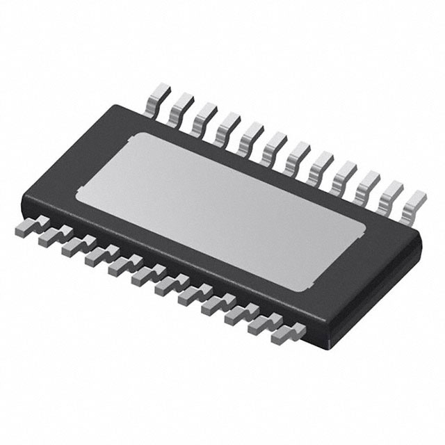


 工商网监
湘ICP备2023018690号
工商网监
湘ICP备2023018690号
