16/32-Bit
Architecture
XC2387E, XC2388E
16/32-Bit Single-Chip Microcontroller
with 32-Bit Performance
XC2000 Family Derivatives / Premium Line
Data Sheet
V1.3 2014-07
Microcontrollers
�Edition 2014-07
Published by
Infineon Technologies AG
81726 Munich, Germany
© 2014 Infineon Technologies AG
All Rights Reserved.
Legal Disclaimer
The information given in this document shall in no event be regarded as a guarantee of conditions or
characteristics. With respect to any examples or hints given herein, any typical values stated herein and/or any
information regarding the application of the device, Infineon Technologies hereby disclaims any and all warranties
and liabilities of any kind, including without limitation, warranties of non-infringement of intellectual property rights
of any third party.
Information
For further information on technology, delivery terms and conditions and prices, please contact the nearest
Infineon Technologies Office (www.infineon.com).
Warnings
Due to technical requirements, components may contain dangerous substances. For information on the types in
question, please contact the nearest Infineon Technologies Office.
Infineon Technologies components may be used in life-support devices or systems only with the express written
approval of Infineon Technologies, if a failure of such components can reasonably be expected to cause the failure
of that life-support device or system or to affect the safety or effectiveness of that device or system. Life support
devices or systems are intended to be implanted in the human body or to support and/or maintain and sustain
and/or protect human life. If they fail, it is reasonable to assume that the health of the user or other persons may
be endangered.
�16/32-Bit
Architecture
XC2387E, XC2388E
16/32-Bit Single-Chip Microcontroller
with 32-Bit Performance
XC2000 Family Derivatives / Premium Line
Data Sheet
V1.3 2014-07
Microcontrollers
�XC2387E, XC2388E
XC2000 Family Derivatives / Premium Line
XC238xE Data Sheet
Revision History: V1.3 2014-07
Previous Versions:
V1.2 2012-06
V1.1 2011-10
V1.0 2010-12
Page
Subjects (major changes since last revision)
9
Added XC2388E-136FxxLR to Basic Device Types
10
Moved XC2388E-136FxxL from Basic to Special Device Types
141
Added package type PG-LQFP-144-23
Trademarks
C166™, TriCore™ and DAVE™ are trademarks of Infineon Technologies AG.
We Listen to Your Comments
Is there any information in this document that you feel is wrong, unclear or missing?
Your feedback will help us to continuously improve the quality of this document.
Please send your proposal (including a reference to this document) to:
mcdocu.comments@infineon.com
Data Sheet
4
V1.3, 2014-07
�XC2387E, XC2388E
XC2000 Family Derivatives / Premium Line
Table of Contents
Table of Contents
1
1.1
1.2
1.3
Summary of Features . . . . . . . . . . . . . . . . . . . . . . . . . . . . . . . . . . . . . . . . 7
Basic Device Types . . . . . . . . . . . . . . . . . . . . . . . . . . . . . . . . . . . . . . . . . . . 9
Special Device Types . . . . . . . . . . . . . . . . . . . . . . . . . . . . . . . . . . . . . . . . 10
Definition of Feature Variants . . . . . . . . . . . . . . . . . . . . . . . . . . . . . . . . . . 11
2
2.1
2.2
General Device Information . . . . . . . . . . . . . . . . . . . . . . . . . . . . . . . . . . 12
Pin Configuration and Definition . . . . . . . . . . . . . . . . . . . . . . . . . . . . . . . . 13
Identification Registers . . . . . . . . . . . . . . . . . . . . . . . . . . . . . . . . . . . . . . . 51
3
3.1
3.2
3.3
3.4
3.5
3.6
3.7
3.8
3.9
3.10
3.11
3.12
3.13
3.14
3.15
3.16
3.17
3.18
3.19
3.20
Functional Description . . . . . . . . . . . . . . . . . . . . . . . . . . . . . . . . . . . . . .
Memory Subsystem and Organization . . . . . . . . . . . . . . . . . . . . . . . . . . . .
External Bus Controller . . . . . . . . . . . . . . . . . . . . . . . . . . . . . . . . . . . . . . .
Central Processing Unit (CPU) . . . . . . . . . . . . . . . . . . . . . . . . . . . . . . . . .
Memory Protection Unit (MPU) . . . . . . . . . . . . . . . . . . . . . . . . . . . . . . . . .
Memory Checker Module (MCHK) . . . . . . . . . . . . . . . . . . . . . . . . . . . . . . .
Interrupt System . . . . . . . . . . . . . . . . . . . . . . . . . . . . . . . . . . . . . . . . . . . .
On-Chip Debug Support (OCDS) . . . . . . . . . . . . . . . . . . . . . . . . . . . . . . .
Capture/Compare Unit (CC2) . . . . . . . . . . . . . . . . . . . . . . . . . . . . . . . . . .
Capture/Compare Units CCU6x . . . . . . . . . . . . . . . . . . . . . . . . . . . . . . . .
General Purpose Timer (GPT12E) Unit . . . . . . . . . . . . . . . . . . . . . . . . . . .
Real Time Clock . . . . . . . . . . . . . . . . . . . . . . . . . . . . . . . . . . . . . . . . . . . .
A/D Converters . . . . . . . . . . . . . . . . . . . . . . . . . . . . . . . . . . . . . . . . . . . . .
Universal Serial Interface Channel Modules (USIC) . . . . . . . . . . . . . . . . .
MultiCAN Module . . . . . . . . . . . . . . . . . . . . . . . . . . . . . . . . . . . . . . . . . . . .
System Timer . . . . . . . . . . . . . . . . . . . . . . . . . . . . . . . . . . . . . . . . . . . . . . .
Watchdog Timer . . . . . . . . . . . . . . . . . . . . . . . . . . . . . . . . . . . . . . . . . . . .
Clock Generation . . . . . . . . . . . . . . . . . . . . . . . . . . . . . . . . . . . . . . . . . . . .
Parallel Ports . . . . . . . . . . . . . . . . . . . . . . . . . . . . . . . . . . . . . . . . . . . . . . .
Power Management . . . . . . . . . . . . . . . . . . . . . . . . . . . . . . . . . . . . . . . . . .
Instruction Set Summary . . . . . . . . . . . . . . . . . . . . . . . . . . . . . . . . . . . . . .
52
52
57
58
60
60
61
62
63
65
67
71
73
74
76
77
77
78
79
80
81
4
4.1
4.1.1
4.1.2
4.1.3
4.1.4
4.1.5
4.2
4.2.1
4.2.2
4.2.3
Electrical Parameters . . . . . . . . . . . . . . . . . . . . . . . . . . . . . . . . . . . . . . .
General Parameters . . . . . . . . . . . . . . . . . . . . . . . . . . . . . . . . . . . . . . . . .
Absolut Maximum Rating Conditions . . . . . . . . . . . . . . . . . . . . . . . . . . .
Operating Conditions . . . . . . . . . . . . . . . . . . . . . . . . . . . . . . . . . . . . . . .
Voltage Range Definition . . . . . . . . . . . . . . . . . . . . . . . . . . . . . . . . . . . .
Pad Timing Definition . . . . . . . . . . . . . . . . . . . . . . . . . . . . . . . . . . . . . . .
Parameter Interpretation . . . . . . . . . . . . . . . . . . . . . . . . . . . . . . . . . . . .
DC Parameters . . . . . . . . . . . . . . . . . . . . . . . . . . . . . . . . . . . . . . . . . . . . .
DC Parameters for Upper Voltage Area . . . . . . . . . . . . . . . . . . . . . . . .
DC Parameters for Lower Voltage Area . . . . . . . . . . . . . . . . . . . . . . . .
Power Consumption . . . . . . . . . . . . . . . . . . . . . . . . . . . . . . . . . . . . . . .
84
84
84
85
87
87
87
88
90
92
94
Data Sheet
5
V1.3, 2014-07
�XC2387E, XC2388E
XC2000 Family Derivatives / Premium Line
Table of Contents
4.3
4.4
4.5
4.6
4.6.1
4.6.2
4.6.2.1
4.6.2.2
4.6.2.3
4.6.3
4.6.4
4.6.5
4.6.5.1
4.6.6
4.6.7
4.6.8
Analog/Digital Converter Parameters . . . . . . . . . . . . . . . . . . . . . . . . . . . . 99
System Parameters . . . . . . . . . . . . . . . . . . . . . . . . . . . . . . . . . . . . . . . . . 104
Flash Memory Parameters . . . . . . . . . . . . . . . . . . . . . . . . . . . . . . . . . . . 107
AC Parameters . . . . . . . . . . . . . . . . . . . . . . . . . . . . . . . . . . . . . . . . . . . . 109
Testing Waveforms . . . . . . . . . . . . . . . . . . . . . . . . . . . . . . . . . . . . . . . 109
Definition of Internal Timing . . . . . . . . . . . . . . . . . . . . . . . . . . . . . . . . . 110
Phase Locked Loop (PLL) . . . . . . . . . . . . . . . . . . . . . . . . . . . . . . . . 111
Wakeup Clock . . . . . . . . . . . . . . . . . . . . . . . . . . . . . . . . . . . . . . . . . 115
Selecting and Changing the Operating Frequency . . . . . . . . . . . . . 115
External Clock Input Parameters . . . . . . . . . . . . . . . . . . . . . . . . . . . . . 116
Pad Properties . . . . . . . . . . . . . . . . . . . . . . . . . . . . . . . . . . . . . . . . . . . 118
External Bus Timing . . . . . . . . . . . . . . . . . . . . . . . . . . . . . . . . . . . . . . . 121
Bus Cycle Control with the READY Input . . . . . . . . . . . . . . . . . . . . 127
Synchronous Serial Interface Timing . . . . . . . . . . . . . . . . . . . . . . . . . . 129
FlexRay Interface Timing . . . . . . . . . . . . . . . . . . . . . . . . . . . . . . . . . . . 133
Debug Interface Timing . . . . . . . . . . . . . . . . . . . . . . . . . . . . . . . . . . . . 135
5
5.1
5.2
5.3
Package and Reliability . . . . . . . . . . . . . . . . . . . . . . . . . . . . . . . . . . . . .
Packaging . . . . . . . . . . . . . . . . . . . . . . . . . . . . . . . . . . . . . . . . . . . . . . . .
Thermal Considerations . . . . . . . . . . . . . . . . . . . . . . . . . . . . . . . . . . . . . .
Quality Declarations . . . . . . . . . . . . . . . . . . . . . . . . . . . . . . . . . . . . . . . . .
Data Sheet
6
141
141
143
144
V1.3, 2014-07
�XC2387E, XC2388E
XC2000 Family Derivatives / Premium Line
Summary of Features
16/32-Bit Single-Chip Microcontroller
with 32-Bit Performance
XC238xE (XC2000 Family)
1
Summary of Features
For a quick overview and easy reference, the features of the XC238xE are summarized
here.
•
•
•
•
•
•
•
High-performance CPU with five-stage pipeline and MPU
– 7.8 ns instruction cycle at 128 MHz CPU clock (single-cycle execution)
– One-cycle 32-bit addition and subtraction with 40-bit result
– One-cycle multiplication (16 × 16 bit)
– Background division (32 / 16 bit) in 21 cycles
– One-cycle multiply-and-accumulate (MAC) instructions
– Enhanced Boolean bit manipulation facilities
– Zero-cycle jump execution
– Additional instructions to support HLL and operating systems
– Register-based design with multiple variable register banks
– Fast context switching support with two additional local register banks
– 16 Kbytes of two-way set-associative Instruction Cache (ICache)
– 16 Mbytes total linear address space for code and data
– 1024 Bytes on-chip special function register area (C166 Family compatible)
– Integrated Memory Protection Unit (MPU)
Interrupt system with 16 priority levels providing 112 interrupt nodes
– Selectable external inputs for interrupt generation and wake-up
– Fastest sample-rate 7.8 ns
Sixteen-channel interrupt-driven single-cycle data transfer with
Peripheral Event Controller (PEC), 24-bit pointers cover total address space
Clock generation from internal or external clock sources,
using on-chip PLL or prescaler
Hardware CRC-Checker with Programmable Polynomial to Supervise On-Chip
Memory Areas
On-chip memory modules
– 8 Kbytes on-chip stand-by RAM (SBRAM)
– 2 Kbytes on-chip dual-port RAM (DPRAM)
– 24 Kbytes on-chip data SRAM (DSRAM)
– Up to 64 Kbytes on-chip program/data SRAM (PSRAM)
– Up to 1 088 Kbytes on-chip program memory (Flash memory)
– Memory content protection through Error Correction Code (ECC)
On-Chip Peripheral Modules
Data Sheet
7
V1.3, 2014-07
�XC2387E, XC2388E
XC2000 Family Derivatives / Premium Line
Summary of Features
–
–
–
–
•
•
•
•
•
•
•
•
•
Multi-functional general purpose timer unit with 5 timers
16-channel general purpose capture/compare unit (CAPCOM2)
Up to four capture/compare units for flexible PWM signal generation (CCU6x)
Two synchronizable 12-bit A/D Converters with up to 24 channels,
conversion time below 1 μs, optional data preprocessing (data reduction, range
check), broken wire detection
– Up to 8 serial interface channels to be used as UART, LIN, high-speed
synchronous channel (SPI), IIC bus interface (10-bit addressing, 400 kbit/s), IIS
interface
– On-chip MultiCAN interface (Rev. 2.0B active) with up to 64 message objects
(Full CAN/Basic CAN) on up to 3 CAN nodes and gateway functionality
– FlexRay™ module (E-Ray) according to protocol specification V2.1,
2 nodes (XC2388E)
– On-chip system timer and on-chip real time clock
Up to 12 Mbytes external address space for code and data
– Programmable external bus characteristics for different address ranges
– Multiplexed or demultiplexed external address/data buses
– Selectable address bus width
– 16-bit or 8-bit data bus width
– Five programmable chip-select signals
Single power supply from 3.0 V to 5.5 V
Power reduction and wake-up modes with flexible power management
Programmable watchdog timer and oscillator watchdog
Up to 118 general purpose I/O lines
On-chip bootstrap loaders
Supported by a full range of development tools including C compilers, macroassembler packages, emulators, evaluation boards, HLL debuggers, simulators,
logic analyzer disassemblers, programming boards
On-chip debug support via Device Access Port (DAP) or JTAG interface
144-pin Green LQFP package, 0.5 mm (19.7 mil) pitch
Data Sheet
8
V1.3, 2014-07
�XC2387E, XC2388E
XC2000 Family Derivatives / Premium Line
Summary of Features
Ordering Information
The ordering code for an Infineon microcontroller provides an exact reference to a
specific product. This ordering code identifies:
•
•
•
the function set of the corresponding product type
the temperature range:
– SAF-…: -40°C to 85°C
– SAH-…: -40°C to 110°C
– SAK-…: -40°C to 125°C
the package and the type of delivery.
For ordering codes for the XC238xE please contact your sales representative or local
distributor.
This document describes several derivatives of the XC238xE group:
Basic Device Types are readily available and
Special Device Types are only available on request.
As this document refers to all of these derivatives, some descriptions may not apply to a
specific product, in particular to the special device types.
For simplicity the term XC238xE is used for all derivatives throughout this document.
1.1
Basic Device Types
Basic device types are available and can be ordered through Infineon’s direct and/or
distribution channels.
Table 1
Synopsis of XC238xE Basic Device Types
1)
Derivative
Program PSRAM
Memory DSRAM3)
Capt./Comp. ADC4) Interfaces4)
Modules
Chan.
2)
XC2388E-136FxxLR 1 088
Kbytes
64 Kbytes CC2
16 + 8 3 CAN Nodes
24 Kbytes CCU60/1/2/3
8 Serial Chan.
2 FlexRay Nodes
1) xx is a placeholder for the available speed grade (in MHz).
2) Specific information about the on-chip Flash memory in Table 3.
3) All derivatives additionally provide 8 Kbytes SBRAM and 2 Kbytes DPRAM.
4) Specific information about the available channels in Table 5.
Analog input channels are listed for each Analog/Digital Converter module separately (ADC0 + ADC1).
Data Sheet
9
V1.3, 2014-07
�XC2387E, XC2388E
XC2000 Family Derivatives / Premium Line
Summary of Features
1.2
Special Device Types
Special device types are only available for high-volume applications on request.
Table 2
Synopsis of XC238xE Special Device Types
Derivative1)
Program
Memory2)
XC2387E-72FxxL
576 Kbytes 64 Kbytes CC2
16 + 8 3 CAN Nodes
24 Kbytes CCU60/1/2/3
6 Serial Chan.
PSRAM
DSRAM3)
Capt./Comp. ADC4) Interfaces4)
Modules
Chan.
XC2387E-104FxxL 832 Kbytes 64 Kbytes CC2
16 + 8 3 CAN Nodes
24 Kbytes CCU60/1/2/3
6 Serial Chan.
XC2387E-136FxxL 1 088
Kbytes
XC2388E-72FxxL
64 Kbytes CC2
16 + 8 3 CAN Nodes
24 Kbytes CCU60/1/2/3
6 Serial Chan.
576 Kbytes 64 Kbytes CC2
16 + 8 3 CAN Nodes
24 Kbytes CCU60/1/2/3
8 Serial Chan.
2 FlexRay Nodes
XC2388E-104FxxL 832 Kbytes 64 Kbytes CC2
16 + 8 3 CAN Nodes
24 Kbytes CCU60/1/2/3
8 Serial Chan.
2 FlexRay Nodes
XC2388E-136FxxL 1 088
Kbytes
64 Kbytes CC2
16 + 8 3 CAN Nodes
24 Kbytes CCU60/1/2/3
8 Serial Chan.
2 FlexRay Nodes
1) xx is a placeholder for the available speed grade (in MHz).
2) Specific information about the on-chip Flash memory in Table 3.
3) All derivatives additionally provide 8 Kbytes SBRAM and 2 Kbytes DPRAM.
4) Specific information about the available channels in Table 5.
Analog input channels are listed for each Analog/Digital Converter module separately (ADC0 + ADC1).
Data Sheet
10
V1.3, 2014-07
�XC2387E, XC2388E
XC2000 Family Derivatives / Premium Line
Summary of Features
1.3
Definition of Feature Variants
The XC238xE types are offered with several Flash memory sizes. Table 3 describes the
location of the available memory areas for each Flash memory size.
Table 3
Flash Memory Allocation
Total Flash Size
Flash Area A1)
Flash Area B
Flash Area C
1 088 Kbytes
C0’0000H …
C0’EFFFH
C1’0000H …
D0’FFFFH
n.a.
832 Kbytes
C0’0000H …
C0’EFFFH
C1’0000H …
CB’FFFFH
D0’0000H …
D0’FFFFH
576 Kbytes
C0’0000H …
C0’EFFFH
C1’0000H …
C7’FFFFH
D0’0000H …
D0’FFFFH
1) The uppermost 4-Kbyte sector of the first Flash segment is reserved for internal use (C0’F000H to C0’FFFFH).
Table 4
Flash Memory Module Allocation (in Kbytes)
Total Flash Size
Flash 01)
Flash 1
Flash 2
Flash 3
Flash 4
1 088 Kbytes
256
256
256
256
64
832 Kbytes
256
256
256
---
64
576 Kbytes
256
256
---
---
64
1) The uppermost 4-Kbyte sector of the first Flash segment is reserved for internal use (C0’F000H to C0’FFFFH).
The XC238xE types are offered with different interface options. Table 5 lists the
available channels for each option.
Table 5
Interface Channel Association
Total Number
Available Channels
16 ADC0 channels
CH0 … CH15
8 ADC1 channels
CH0 … CH7 (overlay: CH8 … CH11)
3 CAN nodes
CAN0, CAN1, CAN2
64 message objects
8 serial channels
U0C0, U0C1, U1C0, U1C1, U2C0, U2C1, U3C0, U3C1
6 serial channels
U0C0, U0C1, U1C0, U1C1, U2C0, U2C1
2 FlexRay nodes
FR0, FR1
Data Sheet
11
V1.3, 2014-07
�XC2387E, XC2388E
XC2000 Family Derivatives / Premium Line
General Device Information
2
General Device Information
The XC238xE series (16/32-Bit Single-Chip Microcontroller
with 32-Bit Performance) is a part of the Infineon XC2000 Family of full-feature singlechip CMOS microcontrollers. These devices extend the functionality and performance of
the C166 Family in terms of instructions (MAC unit), peripherals, and speed. They
combine high CPU performance (up to 128 million instructions per second) with
extended peripheral functionality and enhanced IO capabilities. Optimized peripherals
can be adapted flexibly to meet the application requirements. These derivatives utilize
clock generation via PLL and internal or external clock sources. On-chip memory
modules include program Flash, program RAM, and data RAM.
VAREFVAGND VDDIM VDDI1 VDDP VSS
(2)
(1)
(1)
(4)
(9)
(4)
Port 0
8 bit
XTAL1
XTAL2
Port 1
8 bit
ESR0
ESR1
ESR2
Port 2
14 bit
Port 11
6 bit
Port 3
8 bit
Port 10
16 bit
Port 4
8 bit
Port 9
8 bit
Port 6
4 bit
Port 15
8 bit
Port 7
5 bit
Port 5
16 bit
Port 8
6 bit
PORST
TRST DAP/JTAG Debug
2 bit
2 / 4 bit
TESTM
via Port Pins
MC_HE_ LOGSYMB 144
Figure 1
Data Sheet
Logic Symbol
12
V1.3, 2014-07
�XC2387E, XC2388E
XC2000 Family Derivatives / Premium Line
General Device Information
2.1
Pin Configuration and Definition
144
143
142
141
140
139
138
137
136
135
134
133
132
131
130
129
128
127
126
125
124
123
122
121
120
119
118
117
116
115
114
113
112
111
110
109
V DDPB
P8 .5
P8 .6
ESR 0
ESR 2
ESR1
PORST
XTAL1
XTA L2
P1.7
P9 .7
P1 .6
P9 .6
P1 .5
P1 0.15
P1 .4
P1 0.14
V DDI1
P9.5
P9.4
P1 .3
P1 0.13
P9 .3
P1 0.12
P1 .2
P9 .2
P1 0.11
P1 0.10
P1 .1
P1 0.9
P9 .1
P1 0.8
P9 .0
P1 .0
V DDPB
V SS
The pins of the XC238xE are described in detail in Table 6, which includes all alternate
functions. For further explanations please refer to the footnotes at the end of the table.
The following figure summarizes all pins, showing their locations on the four sides of the
package.
1
2
3
4
5
6
7
8
9
10
11
12
13
14
15
16
17
18
19
20
21
22
23
24
25
26
27
28
29
30
31
32
33
34
35
36
LQFP-144
108
107
106
105
104
103
102
101
100
99
98
97
96
95
94
93
92
91
90
89
88
87
86
85
84
83
82
81
80
79
78
77
76
75
74
73
VDDP B
P3.7
P0.7
P10.7
P3.6
P10.6
P0.6
P3.5
P10.5
P3.4
P10.4
P3.3
P0.5
P10.3
P2.10
P3.2
P2.13
VDDI1
P0.4
P10.2
P3.1
P0.3
P10.1
P3.0
P10.0
P0.2
P2.9
P4.7
P2.8
P0.1
P2.7
P4.6
P4.5
P0.0
VDDP B
VSS
P5.4
P5.5
P5 .6
P5 .7
P5.8
P5.9
P5 .1 0
P5 .1 1
P5 .1 2
P5 .1 3
P5 .1 4
P5 .1 5
P2 .1 2
P2 .1 1
P1 1.5
V DDI1
P2.0
P2.1
P1 1.4
P2.2
P1 1.3
P4.0
P2.3
P1 1.2
P4.1
P2.4
P1 1.1
P1 1.0
P2.5
P4.2
P2.6
P4.4
P4.3
V DDPB
V SS
V DDPB
37
38
39
40
41
42
43
44
45
46
47
48
49
50
51
52
53
54
55
56
57
58
59
60
61
62
63
64
65
66
67
68
69
70
71
72
V SS
V DDPB
TESTM
P7.2
P8.4
TRST
P8.3
P7.0
P7.3
P8.2
P7.1
P7.4
P8.1
V DDI1
VDDIM
P6.0
P6.1
P6.2
P6.3
V DDPA
P15.0
P15.1
P15.2
P15.3
P15.4
P15.5
P15.6
P15.7
V ARE F1
V ARE F0
V AGND
P5.0
P5.1
P5.2
P5.3
V DDPB
MC_HE_PIN144
Figure 2
Data Sheet
XC238xE Pin Configuration (top view)
13
V1.3, 2014-07
�XC2387E, XC2388E
XC2000 Family Derivatives / Premium Line
General Device Information
Key to Pin Definitions
•
•
Ctrl.: The output signal for a port pin is selected by bit field PC in the associated
register Px_IOCRy. Output O0 is selected by setting the respective bit field PC to
1x00B, output O1 is selected by 1x01B, etc.
Output signal OH is controlled by hardware.
Type: Indicates the pad type and its power supply domain (A, B, M, 1).
– St: Standard pad
– Sp: Special pad e.g. XTALx
– DP: Double pad - can be used as standard or high speed pad
– In: Input only pad
– PS: Power supply pad
Table 6
Pin Definitions and Functions
Pin
Symbol
Ctrl.
Type Function
3
TESTM
I
In/B
4
P7.2
O0 / I St/B
Bit 2 of Port 7, General Purpose Input/Output
EMUX0
O1
5
Testmode Enable
Enables factory test modes, must be held HIGH for
normal operation (connect to VDDPB).
An internal pull-up device will hold this pin high
when nothing is driving it.
St/B
External Analog MUX Control Output 0 (ADC1)
CCU62_CCP I
OS0A
St/B
CCU62 Position Input 0
TDI_C
IH
St/B
JTAG Test Data Input
If JTAG pos. C is selected during start-up, an
internal pull-up device will hold this pin high when
nothing is driving it.
P8.4
O0 / I St/B
Bit 4 of Port 8, General Purpose Input/Output
CCU60_COU O1
T61
St/B
CCU60 Channel 1 Output
CCU62_CC6
1
O2
St/B
CCU62 Channel 1 Output
TMS_D
IH
St/B
JTAG Test Mode Selection Input
If JTAG pos. D is selected during start-up, an
internal pull-up device will hold this pin high when
nothing is driving it.
CCU62_CC6
1INB
I
St/B
CCU62 Channel 1 Input
Data Sheet
14
V1.3, 2014-07
�XC2387E, XC2388E
XC2000 Family Derivatives / Premium Line
General Device Information
Table 6
Pin Definitions and Functions (cont’d)
Pin
Symbol
Ctrl.
Type Function
6
TRST
I
In/B
7
P8.3
O0 / I St/B
8
Test-System Reset Input
For normal system operation, pin TRST should be
held low. A high level at this pin at the rising edge
of PORST activates the XC238xE’s debug system.
In this case, pin TRST must be driven low once to
reset the debug system.
An internal pull-down device will hold this pin low
when nothing is driving it.
Bit 3 of Port 8, General Purpose Input/Output
CCU60_COU O1
T60
St/B
CCU60 Channel 0 Output
CCU62_CC6
0
O2
St/B
CCU62 Channel 0 Output
TDI_D
IH
St/B
JTAG Test Data Input
If JTAG pos. D is selected during start-up, an
internal pull-up device will hold this pin low when
nothing is driving it.
CCU62_CC6
0INB
I
St/B
CCU62 Channel 0 Input
P7.0
O0 / I St/B
Bit 0 of Port 7, General Purpose Input/Output
T3OUT
O1
St/B
GPT12E Timer T3 Toggle Latch Output
T6OUT
O2
St/B
GPT12E Timer T6 Toggle Latch Output
TDO_A
OH /
IH
St/B
JTAG Test Data Output / DAP1 Input/Output
If DAP pos. 0 or 2 is selected during start-up, an
internal pull-down device will hold this pin low
when nothing is driving it.
ESR2_1
I
St/B
ESR2 Trigger Input 1
Data Sheet
15
V1.3, 2014-07
�XC2387E, XC2388E
XC2000 Family Derivatives / Premium Line
General Device Information
Table 6
Pin Definitions and Functions (cont’d)
Pin
Symbol
Ctrl.
9
P7.3
O0 / I St/B
Bit 3 of Port 7, General Purpose Input/Output
EMUX1
10
11
Type Function
O1
St/B
External Analog MUX Control Output 1 (ADC1)
U0C1_DOUT O2
St/B
USIC0 Channel 1 Shift Data Output
U0C0_DOUT O3
St/B
USIC0 Channel 0 Shift Data Output
CCU62_CCP I
OS1A
St/B
CCU62 Position Input 1
TMS_C
IH
St/B
JTAG Test Mode Selection Input
If JTAG pos. C is selected during start-up, an
internal pull-up device will hold this pin low when
nothing is driving it.
U0C1_DX0F
I
St/B
USIC0 Channel 1 Shift Data Input
P8.2
O0 / I St/B
Bit 2 of Port 8, General Purpose Input/Output
CCU60_CC6
2
O1
St/B
CCU60 Channel 2 Output
TxDC1
O2
St/B
CAN Node 1 Transmit Data Output
U1C1_DOUT O3
St/B
USIC1 Channel 1 Shift Data output
CCU60_CC6
2INB
I
St/B
CCU60 Channel 2 Input
P7.1
O0 / I St/B
Bit 1 of Port 7, General Purpose Input/Output
EXTCLK
O1
St/B
Programmable Clock Signal Output
CCU62_CTR
APA
I
St/B
CCU62 Emergency Trap Input
BRKIN_C
I
St/B
OCDS Break Signal Input
Data Sheet
16
V1.3, 2014-07
�XC2387E, XC2388E
XC2000 Family Derivatives / Premium Line
General Device Information
Table 6
Pin Definitions and Functions (cont’d)
Pin
Symbol
Ctrl.
12
P7.4
O0 / I St/B
Bit 4 of Port 7, General Purpose Input/Output
EMUX2
13
16
Type Function
O1
St/B
External Analog MUX Control Output 2 (ADC1)
U0C1_DOUT O2
St/B
USIC0 Channel 1 Shift Data Output
U0C1_SCLK
OUT
St/B
USIC0 Channel 1 Shift Clock Output
CCU62_CCP I
OS2A
St/B
CCU62 Position Input 2
TCK_C
IH
St/B
DAP0/JTAG Clock Input
If JTAG pos. C is selected during start-up, an
internal pull-up device will hold this pin high when
nothing is driving it.
If DAP pos. 2 is selected during start-up, an
internal pull-down device will hold this pin low
when nothing is driving it.
U0C0_DX0D
I
St/B
USIC0 Channel 0 Shift Data Input
U0C1_DX1E
I
St/B
USIC0 Channel 1 Shift Clock Input
P8.1
O0 / I St/B
Bit 1 of Port 8, General Purpose Input/Output
CCU60_CC6
1
O1
St/B
CCU60 Channel 1 Output
CCU60_CC6
1INB
I
St/B
CCU60 Channel 1 Input
RxDC1F
I
St/B
CAN Node 1 Receive Data Input
P6.0
O0 / I DA/A Bit 0 of Port 6, General Purpose Input/Output
EMUX0
O1
DA/A External Analog MUX Control Output 0 (ADC0)
TxDC2
O2
DA/A CAN Node 2 Transmit Data Output
BRKOUT
O3
DA/A OCDS Break Signal Output
O3
ADCx_REQG I
TyG
DA/A External Request Gate Input for ADC0/1
U1C1_DX0E
DA/A USIC1 Channel 1 Shift Data Input
Data Sheet
I
17
V1.3, 2014-07
�XC2387E, XC2388E
XC2000 Family Derivatives / Premium Line
General Device Information
Table 6
Pin Definitions and Functions (cont’d)
Pin
Symbol
Ctrl.
17
P6.1
O0 / I DA/A Bit 1 of Port 6, General Purpose Input/Output
EMUX1
O1
DA/A External Analog MUX Control Output 1 (ADC0)
T3OUT
O2
DA/A GPT12E Timer T3 Toggle Latch Output
18
19
Type Function
U1C1_DOUT O3
DA/A USIC1 Channel 1 Shift Data Output
ADCx_REQT I
RyE
DA/A External Request Trigger Input for ADC0/1
RxDC2E
I
DA/A CAN Node 2 Receive Data Input
ESR1_6
I
DA/A ESR1 Trigger Input 6
P6.2
O0 / I DA/A Bit 2 of Port 6, General Purpose Input/Output
EMUX2
O1
DA/A External Analog MUX Control Output 2 (ADC0)
T6OUT
O2
DA/A GPT12E Timer T6 Toggle Latch Output
U1C1_SCLK
OUT
O3
DA/A USIC1 Channel 1 Shift Clock Output
U1C1_DX1C
I
DA/A USIC1 Channel 1 Shift Clock Input
P6.3
O0 / I DA/A Bit 3 of Port 6, General Purpose Input/Output
T3OUT
O2
DA/A GPT12E Timer T3 Toggle Latch Output
U1C1_SELO
0
O3
DA/A USIC1 Channel 1 Select/Control 0 Output
U1C1_DX2D
I
DA/A USIC1 Channel 1 Shift Control Input
ADCx_REQT I
RyF
DA/A External Request Trigger Input for ADC0/1
P15.0
I
In/A
Bit 0 of Port 15, General Purpose Input
ADC1_CH0
I
In/A
Analog Input Channel 0 for ADC1
22
P15.1
I
In/A
Bit 1 of Port 15, General Purpose Input
ADC1_CH1
I
In/A
Analog Input Channel 1 for ADC1
23
P15.2
I
In/A
Bit 2 of Port 15, General Purpose Input
ADC1_CH2
I
In/A
Analog Input Channel 2 for ADC1
21
24
T5INA
I
In/A
GPT12E Timer T5 Count/Gate Input
P15.3
I
In/A
Bit 3 of Port 15, General Purpose Input
ADC1_CH3
I
In/A
Analog Input Channel 3 for ADC1
T5EUDA
I
In/A
GPT12E Timer T5 External Up/Down Control
Input
Data Sheet
18
V1.3, 2014-07
�XC2387E, XC2388E
XC2000 Family Derivatives / Premium Line
General Device Information
Table 6
Pin Definitions and Functions (cont’d)
Pin
Symbol
Ctrl.
Type Function
25
P15.4
I
In/A
Bit 4 of Port 15, General Purpose Input
ADC1_CH4
I
In/A
Analog Input Channel 4 for ADC1
T6INA
I
In/A
GPT12E Timer T6 Count/Gate Input
P15.5
I
In/A
Bit 5 of Port 15, General Purpose Input
26
27
28
29
30
31
32
33
34
35
ADC1_CH5
I
In/A
Analog Input Channel 5 for ADC1
T6EUDA
I
In/A
GPT12E Timer T6 External Up/Down Control
Input
P15.6
I
In/A
Bit 6 of Port 15, General Purpose Input
ADC1_CH6
I
In/A
Analog Input Channel 6 for ADC1
P15.7
I
In/A
Bit 7 of Port 15, General Purpose Input
ADC1_CH7
I
In/A
Analog Input Channel 7 for ADC1
VAREF1
VAREF0
VAGND
-
PS/A Reference Voltage for A/D Converter ADC1
-
PS/A Reference Voltage for A/D Converter ADC0
-
PS/A Reference Ground for A/D Converters ADC0/1
P5.0
I
In/A
Bit 0 of Port 5, General Purpose Input
ADC0_CH0
I
In/A
Analog Input Channel 0 for ADC0
P5.1
I
In/A
Bit 1 of Port 5, General Purpose Input
ADC0_CH1
I
In/A
Analog Input Channel 1 for ADC0
P5.2
I
In/A
Bit 2 of Port 5, General Purpose Input
ADC0_CH2
I
In/A
Analog Input Channel 2 for ADC0
TDI_A
I
In/A
JTAG Test Data Input
P5.3
I
In/A
Bit 3 of Port 5, General Purpose Input
ADC0_CH3
I
In/A
Analog Input Channel 3 for ADC0
T3INA
I
In/A
GPT12E Timer T3 Count/Gate Input
Data Sheet
19
V1.3, 2014-07
�XC2387E, XC2388E
XC2000 Family Derivatives / Premium Line
General Device Information
Table 6
Pin Definitions and Functions (cont’d)
Pin
Symbol
Ctrl.
Type Function
39
P5.4
I
In/A
Bit 4 of Port 5, General Purpose Input
ADC0_CH4
I
In/A
Analog Input Channel 4 for ADC0
CCU63_T12
HRB
I
In/A
External Run Control Input for T12 of CCU63
T3EUDA
I
In/A
GPT12E Timer T3 External Up/Down Control
Input
TMS_A
I
In/A
JTAG Test Mode Selection Input
40
41
42
43
44
P5.5
I
In/A
Bit 5 of Port 5, General Purpose Input
ADC0_CH5
I
In/A
Analog Input Channel 5 for ADC0
CCU60_T12
HRB
I
In/A
External Run Control Input for T12 of CCU60
P5.6
I
In/A
Bit 6 of Port 5, General Purpose Input
ADC0_CH6
I
In/A
Analog Input Channel 6 for ADC0
P5.7
I
In/A
Bit 7 of Port 5, General Purpose Input
ADC0_CH7
I
In/A
Analog Input Channel 7 for ADC0
P5.8
I
In/A
Bit 8 of Port 5, General Purpose Input
ADC0_CH8
I
In/A
Analog Input Channel 8 for ADC0
ADC1_CH8
I
In/A
Analog Input Channel 8 for ADC1
CCU6x_T12H I
RC
In/A
External Run Control Input for T12 of
CCU60/1/2/3
CCU6x_T13H I
RC
In/A
External Run Control Input for T13 of
CCU60/1/2/3
U2C0_DX0F
I
In/A
USIC2 Channel 0 Shift Data Input
P5.9
I
In/A
Bit 9 of Port 5, General Purpose Input
ADC0_CH9
I
In/A
Analog Input Channel 9 for ADC0
ADC1_CH9
I
In/A
Analog Input Channel 9 for ADC1
CC2_T7IN
I
In/A
CAPCOM2 Timer T7 Count Input
Data Sheet
20
V1.3, 2014-07
�XC2387E, XC2388E
XC2000 Family Derivatives / Premium Line
General Device Information
Table 6
Pin Definitions and Functions (cont’d)
Pin
Symbol
Ctrl.
Type Function
45
P5.10
I
In/A
Bit 10 of Port 5, General Purpose Input
ADC0_CH10
I
In/A
Analog Input Channel 10 for ADC0
ADC1_CH10
I
In/A
Analog Input Channel 10 for ADC1
BRKIN_A
I
In/A
OCDS Break Signal Input
U2C1_DX0F
I
In/A
USIC2 Channel 1 Shift Data Input
CCU61_T13
HRA
I
In/A
External Run Control Input for T13 of CCU61
46
47
48
P5.11
I
In/A
Bit 11 of Port 5, General Purpose Input
ADC0_CH11
I
In/A
Analog Input Channel 11 for ADC0
ADC1_CH11
I
In/A
Analog Input Channel 11 for ADC1
P5.12
I
In/A
Bit 12 of Port 5, General Purpose Input
ADC0_CH12
I
In/A
Analog Input Channel 12 for ADC0
P5.13
I
In/A
Bit 13 of Port 5, General Purpose Input
ADC0_CH13
I
In/A
Analog Input Channel 13 for ADC0
ERU_0B1
I
St/B
External Request Unit Channel 0 Input B1
CCU63_T13
HRF
I
In/A
External Run Control Input for T13 of CCU63
49
P5.14
I
In/A
Bit 14 of Port 5, General Purpose Input
ADC0_CH14
I
In/A
Analog Input Channel 14 for ADC0
50
P5.15
I
In/A
Bit 15 of Port 5, General Purpose Input
ADC0_CH15
I
In/A
Analog Input Channel 15 for ADC0
RxDC2F
I
In/A
CAN Node 2 Receive Data Input
P2.12
O0 / I St/B
Bit 12 of Port 2, General Purpose Input/Output
U0C0_SELO
4
O1
St/B
USIC0 Channel 0 Select/Control 4 Output
U0C1_SELO
3
O2
St/B
USIC0 Channel 1 Select/Control 3 Output
TXDC2
O3
St/B
CAN Node 2 Transmit Data Output
READY
IH
St/B
External Bus Interface READY Input
51
Data Sheet
21
V1.3, 2014-07
�XC2387E, XC2388E
XC2000 Family Derivatives / Premium Line
General Device Information
Table 6
Pin Definitions and Functions (cont’d)
Pin
Symbol
Ctrl.
52
P2.11
O0 / I St/B
Bit 11 of Port 2, General Purpose Input/Output
U0C0_SELO
2
O1
St/B
USIC0 Channel 0 Select/Control 2 Output
U0C1_SELO
2
O2
St/B
USIC0 Channel 1 Select/Control 2 Output
U3C1_DOUT O3
St/B
USIC3 Channel 1 Shift Data Output
BHE/WRH
OH
St/B
External Bus Interf. High-Byte Control Output
Can operate either as Byte High Enable (BHE) or
as Write strobe for High Byte (WRH).
P11.5
O0 / I St/B
Bit 5 of Port 11, General Purpose Input/Output
CCU61_CC6
0
O1
St/B
CCU61 Channel 0 Output
CCU61_COU O2
T63
St/B
CCU61 Channel 3 Output
U3C1_SELO
1
O3
St/B
USIC3 Channel 1 Select/Control 1 Output
CCU61_CC6
0INB
I
St/B
CCU61 Channel 0 Input
U3C1_DX2B
I
St/B
USIC3 Channel 1 Shift Control Input
P2.0
O0 / I St/B
Bit 0 of Port 2, General Purpose Input/Output
CCU63_CC6
0
O2
St/B
CCU63 Channel 0 Output
AD13
OH /
IH
St/B
External Bus Interface Address/Data Line 13
RxDC0C
I
St/B
CAN Node 0 Receive Data Input
CCU63_CC6
0INB
I
St/B
CCU63 Channel 0 Input
T5INB
I
St/B
GPT12E Timer T5 Count/Gate Input
53
55
Data Sheet
Type Function
22
V1.3, 2014-07
�XC2387E, XC2388E
XC2000 Family Derivatives / Premium Line
General Device Information
Table 6
Pin Definitions and Functions (cont’d)
Pin
Symbol
Ctrl.
56
P2.1
O0 / I St/B
Bit 1 of Port 2, General Purpose Input/Output
TxDC0
O1
St/B
CAN Node 0 Transmit Data Output
CCU63_CC6
1
O2
St/B
CCU63 Channel 1 Output
AD14
OH /
IH
St/B
External Bus Interface Address/Data Line 14
CCU63_CC6
1INB
I
St/B
CCU63 Channel 1 Input
T5EUDB
I
St/B
GPT12E Timer T5 External Up/Down Control
Input
ESR1_5
I
St/B
ESR1 Trigger Input 5
ERU_0A0
I
St/B
External Request Unit Channel 0 Input A0
P11.4
O0 / I St/B
Bit 4 of Port 11, General Purpose Input/Output
CCU61_CC6
2
O1
St/B
CCU61 Channel 2 Output
U3C1_DOUT O2
St/B
USIC3 Channel 1 Shift Data Output
CCU61_CC6
2INB
I
St/B
CCU61 Channel 2 Input
U3C1_DX0B
I
St/B
USIC3 Channel 1 Shift Data Input
57
58
Type Function
P2.2
O0 / I St/B
Bit 2 of Port 2, General Purpose Input/Output
TxDC1
O1
St/B
CAN Node 1 Transmit Data Output
CCU63_CC6
2
O2
St/B
CCU63 Channel 2 Output
AD15
OH /
IH
St/B
External Bus Interface Address/Data Line 15
CCU63_CC6
2INB
I
St/B
CCU63 Channel 2 Input
ESR2_5
I
St/B
ESR2 Trigger Input 5
ERU_1A0
I
St/B
External Request Unit Channel 1 Input A0
Data Sheet
23
V1.3, 2014-07
�XC2387E, XC2388E
XC2000 Family Derivatives / Premium Line
General Device Information
Table 6
Pin Definitions and Functions (cont’d)
Pin
Symbol
Ctrl.
59
P11.3
O0 / I St/B
60
61
62
Type Function
Bit 3 of Port 11, General Purpose Input/Output
CCU61_COU O1
T63
St/B
CCU61 Channel 3 Output
CCU61_COU O2
T62
St/B
CCU61 Channel 2 Output
CCU61_T13
HRF
I
St/B
External Run Control Input for T13 of CCU61
P4.0
O0 / I St/B
Bit 0 of Port 4, General Purpose Input/Output
CC2_CC24
O3 / I St/B
CAPCOM2 CC24IO Capture Inp./ Compare Out.
CS0
OH
External Bus Interface Chip Select 0 Output
P2.3
O0 / I St/B
St/B
Bit 3 of Port 2, General Purpose Input/Output
U0C0_DOUT O1
St/B
USIC0 Channel 0 Shift Data Output
CCU63_COU O2
T63
St/B
CCU63 Channel 3 Output
CC2_CC16
O3 / I St/B
CAPCOM2 CC16IO Capture Inp./ Compare Out.
A16
OH
St/B
External Bus Interface Address Line 16
ESR2_0
I
St/B
ESR2 Trigger Input 0
U0C0_DX0E
I
St/B
USIC0 Channel 0 Shift Data Input
U0C1_DX0D
I
St/B
USIC0 Channel 1 Shift Data Input
RxDC0A
I
St/B
CAN Node 0 Receive Data Input
P11.2
O0 / I St/B
Bit 2 of Port 11, General Purpose Input/Output
CCU61_CC6
1
O1
St/B
CCU61 Channel 1 Output
U3C1_DOUT O2
St/B
USIC3 Channel 1 Shift Data Output
CCU63_CCP I
OS2A
St/B
CCU63 Position Input 2
CCU61_CC6
1INB
St/B
CCU61 Channel 1 Input
Data Sheet
I
24
V1.3, 2014-07
�XC2387E, XC2388E
XC2000 Family Derivatives / Premium Line
General Device Information
Table 6
Pin Definitions and Functions (cont’d)
Pin
Symbol
Ctrl.
63
P4.1
O0 / I St/B
Bit 1 of Port 4, General Purpose Input/Output
U3C0_SELO
3
O1
St/B
USIC3 Channel Select/Control 3 Output
TxDC2
O2
St/B
CAN Node 2 Transmit Data Output
CC2_CC25
O3 / I St/B
CAPCOM2 CC25IO Capture Inp./ Compare Out.
CS1
OH
St/B
External Bus Interface Chip Select 1 Output
CCU62_CCP I
OS0B
St/B
CCU62 Position Input 0
T4EUDB
I
St/B
GPT12E Timer T4 External Up/Down Control
Input
ESR1_8
I
St/B
ESR1 Trigger Input 8
P2.4
O0 / I St/B
64
65
Type Function
Bit 4 of Port 2, General Purpose Input/Output
U0C1_DOUT O1
St/B
USIC0 Channel 1 Shift Data Output
TxDC0
O2
St/B
CAN Node 0 Transmit Data Output
CC2_CC17
O3 / I St/B
CAPCOM2 CC17IO Capture Inp./ Compare Out.
A17
OH
St/B
External Bus Interface Address Line 17
ESR1_0
I
St/B
ESR1 Trigger Input 0
U0C0_DX0F
I
St/B
USIC0 Channel 0 Shift Data Input
RxDC1A
I
St/B
CAN Node 1 Receive Data Input
P11.1
O0 / I St/B
Bit 1 of Port 11, General Purpose Input/Output
CCU61_COU O1
T61
St/B
CCU61 Channel 1 Output
TxDC0
O2
St/B
CAN Node 0 Transmit Data Output
U3C1_SELO
0
O3
St/B
USIC3 Channel 1 Select/Control 0 Output
CCU63_CCP I
OS1A
St/B
CCU63 Position Input 1
CCU61_CTR
APD
I
St/B
CCU61 Emergency Trap Input
U3C1_DX2A
I
St/B
USIC3 Channel 1 Shift Control Input
Data Sheet
25
V1.3, 2014-07
�XC2387E, XC2388E
XC2000 Family Derivatives / Premium Line
General Device Information
Table 6
Pin Definitions and Functions (cont’d)
Pin
Symbol
Ctrl.
66
P11.0
O0 / I St/B
67
68
Type Function
Bit 0 of Port 11, General Purpose Input/Output
CCU61_COU O1
T60
St/B
CCU61 Channel 0 Output
U3C1_SCLK
OUT
St/B
USIC3 Channel 1 Shift Clock Output
CCU63_CCP I
OS0A
St/B
CCU63 Position Input 0
RxDC0F
St/B
CAN Node 0 Receive Data Input
O2
I
U3C1_DX1A
I
St/B
USIC3 Channel 1 Shift Clock Input
ESR1_7
I
St/B
ESR1 Trigger Input 7
P2.5
O0 / I St/B
Bit 5 of Port 2, General Purpose Input/Output
U0C0_SCLK
OUT
O1
St/B
USIC0 Channel 0 Shift Clock Output
TxDC0
O2
St/B
CAN Node 0 Transmit Data Output
CC2_CC18
O3 / I St/B
CAPCOM2 CC18IO Capture Inp./ Compare Out.
A18
OH
St/B
External Bus Interface Address Line 18
U0C0_DX1D
I
St/B
USIC0 Channel 0 Shift Clock Input
ESR1_10
I
St/B
ESR1 Trigger Input 10
U3C1_DX0D
I
St/B
USIC3 Channel 1 Shift Data Input
P4.2
O0 / I St/B
Bit 2 of Port 4, General Purpose Input/Output
U3C0_SCLK
OUT
O1
St/B
USIC3 Channel 0 Shift Clock Output
TxDC2
O2
St/B
CAN Node 2 Transmit Data Output
CC2_CC26
O3 / I St/B
CAPCOM2 CC26IO Capture Inp./ Compare Out.
CS2
OH
St/B
External Bus Interface Chip Select 2 Output
T2INA
I
St/B
GPT12E Timer T2 Count/Gate Input
CCU62_CCP I
OS1B
St/B
CCU62 Position Input 1
U3C0_DX1B
St/B
USIC3 Channel 0 Shift Clock Input
Data Sheet
I
26
V1.3, 2014-07
�XC2387E, XC2388E
XC2000 Family Derivatives / Premium Line
General Device Information
Table 6
Pin Definitions and Functions (cont’d)
Pin
Symbol
Ctrl.
69
P2.6
O0 / I St/B
Bit 6 of Port 2, General Purpose Input/Output
U0C0_SELO
0
O1
St/B
USIC0 Channel 0 Select/Control 0 Output
U0C1_SELO
1
O2
St/B
USIC0 Channel 1 Select/Control 1 Output
CC2_CC19
O3 / I St/B
CAPCOM2 CC19IO Capture Inp./ Compare Out.
A19
OH
St/B
External Bus Interface Address Line 19
70
71
Type Function
U0C0_DX2D
I
St/B
USIC0 Channel 0 Shift Control Input
RxDC0D
I
St/B
CAN Node 0 Receive Data Input
ESR2_6
I
St/B
ESR2 Trigger Input 6
P4.4
O0 / I St/B
Bit 4 of Port 4, General Purpose Input/Output
U3C0_SELO
2
O1
USIC3 Channel 0 Select/Control 2 Output
CC2_CC28
O3 / I St/B
CAPCOM2 CC28IO Capture Inp./ Compare Out.
CS4
OH
St/B
External Bus Interface Chip Select 4 Output
CLKIN2
I
St/B
Clock Signal Input 2
U3C0_DX2C
I
St/B
USIC3 Channel 0 Shift Control Input
P4.3
O0 / I St/B
U0C1_DOUT O1
St/B
St/B
Bit 3 of Port 4, General Purpose Input/Output
USIC0 Channel 1 Shift Data Output
CC2_CC27
O3 / I St/B
CAPCOM2 CC27IO Capture Inp./ Compare Out.
CS3
OH
St/B
External Bus Interface Chip Select 3 Output
RxDC2A
I
St/B
CAN Node 2 Receive Data Input
T2EUDA
I
St/B
GPT12E Timer T2 External Up/Down Control
Input
CCU62_CCP I
OS2B
St/B
CCU62 Position Input 2
Data Sheet
27
V1.3, 2014-07
�XC2387E, XC2388E
XC2000 Family Derivatives / Premium Line
General Device Information
Table 6
Pin Definitions and Functions (cont’d)
Pin
Symbol
Ctrl.
75
P0.0
O0 / I St/B
76
St/B
USIC1 Channel 0 Shift Data Output
CCU61_CC6
0
O3
St/B
CCU61 Channel 0 IOutput
A0
OH
St/B
External Bus Interface Address Line 0
U1C0_DX0A
I
St/B
USIC1 Channel 0 Shift Data Input
CCU61_CC6
0INA
I
St/B
CCU61 Channel 0 Input
ESR1_11
I
St/B
ESR1 Trigger Input 11
P4.5
O0 / I St/B
CC2_CC29
St/B
O3 / I St/B
Bit 5 of Port 4, General Purpose Input/Output
USIC3 Channel 0 Shift Data Output
CAPCOM2 CC29IO Capture Inp./Compare Out.
CCU61_CCP I
OS0A
St/B
CCU61 Position Input 0
U3C0_DX0B
I
St/B
USIC3 Channel 0 Shift Data Input
ESR2_10
I
St/B
ESR2 Trigger Input 10
P4.6
O0 / I St/B
U3C0_DOUT O1
78
Bit 0 of Port 0, General Purpose Input/Output
U1C0_DOUT O1
U3C0_DOUT O1
77
Type Function
St/B
Bit 6 of Port 4, General Purpose Input/Output
USIC3 Channel 0 Shift Data Output
CC2_CC30
O3 / I St/B
CAPCOM2 CC30IO Capture Inp./ Compare Out.
T4INA
I
St/B
GPT12E Timer T4 Count/Gate Input
CCU61_CCP I
OS1A
St/B
CCU61 Position Input 1
P2.7
O0 / I St/B
Bit 7 of Port 2, General Purpose Input/Output
U0C1_SELO
0
O1
St/B
USIC0 Channel 1 Select/Control 0 Output
U0C0_SELO
1
O2
St/B
USIC0 Channel 0 Select/Control 1 Output
CC2_CC20
O3 / I St/B
CAPCOM2 CC20IO Capture Inp./ Compare Out.
A20
OH
St/B
External Bus Interface Address Line 20
U0C1_DX2C
I
St/B
USIC0 Channel 1 Shift Control Input
RxDC1C
I
St/B
CAN Node 1 Receive Data Input
ESR2_7
I
St/B
ESR2 Trigger Input 7
Data Sheet
28
V1.3, 2014-07
�XC2387E, XC2388E
XC2000 Family Derivatives / Premium Line
General Device Information
Table 6
Pin Definitions and Functions (cont’d)
Pin
Symbol
Ctrl.
79
P0.1
O0 / I St/B
80
Type Function
Bit 1 of Port 0, General Purpose Input/Output
U1C0_DOUT O1
St/B
USIC1 Channel 0 Shift Data Output
TxDC0
O2
St/B
CAN Node 0 Transmit Data Output
CCU61_CC6
1
O3
St/B
CCU61 Channel 1 Output
A1
OH
St/B
External Bus Interface Address Line 1
U1C0_DX0B
I
St/B
USIC1 Channel 0 Shift Data Input
CCU61_CC6
1INA
I
St/B
CCU61 Channel 1 Input
U1C0_DX1A
I
St/B
USIC1 Channel 0 Shift Clock Input
P2.8
O0 / I DP/B Bit 8 of Port 2, General Purpose Input/Output
U0C1_SCLK
OUT
O1
DP/B USIC0 Channel 1 Shift Clock Output
EXTCLK
O2
DP/B Programmable Clock Signal Output
1)
81
CC2_CC21
O3 / I DP/B CAPCOM2 CC21IO Capture Inp./ Compare Out.
A21
OH
DP/B External Bus Interface Address Line 21
U0C1_DX1D
I
DP/B USIC0 Channel 1 Shift Clock Input
P4.7
O0 / I St/B
Bit 7 of Port 4, General Purpose Input/Output
CC2_CC31
O3 / I St/B
CAPCOM2 CC31IO Capture Inp./ Compare Out.
T4EUDA
I
St/B
GPT12E Timer T4 External Up/Down Control
Input
CCU61_CCP I
OS2A
St/B
CCU61 Position Input 2
Data Sheet
29
V1.3, 2014-07
�XC2387E, XC2388E
XC2000 Family Derivatives / Premium Line
General Device Information
Table 6
Pin Definitions and Functions (cont’d)
Pin
Symbol
Ctrl.
82
P2.9
O0 / I St/B
83
Type Function
Bit 9 of Port 2, General Purpose Input/Output
U0C1_DOUT O1
St/B
USIC0 Channel 1 Shift Data Output
TxDC1
O2
St/B
CAN Node 1 Transmit Data Output
CC2_CC22
O3 / I St/B
CAPCOM2 CC22IO Capture Inp./ Compare Out.
A22
OH
St/B
External Bus Interface Address Line 22
CLKIN1
I
St/B
Clock Signal Input 1
TCK_A
IH
St/B
DAP0/JTAG Clock Input
If JTAG pos. A is selected during start-up, an
internal pull-up device will hold this pin high when
nothing is driving it.
If DAP pos. 0 is selected during start-up, an
internal pull-down device will hold this pin low
when nothing is driving it.
P0.2
O0 / I St/B
Bit 2 of Port 0, General Purpose Input/Output
U1C0_SCLK
OUT
O1
St/B
USIC1 Channel 0 Shift Clock Output
TxDC0
O2
St/B
CAN Node 0 Transmit Data Output
CCU61_CC6
2
O3
St/B
CCU61 Channel 2 Output
A2
OH
St/B
External Bus Interface Address Line 2
U1C0_DX1B
I
St/B
USIC1 Channel 0 Shift Clock Input
CCU61_CC6
2INA
I
St/B
CCU61 Channel 2 Input
Data Sheet
30
V1.3, 2014-07
�XC2387E, XC2388E
XC2000 Family Derivatives / Premium Line
General Device Information
Table 6
Pin Definitions and Functions (cont’d)
Pin
Symbol
Ctrl.
84
P10.0
O0 / I St/B
85
86
Type Function
Bit 0 of Port 10, General Purpose Input/Output
U0C1_DOUT O1
St/B
USIC0 Channel 1 Shift Data Output
CCU60_CC6
0
O2
St/B
CCU60 Channel 0 Output
AD0
OH /
IH
St/B
External Bus Interface Address/Data Line 0
CCU60_CC6
0INA
I
St/B
CCU60 Channel 0 Input
ESR1_2
I
St/B
ESR1 Trigger Input 2
U0C0_DX0A
I
St/B
USIC0 Channel 0 Shift Data Input
U0C1_DX0A
I
St/B
USIC0 Channel 1 Shift Data Input
P3.0
O0 / I St/B
Bit 0 of Port 3, General Purpose Input/Output
U2C0_DOUT O1
St/B
USIC2 Channel 0 Shift Data Output
ESR1_1
I
St/B
ESR1 Trigger Input 1
U2C0_DX0A
I
St/B
USIC2 Channel 0 Shift Data Input
U2C0_DX1A
I
St/B
USIC2 Channel 0 Shift Clock Input
P10.1
O0 / I St/B
Bit 1 of Port 10, General Purpose Input/Output
U0C0_DOUT O1
St/B
USIC0 Channel 0 Shift Data Output
CCU60_CC6
1
O2
St/B
CCU60 Channel 1 Output
AD1
OH /
IH
St/B
External Bus Interface Address/Data Line 1
CCU60_CC6
1INA
I
St/B
CCU60 Channel 1 Input
U0C0_DX1A
I
St/B
USIC0 Channel 0 Shift Clock Input
U0C0_DX0B
I
St/B
USIC0 Channel 0 Shift Data Input
Data Sheet
31
V1.3, 2014-07
�XC2387E, XC2388E
XC2000 Family Derivatives / Premium Line
General Device Information
Table 6
Pin Definitions and Functions (cont’d)
Pin
Symbol
Ctrl.
87
P0.3
O0 / I St/B
Bit 3 of Port 0, General Purpose Input/Output
U1C0_SELO
0
O1
St/B
USIC1 Channel 0 Select/Control 0 Output
U1C1_SELO
1
O2
St/B
USIC1 Channel 1 Select/Control 1 Output
CCU61_COU O3
T60
St/B
CCU61 Channel 0 Output
A3
St/B
External Bus Interface Address Line 3
88
89
OH
Type Function
U1C0_DX2A
I
St/B
USIC1 Channel 0 Shift Control Input
RxDC0B
I
St/B
CAN Node 0 Receive Data Input
P3.1
O0 / I St/B
Bit 1 of Port 3, General Purpose Input/Output
U2C0_DOUT O1
St/B
USIC2 Channel 0 Shift Data Output
U2C0_DX0B
I
St/B
USIC2 Channel 0 Shift Data Input
P10.2
O0 / I St/B
Bit 2 of Port 10, General Purpose Input/Output
U0C0_SCLK
OUT
O1
St/B
USIC0 Channel 0 Shift Clock Output
CCU60_CC6
2
O2
St/B
CCU60 Channel 2 Output
U3C0_SELO
1
O3
St/B
USIC3 Channel 0 Select/Control 1 Output
AD2
OH /
IH
St/B
External Bus Interface Address/Data Line 2
CCU60_CC6
2INA
I
St/B
CCU60 Channel 2 Input
U0C0_DX1B
I
St/B
USIC0 Channel 0 Shift Clock Input
U3C0_DX2B
I
St/B
USIC3 Channel 0 Shift Control Input
Data Sheet
32
V1.3, 2014-07
�XC2387E, XC2388E
XC2000 Family Derivatives / Premium Line
General Device Information
Table 6
Pin Definitions and Functions (cont’d)
Pin
Symbol
Ctrl.
90
P0.4
O0 / I St/B
Bit 4 of Port 0, General Purpose Input/Output
U1C1_SELO
0
O1
St/B
USIC1 Channel 1 Select/Control 0 Output
U1C0_SELO
1
O2
St/B
USIC1 Channel 0 Select/Control 1 Output
CCU61_COU O3
T61
St/B
CCU61 Channel 1 Output
A4
St/B
External Bus Interface Address Line 4
92
93
94
OH
Type Function
U1C1_DX2A
I
St/B
USIC1 Channel 1 Shift Control Input
RxDC1B
I
St/B
CAN Node 1 Receive Data Input
ESR2_8
I
St/B
ESR2 Trigger Input 8
P2.13
O0 / I St/B
Bit 13 of Port 2, General Purpose Input/Output
U2C1_SELO
2
O1
St/B
USIC2 Channel 1 Select/Control 2 Output
RxDC2D
I
St/B
CAN Node 2 Receive Data Input
P3.2
O0 / I St/B
Bit 2 of Port 3, General Purpose Input/Output
U2C0_SCLK
OUT
O1
St/B
USIC2 Channel 0 Shift Clock Output
U2C0_DX1B
I
St/B
USIC2 Channel 0 Shift Clock Input
P2.10
O0 / I St/B
Bit 10 of Port 2, General Purpose Input/Output
U0C1_DOUT O1
St/B
USIC0 Channel 1 Shift Data Output
U0C0_SELO
3
O2
St/B
USIC0 Channel 0 Select/Control 3 Output
CC2_CC23
O3 / I St/B
CAPCOM2 CC23IO Capture Inp./ Compare Out.
A23
OH
St/B
External Bus Interface Address Line 23
U0C1_DX0E
I
St/B
USIC0 Channel 1 Shift Data Input
CAPINA
I
St/B
GPT12E Register CAPREL Capture Input
U3C1_DX0A
I
St/B
USIC3 Channel 1 Shift Data Input
Data Sheet
33
V1.3, 2014-07
�XC2387E, XC2388E
XC2000 Family Derivatives / Premium Line
General Device Information
Table 6
Pin Definitions and Functions (cont’d)
Pin
Symbol
Ctrl.
95
P10.3
O0 / I St/B
96
97
Type Function
Bit 3 of Port 10, General Purpose Input/Output
CCU60_COU O2
T60
St/B
CCU60 Channel 0 Output
AD3
OH /
IH
St/B
External Bus Interface Address/Data Line 3
U0C0_DX2A
I
St/B
USIC0 Channel 0 Shift Control Input
U0C1_DX2A
I
St/B
USIC0 Channel 1 Shift Control Input
U3C0_DX0A
I
St/B
USIC3 Channel 0 Shift Data Input
P0.5
O0 / I St/B
Bit 5 of Port 0, General Purpose Input/Output
U1C1_SCLK
OUT
O1
St/B
USIC1 Channel 1 Shift Clock Output
U1C0_SELO
2
O2
St/B
USIC1 Channel 0 Select/Control 2 Output
CCU61_COU O3
T62
St/B
CCU61 Channel 2 Output
A5
OH
St/B
External Bus Interface Address Line 5
U1C1_DX1A
I
St/B
USIC1 Channel 1 Shift Clock Input
U1C0_DX1C
I
St/B
USIC1 Channel 0 Shift Clock Input
P3.3
O0 / I St/B
Bit 3 of Port 3, General Purpose Input/Output
U2C0_SELO
0
O1
St/B
USIC2 Channel 0 Select/Control 0 Output
U2C1_SELO
1
O2
St/B
USIC2 Channel 1 Select/Control 1 Output
U2C0_DX2A
I
St/B
USIC2 Channel 0 Shift Control Input
Data Sheet
34
V1.3, 2014-07
�XC2387E, XC2388E
XC2000 Family Derivatives / Premium Line
General Device Information
Table 6
Pin Definitions and Functions (cont’d)
Pin
Symbol
Ctrl.
98
P10.4
O0 / I St/B
Bit 4 of Port 10, General Purpose Input/Output
U0C0_SELO
3
O1
St/B
USIC0 Channel 0 Select/Control 3 Output
CCU60_COU O2
T61
St/B
CCU60 Channel 1 Output
U3C0_DOUT O3
St/B
USIC3 Channel 0 Shift Data Output
AD4
OH /
IH
St/B
External Bus Interface Address/Data Line 4
U0C0_DX2B
I
St/B
USIC0 Channel 0 Shift Control Input
U0C1_DX2B
I
St/B
USIC0 Channel 1 Shift Control Input
ESR1_9
I
St/B
ESR1 Trigger Input 9
P3.4
O0 / I St/B
Bit 4 of Port 3, General Purpose Input/Output
U2C1_SELO
0
O1
St/B
USIC2 Channel 1 Select/Control 0 Output
U2C0_SELO
1
O2
St/B
USIC2 Channel 0 Select/Control 1 Output
U0C0_SELO
4
O3
St/B
USIC0 Channel 0 Select/Control 4 Output
U2C1_DX2A
I
St/B
USIC2 Channel 1 Shift Control Input
P10.5
O0 / I St/B
Bit 5 of Port 10, General Purpose Input/Output
U0C1_SCLK
OUT
O1
St/B
USIC0 Channel 1 Shift Clock Output
CCU60_COU O2
T62
St/B
CCU60 Channel 2 Output
U2C0_DOUT O3
St/B
USIC2 Channel 0 Shift Data Output
AD5
OH /
IH
St/B
External Bus Interface Address/Data Line 5
U0C1_DX1B
I
St/B
USIC0 Channel 1 Shift Clock Input
99
100
Data Sheet
Type Function
35
V1.3, 2014-07
�XC2387E, XC2388E
XC2000 Family Derivatives / Premium Line
General Device Information
Table 6
Pin Definitions and Functions (cont’d)
Pin
Symbol
Ctrl.
101
P3.5
O0 / I St/B
Bit 5 of Port 3, General Purpose Input/Output
U2C1_SCLK
OUT
O1
St/B
USIC2 Channel 1 Shift Clock Output
U2C0_SELO
2
O2
St/B
USIC2 Channel 0 Select/Control 2 Output
U0C0_SELO
5
O3
St/B
USIC0 Channel 0 Select/Control 5 Output
U2C1_DX1A
I
St/B
USIC2 Channel 1 Shift Clock Input
P0.6
O0 / I St/B
102
103
Type Function
Bit 6 of Port 0, General Purpose Input/Output
U1C1_DOUT O1
St/B
USIC1 Channel 1 Shift Data Output
TxDC1
O2
St/B
CAN Node 1 Transmit Data Output
CCU61_COU O3
T63
St/B
CCU61 Channel 3 Output
A6
OH
St/B
External Bus Interface Address Line 6
U1C1_DX0A
I
St/B
USIC1 Channel 1 Shift Data Input
CCU61_CTR
APA
I
St/B
CCU61 Emergency Trap Input
U1C1_DX1B
I
St/B
USIC1 Channel 1 Shift Clock Input
P10.6
O0 / I St/B
Bit 6 of Port 10, General Purpose Input/Output
U0C0_DOUT O1
St/B
USIC0 Channel 0 Shift Data Output
U1C0_SELO
0
O3
St/B
USIC1 Channel 0 Select/Control 0 Output
AD6
OH /
IH
St/B
External Bus Interface Address/Data Line 6
U0C0_DX0C
I
St/B
USIC0 Channel 0 Shift Data Input
U1C0_DX2D
I
St/B
USIC1 Channel 0 Shift Control Input
CCU60_CTR
APA
I
St/B
CCU60 Emergency Trap Input
Data Sheet
36
V1.3, 2014-07
�XC2387E, XC2388E
XC2000 Family Derivatives / Premium Line
General Device Information
Table 6
Pin Definitions and Functions (cont’d)
Pin
Symbol
Ctrl.
104
P3.6
O0 / I St/B
105
106
107
Type Function
Bit 6 of Port 3, General Purpose Input/Output
U2C1_DOUT O1
St/B
USIC2 Channel 1 Shift Data Output
U0C0_SELO
6
O3
St/B
USIC0 Channel 0 Select/Control 6 Output
U2C1_DX0A
I
St/B
USIC2 Channel 1 Shift Data Input
U2C1_DX1B
I
St/B
USIC2 Channel 1 Shift Clock Input
P10.7
O0 / I St/B
Bit 7 of Port 10, General Purpose Input/Output
U0C1_DOUT O1
St/B
USIC0 Channel 1 Shift Data Output
CCU60_COU O2
T63
St/B
CCU60 Channel 3 Output
AD7
OH /
IH
St/B
External Bus Interface Address/Data Line 7
U0C1_DX0B
I
St/B
USIC0 Channel 1 Shift Data Input
CCU60_CCP I
OS0A
St/B
CCU60 Position Input 0
T4INB
I
St/B
GPT12E Timer T4 Count/Gate Input
P0.7
O0 / I St/B
Bit 7 of Port 0, General Purpose Input/Output
U1C1_DOUT O1
St/B
USIC1 Channel 1 Shift Data Output
U1C0_SELO
3
O2
St/B
USIC1 Channel 0 Select/Control 3 Output
A7
OH
St/B
External Bus Interface Address Line 7
U1C1_DX0B
I
St/B
USIC1 Channel 1 Shift Data Input
CCU61_CTR
APB
I
St/B
CCU61 Emergency Trap Input
P3.7
O0 / I St/B
Bit 7 of Port 3, General Purpose Input/Output
U2C1_DOUT O1
St/B
USIC2 Channel 1 Shift Data Output
U2C0_SELO
3
O2
St/B
USIC2 Channel 0 Select/Control 3 Output
U0C0_SELO
7
O3
St/B
USIC0 Channel 0 Select/Control 7 Output
U2C1_DX0B
I
St/B
USIC2 Channel 1 Shift Data Input
Data Sheet
37
V1.3, 2014-07
�XC2387E, XC2388E
XC2000 Family Derivatives / Premium Line
General Device Information
Table 6
Pin Definitions and Functions (cont’d)
Pin
Symbol
Ctrl.
111
P1.0
O0 / I St/B
Bit 0 of Port 1, General Purpose Input/Output
U1C0_MCLK
OUT
O1
St/B
USIC1 Channel 0 Master Clock Output
U1C0_SELO
4
O2
St/B
USIC1 Channel 0 Select/Control 4 Output
A8
OH
St/B
External Bus Interface Address Line 8
ESR1_3
I
St/B
ESR1 Trigger Input 3
112
Type Function
ERU_0B0
I
St/B
External Request Unit Channel 0 Input B0
CCU62_CTR
APB
I
St/B
CCU62 Emergency Trap Input
T6INB
I
St/B
GPT12E Timer T6 Count/Gate Input
P9.0
O0 / I St/B
Bit 0 of Port 9, General Purpose Input/Output
CCU63_CC6
0
O1
St/B
CCU63 Channel 0 Output
CCU63_CC6
0INA
I
St/B
CCU63 Channel 0 Input
T6EUDB
I
St/B
GPT12E Timer T6 External Up/Down Control
Input
Data Sheet
38
V1.3, 2014-07
�XC2387E, XC2388E
XC2000 Family Derivatives / Premium Line
General Device Information
Table 6
Pin Definitions and Functions (cont’d)
Pin
Symbol
Ctrl.
113
P10.8
O0 / I St/B
Bit 8 of Port 10, General Purpose Input/Output
U0C0_MCLK
OUT
O1
St/B
USIC0 Channel 0 Master Clock Output
U0C1_SELO
0
O2
St/B
USIC0 Channel 1 Select/Control 0 Output
U2C1_DOUT O3
St/B
USIC2 Channel 1 Shift Data Output
AD8
St/B
External Bus Interface Address/Data Line 8
CCU60_CCP I
OS1A
St/B
CCU60 Position Input 1
U0C0_DX1C
St/B
USIC0 Channel 0 Shift Clock Input
114
OH /
IH
I
Type Function
BRKIN_B
I
St/B
OCDS Break Signal Input
T3EUDB
I
St/B
GPT12E Timer T3 External Up/Down Control
Input
ERAY_RxDA
I
St/B
ERAY Receive Data Input Channel A
ESR2_11
I
St/B
ESR2 Trigger Input 11
P9.1
O0 / I DP/B Bit 1 of Port 9, General Purpose Input/Output
CCU63_CC6
1
O1
DP/B CCU63 Channel 1 Output
ERAY_TxDB
O3
DP/B ERAY Transmit Data Output Channel B
CCU63_CC6
1INA
I
DP/B CCU63 Channel 1 Input
Data Sheet
39
V1.3, 2014-07
�XC2387E, XC2388E
XC2000 Family Derivatives / Premium Line
General Device Information
Table 6
Pin Definitions and Functions (cont’d)
Pin
Symbol
Ctrl.
115
P10.9
O0 / I DP/B Bit 9 of Port 10, General Purpose Input/Output
U0C0_SELO
4
O1
DP/B USIC0 Channel 0 Select/Control 4 Output
U0C1_MCLK
OUT
O2
DP/B USIC0 Channel 1 Master Clock Output
116
Type Function
ERAY_TxDA
O3
DP/B ERAY Transmit Data Output Channel A
AD9
OH /
IH
DP/B External Bus Interface Address/Data Line 9
CCU60_CCP I
OS2A
DP/B CCU60 Position Input 2
TCK_B
IH
DP/B DAP0/JTAG Clock Input
If JTAG pos. B is selected during start-up, an
internal pull-up device will hold this pin high when
nothing is driving it.
If DAP pos. 1 is selected during start-up, an
internal pull-down device will hold this pin low
when nothing is driving it.
T3INB
I
DP/B GPT12E Timer T3 Count/Gate Input
P1.1
O0 / I St/B
Bit 1 of Port 1, General Purpose Input/Output
CCU62_COU O1
T62
St/B
CCU62 Channel 2 Output
U1C0_SELO
5
O2
St/B
USIC1 Channel 0 Select/Control 5 Output
U2C1_DOUT O3
St/B
USIC2 Channel 1 Shift Data Output
A9
OH
St/B
External Bus Interface Address Line 9
ESR2_3
I
St/B
ESR2 Trigger Input 3
ERU_1B0
I
St/B
External Request Unit Channel 1 Input B0
U2C1_DX0C
I
St/B
USIC2 Channel 1 Shift Data Input
Data Sheet
40
V1.3, 2014-07
�XC2387E, XC2388E
XC2000 Family Derivatives / Premium Line
General Device Information
Table 6
Pin Definitions and Functions (cont’d)
Pin
Symbol
Ctrl.
117
P10.10
O0 / I St/B
Bit 10 of Port 10, General Purpose Input/Output
U0C0_SELO
0
O1
St/B
USIC0 Channel 0 Select/Control 0 Output
CCU60_COU O2
T63
St/B
CCU60 Channel 3 Output
ERAY_TxEN
A
O3
St/B
ERAY Transmit Enable Output Channel A
AD10
OH /
IH
St/B
External Bus Interface Address/Data Line 10
U0C0_DX2C
I
St/B
USIC0 Channel 0 Shift Control Input
U0C1_DX1A
I
St/B
USIC0 Channel 1 Shift Clock Input
TDI_B
IH
St/B
JTAG Test Data Input
If JTAG pos. B is selected during start-up, an
internal pull-up device will hold this pin high when
nothing is driving it.
P10.11
O0 / I St/B
Bit 11 of Port 10, General Purpose Input/Output
U1C0_SCLK
OUT
O1
St/B
USIC1 Channel 0 Shift Clock Output
BRKOUT
O2
St/B
OCDS Break Signal Output
U3C0_SELO
0
O3
St/B
USIC3 Channel 0 Select/Control 0 Output
AD11
OH /
IH
St/B
External Bus Interface Address/Data Line 11
U1C0_DX1D
I
St/B
USIC1 Channel 0 Shift Clock Input
RxDC2B
I
St/B
CAN Node 2 Receive Data Input
TMS_B
IH
St/B
JTAG Test Mode Selection Input
If JTAG pos. B is selected during start-up, an
internal pull-up device will hold this pin high when
nothing is driving it.
U3C0_DX2A
I
St/B
USIC3 Channel 0 Shift Control Input
118
Data Sheet
Type Function
41
V1.3, 2014-07
�XC2387E, XC2388E
XC2000 Family Derivatives / Premium Line
General Device Information
Table 6
Pin Definitions and Functions (cont’d)
Pin
Symbol
Ctrl.
119
P9.2
O0 / I St/B
Bit 2 of Port 9, General Purpose Input/Output
CCU63_CC6
2
O1
St/B
CCU63 Channel 2 Output
ERAY_TxEN
B
O3
St/B
ERAY Transmit Enable Output Channel B
CCU63_CC6
2INA
I
St/B
CCU63 Channel 2 Input
CAPINB
I
St/B
GPT12E Register CAPREL Capture Input
120
Type Function
P1.2
O0 / I St/B
Bit 2 of Port 1, General Purpose Input/Output
CCU62_CC6
2
O1
St/B
CCU62 Channel 2 Output
U1C0_SELO
6
O2
St/B
USIC1 Channel 0 Select/Control 6 Output
U2C1_SCLK
OUT
O3
St/B
USIC2 Channel 1 Shift Clock Output
A10
OH
St/B
External Bus Interface Address Line 10
ESR1_4
I
St/B
ESR1 Trigger Input 4
ERU_2A0
I
St/B
External Request Unit Channel 2 Input A0
CCU61_T12
HRB
I
St/B
External Run Control Input for T12 of CCU61
CCU62_CC6
2INA
I
St/B
CCU62 Channel 2 Input
U2C1_DX0D
I
St/B
USIC2 Channel 1 Shift Data Input
U2C1_DX1C
I
St/B
USIC2 Channel 1 Shift Clock Input
Data Sheet
42
V1.3, 2014-07
�XC2387E, XC2388E
XC2000 Family Derivatives / Premium Line
General Device Information
Table 6
Pin Definitions and Functions (cont’d)
Pin
Symbol
Ctrl.
121
P10.12
O0 / I St/B
122
123
Type Function
Bit 12 of Port 10, General Purpose Input/Output
U1C0_DOUT O1
St/B
USIC1 Channel 0 Shift Data Output
TxDC2
O2
St/B
CAN Node 2 Transmit Data Output
TDO_B
OH /
IH
St/B
JTAG Test Data Output / DAP1 Input/Output
If DAP pos. 1 is selected during start-up, an
internal pull-down device will hold this pin low
when nothing is driving it.
AD12
OH /
IH
St/B
External Bus Interface Address/Data Line 12
U1C0_DX0C
I
St/B
USIC1 Channel 0 Shift Data Input
U1C0_DX1E
I
St/B
USIC1 Channel 0 Shift Clock Input
P9.3
O0 / I St/B
Bit 3 of Port 9, General Purpose Input/Output
CCU63_COU O1
T60
St/B
CCU63 Channel 0 Output
BRKOUT
O2
St/B
OCDS Break Signal Output
P10.13
O0 / I St/B
Bit 13 of Port 10, General Purpose Input/Output
U1C0_DOUT O1
St/B
USIC1 Channel 0 Shift Data Output
U1C0_SELO
3
O3
St/B
USIC1 Channel 0 Select/Control 3 Output
WR/WRL
OH
St/B
External Bus Interface Write Strobe Output
Active for each external write access, when WR,
active for ext. writes to the low byte, when WRL.
U1C0_DX0D
I
St/B
USIC1 Channel 0 Shift Data Input
Data Sheet
43
V1.3, 2014-07
�XC2387E, XC2388E
XC2000 Family Derivatives / Premium Line
General Device Information
Table 6
Pin Definitions and Functions (cont’d)
Pin
Symbol
Ctrl.
124
P1.3
O0 / I St/B
125
126
Type Function
Bit 3 of Port 1, General Purpose Input/Output
CCU62_COU O1
T63
St/B
CCU62 Channel 3 Output
U1C0_SELO
7
O2
St/B
USIC1 Channel 0 Select/Control 7 Output
U2C0_SELO
4
O3
St/B
USIC2 Channel 0 Select/Control 4 Output
A11
OH
St/B
External Bus Interface Address Line 11
ESR2_4
I
St/B
ESR2 Trigger Input 4
ERU_3A0
I
St/B
External Request Unit Channel 3 Input A0
CCU62_T12
HRB
I
St/B
External Run Control Input for T12 of CCU62
P9.4
O0 / I St/B
Bit 4 of Port 9, General Purpose Input/Output
CCU63_COU O1
T61
St/B
CCU63 Channel 1 Output
U2C0_DOUT O2
St/B
USIC2 Channel 0 Shift Data Output
CCU62_COU O3
T63
St/B
CCU62 Channel 3 Output
P9.5
O0 / I St/B
Bit 5 of Port 9, General Purpose Input/Output
CCU63_COU O1
T62
St/B
CCU63 Channel 2 Output
U2C0_DOUT O2
St/B
USIC2 Channel 0 Shift Data Output
CCU62_COU O3
T62
St/B
CCU62 Channel 2 Output
U2C0_DX0E
I
St/B
USIC2 Channel 0 Shift Data Input
CCU60_CCP I
OS2B
St/B
CCU60 Position Input 2
Data Sheet
44
V1.3, 2014-07
�XC2387E, XC2388E
XC2000 Family Derivatives / Premium Line
General Device Information
Table 6
Pin Definitions and Functions (cont’d)
Pin
Symbol
Ctrl.
128
P10.14
O0 / I St/B
Bit 14 of Port 10, General Purpose Input/Output
U1C0_SELO
1
O1
St/B
USIC1 Channel 0 Select/Control 1 Output
U0C1_DOUT O2
St/B
USIC0 Channel 1 Shift Data Output
U3C0_SCLK
OUT
O3
St/B
USIC3 Channel 0 Shift Clock Output
RD
OH
St/B
External Bus Interface Read Strobe Output
ESR2_2
I
St/B
ESR2 Trigger Input 2
U0C1_DX0C
I
St/B
USIC0 Channel 1 Shift Data Input
U3C0_DX1A
I
St/B
USIC3 Channel 0 Shift Clock Input
P1.4
O0 / I St/B
129
130
Type Function
Bit 4 of Port 1, General Purpose Input/Output
CCU62_COU O1
T61
St/B
CCU62 Channel 1 Output
U1C1_SELO
4
O2
St/B
USIC1 Channel 1 Select/Control 4 Output
U2C0_SELO
5
O3
St/B
USIC2 Channel 0 Select/Control 5 Output
A12
OH
St/B
External Bus Interface Address Line 12
U2C0_DX2B
I
St/B
USIC2 Channel 0 Shift Control Input
P10.15
O0 / I St/B
Bit 15 of Port 10, General Purpose Input/Output
U1C0_SELO
2
O1
St/B
USIC1 Channel 0 Select/Control 2 Output
U0C1_DOUT O2
St/B
USIC0 Channel 1 Shift Data Output
U1C0_DOUT O3
St/B
USIC1 Channel 0 Shift Data Output
ALE
OH
St/B
External Bus Interf. Addr. Latch Enable Output
U0C1_DX1C
I
St/B
USIC0 Channel 1 Shift Clock Input
Data Sheet
45
V1.3, 2014-07
�XC2387E, XC2388E
XC2000 Family Derivatives / Premium Line
General Device Information
Table 6
Pin Definitions and Functions (cont’d)
Pin
Symbol
Ctrl.
131
P1.5
O0 / I St/B
132
133
Type Function
Bit 5 of Port 1, General Purpose Input/Output
CCU62_COU O1
T60
St/B
CCU62 Channel 0 Output
U1C1_SELO
3
O2
St/B
USIC1 Channel 1 Select/Control 3 Output
BRKOUT
O3
St/B
OCDS Break Signal Output
A13
OH
St/B
External Bus Interface Address Line 13
U2C0_DX0C
I
St/B
USIC2 Channel 0 Shift Data Input
P9.6
O0 / I St/B
Bit 6 of Port 9, General Purpose Input/Output
CCU63_COU O1
T63
St/B
CCU63 Channel 3 Output
CCU63_COU O2
T62
St/B
CCU63 Channel 2 Output
CCU62_COU O3
T61
St/B
CCU62 Channel 1 Output
CCU63
_CTRAPA
I
St/B
CCU63 Emergency Trap Input
CCU60_CCP I
OS1B
St/B
CCU60 Position Input 1
ERAY_RxDB
I
St/B
ERAY Receive Data Input Channel B
P1.6
O0 / I St/B
Bit 6 of Port 1, General Purpose Input/Output
CCU62_CC6
1
O1 / I St/B
CCU62 Channel 1 Output
U1C1_SELO
2
O2
St/B
USIC1 Channel 1 Select/Control 2 Output
U2C0_DOUT O3
St/B
USIC2 Channel 0 Shift Data Output
A14
OH
St/B
External Bus Interface Address Line 14
U2C0_DX0D
I
St/B
USIC2 Channel 0 Shift Data Input
CCU62_CC6
1INA
I
St/B
CCU62 Channel 1 Input
Data Sheet
46
V1.3, 2014-07
�XC2387E, XC2388E
XC2000 Family Derivatives / Premium Line
General Device Information
Table 6
Pin Definitions and Functions (cont’d)
Pin
Symbol
Ctrl.
134
P9.7
O0 / I St/B
135
Type Function
Bit 7 of Port 9, General Purpose Input/Output
CCU62_COU O1
T60
St/B
CCU62 Channel 0 Output
CCU62_COU O2
T63
St/B
CCU62 Channel 3 Output
CCU63_CTR
APB
I
St/B
CCU63 Emergency Trap Input
U2C0_DX1D
I
St/B
USIC2 Channel 0 Shift Clock Input
CCU60_CCP I
OS0B
St/B
CCU60 Position Input 0
P1.7
O0 / I St/B
Bit 7 of Port 1, General Purpose Input/Output
CCU62_CC6
0
O1
St/B
CCU62 Channel 0 Output
U1C1_MCLK
OUT
O2
St/B
USIC1 Channel 1 Master Clock Output
U2C0_SCLK
OUT
O3
St/B
USIC2 Channel 0 Shift Clock Output
A15
OH
St/B
External Bus Interface Address Line 15
U2C0_DX1C
I
St/B
USIC2 Channel 0 Shift Clock Input
CCU62_CC6
0INA
I
St/B
CCU62 Channel 0 Input
136
XTAL2
O
Sp/M Crystal Oscillator Amplifier Output
137
XTAL1
I
Sp/M Crystal Oscillator Amplifier Input
To clock the device from an external source, drive
XTAL1, while leaving XTAL2 unconnected.
Voltages on XTAL1 must comply to the core
supply voltage VDDIM.
ESR2_9
I
St/B
Data Sheet
ESR2 Trigger Input 9
47
V1.3, 2014-07
�XC2387E, XC2388E
XC2000 Family Derivatives / Premium Line
General Device Information
Table 6
Pin Definitions and Functions (cont’d)
Pin
Symbol
Ctrl.
Type Function
138
PORST
I
In/B
139
ESR1
O0 / I St/B
External Service Request 1
After power-up, an internal weak pull-up device
holds this pin high when nothing is driving it.
RxDC0E
I
St/B
CAN Node 0 Receive Data Input
U1C0_DX0F
I
St/B
USIC1 Channel 0 Shift Data Input
U1C0_DX2C
I
St/B
USIC1 Channel 0 Shift Control Input
U1C1_DX0C
I
St/B
USIC1 Channel 1 Shift Data Input
U1C1_DX2B
I
St/B
USIC1 Channel 1 Shift Control Input
U2C1_DX2C
I
St/B
USIC2 Channel 1 Shift Control Input
ESR2
O0 / I St/B
External Service Request 2
After power-up, an internal weak pull-up device
holds this pin high when nothing is driving it.
RxDC1E
I
St/B
CAN Node 1 Receive Data Input
CCU60_CTR
APC
I
St/B
CCU60 Emergency Trap Input
CCU61_CTR
APC
I
St/B
CCU61 Emergency Trap Input
CCU62_CTR
APC
I
St/B
CCU62 Emergency Trap Input
CCU63_CTR
APC
I
St/B
CCU63 Emergency Trap Input
U1C1_DX0D
I
St/B
USIC1 Channel 1 Shift Data Input
U1C1_DX2C
I
St/B
USIC1 Channel 1 Shift Control Input
U2C1_DX0E
I
St/B
USIC2 Channel 1 Shift Data Input
U2C1_DX2B
I
St/B
USIC2 Channel 1 Shift Control Input
140
Data Sheet
Power On Reset Input
A low level at this pin resets the XC238xE
completely. A spike filter suppresses input pulses
100 ns safely pass the filter.
The minimum duration for a safe recognition
should be 120 ns.
An internal pull-up device will hold this pin high
when nothing is driving it.
48
V1.3, 2014-07
�XC2387E, XC2388E
XC2000 Family Derivatives / Premium Line
General Device Information
Table 6
Pin Definitions and Functions (cont’d)
Pin
Symbol
Ctrl.
141
ESR0
O0 / I St/B
External Service Request 0
After power-up, ESR0 operates as open-drain
bidirectional reset with a weak pull-up.
U1C0_DX0E
I
St/B
USIC1 Channel 0 Shift Data Input
U1C0_DX2B
I
St/B
USIC1 Channel 0 Shift Control Input
P8.6
O0 / I St/B
142
143
Type Function
Bit 6 of Port 8, General Purpose Input/Output
CCU60_COU O1
T63
St/B
CCU60 Channel 3 Output
MCHK_MAT
CH
O3
St/B
Memory Checker Match Output
CCU60_CTR
APB
I
St/B
CCU60 Emergency Trap Input
BRKIN_D
I
St/B
OCDS Break Signal Input
CCU62_CTR
APD
I
St/B
CCU62 Emergency Trap Input
P8.5
O0 / I St/B
Bit 5 of Port 8, General Purpose Input/Output
CCU60_COU O1
T62
St/B
CCU60 Channel 2 Output
CCU62_CC6
2
O2
St/B
CCU62 Channel 2 Output
TCK_D
IH
St/B
DAP0/JTAG Clock Input
If JTAG pos. D is selected during start-up, an
internal pull-up device will hold this pin high when
nothing is driving it.
CCU62_CC6
2INB
I
St/B
CCU62 Channel 2 Input
15
VDDIM
-
PS/M Digital Core Supply Voltage for Domain M
Decouple with a ceramic capacitor, see Data
Sheet for details.
14,
54,
91,
127
VDDI1
-
PS/1 Digital Core Supply Voltage for Domain 1
Decouple with a ceramic capacitor, see Data
Sheet for details.
All VDDI1 pins must be connected to each other.
Data Sheet
49
V1.3, 2014-07
�XC2387E, XC2388E
XC2000 Family Derivatives / Premium Line
General Device Information
Table 6
Pin Definitions and Functions (cont’d)
Pin
Symbol
Ctrl.
Type Function
20
VDDPA
-
PS/A Digital Pad Supply Voltage for Domain A
Connect decoupling capacitors to adjacent
VDDP/VSS pin pairs as close as possible to the pins.
Note: The A/D Converters and ports P5, P6 and
P15 are fed from supply voltage VDDPA.
VDDPB
2,
36,
38,
72,
74,
108,
110,
144
1,
37,
73,
109
VSS
-
PS/B Digital Pad Supply Voltage for Domain B
Connect decoupling capacitors to adjacent
VDDP/VSS pin pairs as close as possible to the pins.
Note: The on-chip voltage regulators and all ports
except P5, P6 and P15 are fed from supply
voltage VDDPB.
-
PS/-- Digital Ground
All VSS pins must be connected to the ground-line
or ground-plane.
Note: Also the exposed pad is connected
internally to VSS. To improve the EMC
behavior, it is recommended to connect the
exposed pad to the board ground.
For thermal aspects, please refer to the
Data Sheet. Board layout examples are
given in an application note.
1) To generate the reference clock output for bus timing measurement, fSYS must be selected as source for
EXTCLK and P2.8 must be selected as output pin. Also the high-speed clock pad must be enabled. This
configuration is referred to as reference clock output signal CLKOUT.
Data Sheet
50
V1.3, 2014-07
�XC2387E, XC2388E
XC2000 Family Derivatives / Premium Line
General Device Information
2.2
Identification Registers
The identification registers describe the current version of the XC238xE and of its
modules.
Table 7
XC238xE Identification Registers
Short Name
Value
Address
SCU_IDMANUF
1820H
00’F07EH
SCU_IDCHIP
4801H
00’F07CH
SCU_IDMEM
310FH
00’F07AH
SCU_IDPROG
1313H
00’F078H
JTAG_ID
101B’F083H
---
Data Sheet
51
Notes
Step AA
V1.3, 2014-07
�XC2387E, XC2388E
XC2000 Family Derivatives / Premium Line
Functional Description
3
Functional Description
The architecture of the XC238xE combines advantages of RISC, CISC, and DSP
processors with an advanced peripheral subsystem in a well-balanced design. On-chip
memory blocks allow the design of compact systems-on-silicon with maximum
performance suited for computing, control, and communication.
The on-chip memory blocks (program code memory and SRAM, dual-port RAM, data
SRAM) and the generic peripherals are connected to the CPU by separate high-speed
buses. Another bus, the LXBus, connects additional on-chip resources and external
resources. This bus structure enhances overall system performance by enabling the
concurrent operation of several subsystems of the XC238xE.
The block diagram gives an overview of the on-chip components and the advanced
internal bus structure of the XC238xE.
3.1
Memory Subsystem and Organization
The memory space of the XC238xE is configured in the von Neumann architecture. In
this architecture all internal and external resources, including code memory, data
memory, registers and I/O ports, are organized in the same linear address space.
Table 8
XC238xE Memory Map 1)
Address Area
Start Loc. End Loc.
Area Size2)
IMB register space
FF’FF00H
FF’FFFFH
256 Bytes
Reserved
F0’0000H
FF’FEFFH
< 1 Mbyte
Minus IMB registers
Reserved for EPSRAM
E9’0000H
EF’FFFFH
448 Kbytes
Mirrors EPSRAM
Emulated PSRAM
E8’0000H
E8’FFFFH
up to
64 Kbytes
With Flash timing
Reserved for PSRAM
E1’0000H
E7’FFFFH
448 Kbytes
Mirrors PSRAM
PSRAM
E0’0000H
E0’FFFFH
up to
64 Kbytes
Program SRAM
Reserved for Flash
D1’0000H
DF’FFFFH
448 Kbytes
Flash 4
D0’0000H
D0’FFFFH
64 Kbytes
Flash 3
CC’0000H CF’FFFFH
256 Kbytes
Flash 2
C8’0000H
CB’FFFFH
256 Kbytes
Flash 1
C4’0000H
C7’FFFFH
256 Kbytes
Flash 0
C0’0000H
C3’FFFFH
256 Kbytes3)
External memory area
40’0000H
BF’FFFFH
8 Mbytes
External IO area4)
21’0000H
3F’FFFFH
1 984 Kbytes
Data Sheet
52
Notes
Minus res. seg.
V1.3, 2014-07
�XC2387E, XC2388E
XC2000 Family Derivatives / Premium Line
Functional Description
Table 8
XC238xE Memory Map (cont’d)1)
Address Area
Start Loc. End Loc.
Area Size2)
Notes
MultiCAN alternate regs. 20’8000H
20’AFFFH
12 Kbytes
Accessed via EBC
FlexRay registers
20’7000H
20’7FFFH
4 Kbytes
Accessed via EBC
Reserved
20’6800H
20’6FFFH
2 Kbytes
MultiCAN registers
20’0000H
20’3FFFH
16 Kbytes
External memory area
01’0000H
1F’FFFFH
1984 Kbytes
SFR area
00’FE00H
00’FFFFH
0.5 Kbytes
Dualport RAM (DPRAM) 00’F600H
00’FDFFH
2 Kbytes
Reserved for DPRAM
00’F200H
00’F5FFH
1 Kbytes
ESFR area
00’F000H
00’F1FFH
0.5 Kbytes
XSFR area
00’E000H
00’EFFFH
4 Kbytes
Data SRAM (DSRAM)
00’8000H
00’DFFFH
24 Kbytes
External memory area
00’0000H
00’7FFFH
32 Kbytes
Accessed via EBC
1) Accesses to the shaded areas are reserved. In devices with external bus interface these accesses generate
external bus accesses.
2) The areas marked with “ VDDP or VIN < VSS) the
voltage on VDDP pins with respect to ground (VSS) must not exceed the values defined by
the absolute maximum ratings.
Table 12
Absolute Maximum Rating Parameters
Parameter
Symbol
Values
Unit
Min.
Typ.
Max.
Note /
Test Condition
Output current on a pin
when high value is driven
IOH SR
-30
−
−
mA
Output current on a pin
when low value is driven
IOL SR
−
−
30
mA
-10
−
10
mA
1)
−
−
100
mA
1)
IOV SR
Absolute sum of overload Σ|IOV|
Overload current
currents
SR
Junction Temperature
TJ SR
-40
TST SR -65
VDDP SR -0.5
−
150
°C
−
150
°C
−
6.0
V
VIN SR
−
VDDP
V
Storage Temperature
Digital supply voltage for
IO pads and voltage
regulators
Voltage on any pin with
respect to ground (Vss)
-0.5
VIN ≤ VDDP(max)
+ 0.5
1) Overload condition occurs if the input voltage VIN is out of the absolute maximum rating range. In this case the
current must be limited to the listed values by design measures.
Data Sheet
84
V1.3, 2014-07
�XC2387E, XC2388E
XC2000 Family Derivatives / Premium Line
Electrical Parameters
4.1.2
Operating Conditions
The following operating conditions must not be exceeded to ensure correct operation of
the XC238xE. All parameters specified in the following sections refer to these operating
conditions, unless otherwise noticed.
Note: Typical parameter values refer to room temperature and nominal supply voltage,
minimum/maximum
parameter
values
also
include
conditions
of
minimum/maximum temperature and minimum/maximum supply voltage.
Additional details are described where applicable.
Table 13
Operating Conditions
Parameter
Symbol
Voltage Regulator Buffer
Capacitance for DMP_M
CEVRM
Voltage Regulator Buffer
Capacitance for DMP_1
CEVR1
External Load
Capacitance
CL SR
Values
Unit
Note /
Test Condition
4.7
μF
1)
−
2.2
μF
1)2)
203)
−
pF
pin out
driver= default
Min.
Typ.
Max.
1.0
−
0.68
−
SR
SR
4)
System frequency
Overload current for
analog inputs6)
fSYS SR −
IOVA SR -2
Overload current for digital IOVD SR -5
inputs6)
Overload current coupling KOVA
factor for analog inputs7)
CC
−
−
Overload current coupling KOVD
CC
factor for digital I/O pins
−
−
Data Sheet
85
−
128
MHz
5)
−
5
mA
not subject to
production test
−
5
mA
not subject to
production test
2.5 x
10-4
1.5 x
10-3
-
IOV < 0 mA;
1.0 x
10-6
1.0 x
10-4
-
1.0 x
10-2
3.0 x
10-2
IOV < 0 mA;
1.0 x
10-4
5.0 x
10-3
IOV > 0 mA;
not subject to
production test
IOV > 0 mA;
not subject to
production test
not subject to
production test
not subject to
production test
V1.3, 2014-07
�XC2387E, XC2388E
XC2000 Family Derivatives / Premium Line
Electrical Parameters
Table 13
Operating Conditions (cont’d)
Parameter
Symbol
Values
Min.
Typ.
Max.
Σ|IOV|
SR
−
−
50
Digital core supply voltage VDDIM
for domain M8)
CC
−
1.5
−
Digital core supply voltage VDDI1
for domain 18)
CC
−
1.5
−
Absolute sum of overload
currents
Unit
Note /
Test Condition
mA
not subject to
production test
Digital supply voltage for
IO pads and voltage
regulators
VDDP SR 3.0
−
5.5
V
Operation
3.1
−
−
V
Power up9)
Digital ground voltage
VSS SR
−
0
−
V
1) To ensure the stability of the voltage regulators the EVRs must be buffered with ceramic capacitors. Separate
buffer capacitors with the recomended values shall be connected as close as possible to each VDDIM and VDDI1
pin to keep the resistance of the board tracks below 2 Ω. Connect all VDDI1 pins together. The minimum
capacitance value is required for proper operation under all conditions (e.g. temperature). Higher values
slightly increase the startup time.
2) Use one Capacitor for each pin.
3) This is the reference load. For bigger capacitive loads, use the derating factors listed in the PAD properties
section.
4) The timing is valid for pin drivers operating in default current mode (selected after reset). Reducing the output
current may lead to increased delays or reduced driving capability (CL).
5) The operating frequency range may be reduced for specific device types. This is indicated in the device
designation (...FxxL). 80 MHz devices are marked ...F80L.
6) Overload conditions occur if the standard operating conditions are exceeded, i.e. the voltage on any pin
exceeds the specified range: VOV > VIHmax (IOV > 0) or VOV < VILmin ((IOV < 0). The absolute sum of input
overload currents on all pins may not exceed 50 mA. The supply voltages must remain within the specified
limits. Proper operation under overload conditions depends on the application. Overload conditions must not
occur on pin XTAL1 (powered by VDDIM).
7) An overload current (IOV) through a pin injects a certain error current (IINJ) into the adjacent pins. This error
current adds to the respective pins leakage current (IOZ). The amount of error current depends on the overload
current and is defined by the overload coupling factor KOV. The polarity of the injected error current is inverse
compared to the polarity of the overload current that produces it.The total current through a pin is |ITOT| = |IOZ|
+ (|IOV| KOV). The additional error current may distort the input voltage on analog inputs.
8) Value is controlled by on-chip regulator
9) To ensure a stable power up sequence, the external supply voltage must reach or exceed a level of 3.1 V
during power up for at least 0.5 ms.
For normal operation the complete specified voltage range is available.
Data Sheet
86
V1.3, 2014-07
�XC2387E, XC2388E
XC2000 Family Derivatives / Premium Line
Electrical Parameters
4.1.3
Voltage Range Definition
The XC238xE timing depends on the supply voltage. If such a dependency exists the
timing values are given for 2 voltage areas commonly used. The voltage areas are
defined in the following tables.
Table 14
Upper Voltage Range Definition
Parameter
Symbol
Values
Min.
Digital supply voltage for
IO pads and voltage
regulators
Table 15
VDDP SR 4.5
4.75
Note /
Test Condition
5.5
V
5.25
V
fSYS ≤ 100 MHz
fSYS ≤ 128 MHz
Max.
5
5
Lower Voltage Range Definition
Parameter
Symbol
Digital supply voltage for
IO pads and voltage
regulators
VDDP SR 3.0
Values
Min.
4.1.4
Unit
Typ.
Unit
Typ.
Max.
3.3
4.5
Note /
Test Condition
V
Pad Timing Definition
If not otherwise noted, all timing parameters are tested and are valid for the
corresponding output pins operating in strong driver, fast edge mode.
See also “Pad Properties” on Page 118.
4.1.5
Parameter Interpretation
The parameters listed in the following include both the characteristics of the XC238xE
and its demands on the system. To aid in correctly interpreting the parameters when
evaluating them for a design, they are marked accordingly in the column “Symbol”:
CC (Controller Characteristics):
The logic of the XC238xE provides signals with the specified characteristics.
SR (System Requirement):
The external system must provide signals with the specified characteristics to the
XC238xE.
Data Sheet
87
V1.3, 2014-07
�XC2387E, XC2388E
XC2000 Family Derivatives / Premium Line
Electrical Parameters
4.2
DC Parameters
These parameters are static or average values that may be exceeded during switching
transitions (e.g. output current).
Leakage current is strongly dependent on the operating temperature and the voltage
level at the respective pin. The maximum values in the following tables apply under worst
case conditions, i.e. maximum temperature and an input level equal to the supply
voltage.
The value for the leakage current in an application can be determined by using the
respective leakage derating formula (see tables) with values from that application.
The pads of the XC238xE are designed to operate in various driver modes. The DC
parameter specifications refer to the pad current limits specified in Section 4.6.4.
Supply Voltage Restrictions
The XC238xE can operate within a wide supply voltage range from 3.0 V to 5.5 V.
However, during operation this supply voltage must remain within 10 percent of the
selected nominal supply voltage. It cannot vary across the full operating voltage range.
Because of the supply voltage restriction and because electrical behavior depends on
the supply voltage, the parameters are specified separately for the upper and the lower
voltage range.
During operation, the supply voltages may only change with a maximum speed of
dV/dt < 1 V/ms.
During power-on sequences, the supply voltages may only change with a maximum
speed of dV/dt < 5 V/μs, i.e. the target supply voltage may be reached earliest after
approx. 1 μs.
Note: To limit the speed of supply voltage changes, the employment of external buffer
capacitors at pins VDDPA/VDDPB is recommended.
Data Sheet
88
V1.3, 2014-07
�XC2387E, XC2388E
XC2000 Family Derivatives / Premium Line
Electrical Parameters
Pullup/Pulldown Device Behavior
Most pins of the XC238xE feature pullup or pulldown devices. For some special pins
these are fixed; for the port pins they can be selected by the application.
The specified current values indicate how to load the respective pin depending on the
intended signal level. Figure 10 shows the current paths.
The shaded resistors shown in the figure may be required to compensate system pull
currents that do not match the given limit values.
VDDP
Pullup
Pulldown
VSS
MC_XC2X_PULL
Figure 10
Data Sheet
Pullup/Pulldown Current Definition
89
V1.3, 2014-07
�XC2387E, XC2388E
XC2000 Family Derivatives / Premium Line
Electrical Parameters
4.2.1
DC Parameters for Upper Voltage Area
Keeping signal levels within the limits specified in this table ensures operation without
overload conditions. For signal levels outside these specifications, also refer to the
specification of the overload current IOV.
Note: Operating Conditions apply.
Table 16 is valid under the following conditions:
VDDP ≥ 4.5 V; VDDPtyp = 5 V; VDDP ≤ 5.5 V
Table 16
DC Characteristics for Upper Voltage Range
Parameter
Symbol
Values
Pin capacitance (digital
inputs/outputs). To be
doubled for double bond
pins.1)
CIO CC
Input Hysteresis2)
HYS CC 0.11 x
Unit
Note /
Test Condition
Min.
Typ.
Max.
−
−
10
pF
not subject to
production test
−
−
V
RS = 0 Ω
VDDP
Absolute input leakage
current on pins of analog
ports3)
|IOZ1|
CC
−
10
200
nA
VIN > 0 V;
VIN < VDDP
Absolute input leakage
current for all other pins.
To be doubled for double
bond pins.3)1)4)
|IOZ2|
CC
−
0.2
5
μA
−
0.2
15
μA
TJ ≤ 110 °C;
VIN < VDDP;
VIN > VSS
TJ ≤ 150 °C;
VIN < VDDP;
VIN > VSS
−
−
μA
6)
6)
Pull Level Force Current5) |IPLF| SR 250
Pull Level Keep Current7)
|IPLK|
SR
−
−
30
μA
Input high voltage
(all except XTAL1)
VIH SR
0.7 x
−
VDDP
V
Input low voltage
(all except XTAL1)
VIL SR
Output High voltage8)
VOH CC VDDP
VDDP
+ 0.3
−
-0.3
0.3 x
V
VDDP
−
−
V
IOH ≥ IOHmax
−
−
V
IOH ≥ IOHnom9)
- 1.0
VDDP
- 0.4
Data Sheet
90
V1.3, 2014-07
�XC2387E, XC2388E
XC2000 Family Derivatives / Premium Line
Electrical Parameters
Table 16
DC Characteristics for Upper Voltage Range (cont’d)
Parameter
Symbol
Values
Min.
Output Low Voltage8)
VOL CC
Typ.
Unit
Note /
Test Condition
IOL ≤ IOLmax
IOL ≤ IOLnom9)
Max.
−
−
1.0
V
−
−
0.4
V
1) Because each double bond pin is connected to two pads (standard pad and high-speed pad), it has twice the
normal value. For a list of affected pins refer to the pin definitions table in chapter 2.
2) Not subject to production test - verified by design/characterization. Hysteresis is implemented to avoid
metastable states and switching due to internal ground bounce. It cannot suppress switching due to external
system noise under all conditions.
3) If the input voltage exceeds the respective supply voltage due to ground bouncing (VIN < VSS) or supply ripple
(VIN > VDDP), a certain amount of current may flow through the protection diodes. This current adds to the
leakage current. An additional error current (IINJ) will flow if an overload current flows through an adjacent pin.
Please refer to the definition of the overload coupling factor KOV.
4) The given values are worst-case values. In production test, this leakage current is only tested at 125 °C; other
values are ensured by correlation. For derating, please refer to the following descriptions: Leakage derating
depending on temperature (TJ = junction temperature [°C]): IOZ = 0.05 x e(1.5 + 0.028 x TJ>) [μA]. For example, at
a temperature of 95 °C the resulting leakage current is 3.2 μA. Leakage derating depending on voltage level
(DV = VDDP - VPIN [V]): IOZ = IOZtempmax - (1.6 x DV) (μA]. This voltage derating formula is an approximation
which applies for maximum temperature.
5) Drive the indicated minimum current through this pin to change the default pin level driven by the enabled pull
device: VPIN ≤ VILmax for a pullup; VPIN ≥ VIHmin for a pulldown.
6) These values apply to the fixed pull-devices in dedicated pins and to the user-selectable pull-devices in
general purpose IO pins.
7) Limit the current through this pin to the indicated value so that the enabled pull device can keep the default
pin level: VPIN ≥ VIHmin for a pullup; VPIN ≤ VILmax for a pulldown.
8) The maximum deliverable output current of a port driver depends on the selected output driver mode. This
specification is not valid for outputs which are switched to open drain mode. In this case the respective output
will float and the voltage is determined by the external circuit.
9) As a rule, with decreasing output current the output levels approach the respective supply level (VOL->VSS,
VOH->VDDP). However, only the levels for nominal output currents are verified.
Data Sheet
91
V1.3, 2014-07
�XC2387E, XC2388E
XC2000 Family Derivatives / Premium Line
Electrical Parameters
4.2.2
DC Parameters for Lower Voltage Area
Keeping signal levels within the limits specified in this table ensures operation without
overload conditions. For signal levels outside these specifications, also refer to the
specification of the overload current IOV.
Note: Operating Conditions apply.
Table 17 is valid under the following conditions:
VDDP ≥ 3.0 V; VDDPtyp = 3.3 V; VDDP ≤ 4.5 V
Table 17
DC Characteristics for Lower Voltage Range
Parameter
Symbol
Values
Pin capacitance (digital
inputs/outputs). To be
doubled for double bond
pins.1)
CIO CC
Input Hysteresis2)
HYS CC 0.07 x
Unit
Note /
Test Condition
Min.
Typ.
Max.
−
−
10
pF
not subject to
production test
−
−
V
RS = 0 Ω
VDDP
Absolute input leakage
current on pins of analog
ports3)
|IOZ1|
CC
−
10
200
nA
VIN > VSS;
VIN < VDDP
Absolute input leakage
current for all other pins.
To be doubled for double
bond pins.3)1)4)
|IOZ2|
CC
−
0.2
2.5
μA
−
0.2
8
μA
TJ ≤ 110 °C;
VIN < VDDP;
VIN > VSS
TJ ≤ 150 °C;
VIN < VDDP;
VIN > VSS
−
−
Pull Level Force Current5) |IPLF| SR 150
6)
Pull Level Keep Current7)
|IPLK|
SR
−
−
10
μA
Input high voltage
(all except XTAL1)
VIH SR
0.7 x
−
VDDP
V
Input low voltage
(all except XTAL1)
VIL SR
Output High voltage8)
VOH CC VDDP
VDDP
+ 0.3
−
-0.3
6)
0.3 x
V
VDDP
−
−
V
IOH ≥ IOHmax
−
−
V
IOH ≥ IOHnom9)
- 1.0
VDDP
- 0.4
Data Sheet
92
V1.3, 2014-07
�XC2387E, XC2388E
XC2000 Family Derivatives / Premium Line
Electrical Parameters
Table 17
DC Characteristics for Lower Voltage Range (cont’d)
Parameter
Symbol
Values
Min.
Output Low Voltage8)
VOL CC
Typ.
Unit
Note /
Test Condition
IOL ≤ IOLmax
IOL ≤ IOLnom10)
Max.
−
−
1.0
V
−
−
0.4
V
1) Because each double bond pin is connected to two pads (standard pad and high-speed pad), it has twice the
normal value. For a list of affected pins refer to the pin definitions table in chapter 2.
2) Not subject to production test - verified by design/characterization. Hysteresis is implemented to avoid
metastable states and switching due to internal ground bounce. It cannot suppress switching due to external
system noise under all conditions.
3) If the input voltage exceeds the respective supply voltage due to ground bouncing (VIN < VSS) or supply ripple
(VIN > VDDP), a certain amount of current may flow through the protection diodes. This current adds to the
leakage current. An additional error current (IINJ) will flow if an overload current flows through an adjacent pin.
Please refer to the definition of the overload coupling factor KOV.
4) The given values are worst-case values. In production test, this leakage current is only tested at 125 °C; other
values are ensured by correlation. For derating, please refer to the following descriptions: Leakage derating
depending on temperature (TJ = junction temperature [°C]): IOZ = 0.05 x e(1.5 + 0.028 x TJ>) [μA]. For example, at
a temperature of 95 °C the resulting leakage current is 3.2 μA. Leakage derating depending on voltage level
(DV = VDDP - VPIN [V]): IOZ = IOZtempmax - (1.6 x DV) (μA]. This voltage derating formula is an approximation
which applies for maximum temperature.
5) Drive the indicated minimum current through this pin to change the default pin level driven by the enabled pull
device: VPIN = VIH for a pulldown.
6) These values apply to the fixed pull-devices in dedicated pins and to the user-selectable pull-devices in
general purpose IO pins.
7) Limit the current through this pin to the indicated value so that the enabled pull device can keep the default
pin level: VPIN >= VIH for a pullup; VPIN VSS,
VOH->VDDP). However, only the levels for nominal output currents are verified.
10) As a rule, with decreasing output current the output levels approach the respective supply level (VOL->VSS,
VOH->VDDP). However, only the levels for nominal output currents are verified.
Data Sheet
93
V1.3, 2014-07
�XC2387E, XC2388E
XC2000 Family Derivatives / Premium Line
Electrical Parameters
4.2.3
Power Consumption
The power consumed by the XC238xE depends on several factors such as supply
voltage, operating frequency, active circuits, and operating temperature. The power
consumption specified here consists of two components:
•
•
The switching current IS depends on the device activity
The leakage current ILK depends on the device temperature
To determine the actual power consumption, always both components, switching current
IS and leakage current ILK must be added:
IDDP = IS + ILK.
Note: The power consumption values are not subject to production test. They are
verified by design/characterization.
To determine the total power consumption for dimensioning the external power
supply, also the pad driver currents must be considered.
The given power consumption parameters and their values refer to specific operating
conditions:
•
•
•
Active mode:
Regular operation, i.e. peripherals are active, code execution out of Flash.
Stopover mode:
Crystal oscillator and PLL stopped, Flash switched off, clock in domain DMP_1
stopped.
Standby mode:
Voltage domain DMP_1 switched off completely, power supply control switched off.
Voltage domain DMP_M is supplied by the ultra low power embedded voltage
regulator (ULPEVR). The standard regulator (EVR_M) is switched off.
Note: The maximum values cover the complete specified operating range of all
manufactured devices.
The typical values refer to average devices under typical conditions, such as
nominal supply voltage, room temperature, application-oriented activity.
After a power reset, the decoupling capacitors for VDDIM and VDDI1 are charged with
the maximum possible current.
For additional information, please refer to Section 5.2, Thermal Considerations.
Note: Operating Conditions apply.
Data Sheet
94
V1.3, 2014-07
�XC2387E, XC2388E
XC2000 Family Derivatives / Premium Line
Electrical Parameters
Table 18
Switching Power Consumption
Parameter
Symbol
Values
Unit
Note /
Test Condition
mA
3)4)
150
μA
Upper voltage
range
100
110
μA
Lower voltage
range
1.6
4
mA
Min.
Typ.
Max.
−
10 +
1.0 x
15 +
1.5 x
fSYS2)
fSYS2)
ISSB CC −
130
−
Power supply current in
ISSO CC −
stopover mode, EVVRs on
ISACT
Power supply current
(active) with all peripherals CC
active1) and EVVRs on
Power supply current in
standby mode5)
1) Except for the FlexRay module. If the FlexRay module is active, it adds 10-15 mA, depending on the module
activity.
2) fSYS in MHz.
3) The pad supply voltage pins (VDDPB) provide the input current for the on-chip EVVRs and the current
consumed by the pin output drivers. A small current is consumed because the drivers input stages are
switched.
In Fast Startup Mode (with the Flash modules deactivated), the typical current is reduced to 3 + 1.0 x fSYS.
4) Please consider the additional conditions described in section "Active Mode Power Supply Current".
5) These values are valid if the voltage validation circuits for VDDPB (SWD) and VDDIM (PVC_M) are off. Leaving
SWD and PVC_M active adds another 90 μA.
Active Mode Power Supply Current
The actual power supply current in active mode not only depends on the system
frequency but also on the configuration of the XC238xE’s subsystem.
Besides the power consumed by the device logic the power supply pins also provide the
current that flows through the pin output drivers.
A small current is consumed because the drivers’ input stages are switched.
The IO power domains can be supplied separately. Power domain A (VDDPA) supplies the
A/D converters and Port 6. Power domain B (VDDPB) supplies the on-chip EVVRs and all
other ports.
During operation domain A draws a maximum current of 1.5 mA for each active A/D
converter module from VDDPA.
In Fast Startup Mode (with the Flash modules deactivated), the typical current is reduced
to (3 + 1.0×fSYS) mA.
Data Sheet
95
V1.3, 2014-07
�XC2387E, XC2388E
XC2000 Family Derivatives / Premium Line
Electrical Parameters
I S [m A ]
IS AC Tm ax
220
200
180
I S A C T typ
160
140
120
100
80
60
40
20
f S Y S [M H z]
20
40
60
80
100
1 20
140
M C _ X C 2 X I_ IS
Figure 11
Supply Current in Active Mode as a Function of Frequency
Note: Operating Conditions apply.
Data Sheet
96
V1.3, 2014-07
�XC2387E, XC2388E
XC2000 Family Derivatives / Premium Line
Electrical Parameters
Table 19
Leakage Power Consumption
Parameter
Leakage supply current
(DMP_1 off)1)
Leakage supply current
(DMP_1 powered)1)
Symbol
ILK0 CC
ILK1 CC
Values
Unit
Note /
Test Condition
35
μA
115
330
μA
−
270
880
μA
−
420
1 450
μA
−
0.03
0.05
mA
−
0.7
1.7
mA
−
3.0
8.3
mA
−
6.4
18.5
mA
TJ= 25 °C2)
TJ= 85 °C2)
TJ= 125 °C2)
TJ= 150 °C2)
TJ= 25 °C2)
TJ= 85 °C2)
TJ= 125 °C2)
TJ= 150 °C2)
Min.
Typ.
Max.
−
20
−
1) The supply current caused by leakage depends mainly on the junction temperature and the supply voltage.
The temperature difference between the junction temperature TJ and the ambient temperature TA must be
taken into account. As this fraction of the supply current does not depend on device activity, it must be added
to other power consumption values.
2) All inputs (including pins configured as inputs) are set at 0 V to 0.1 V or at VDDP - 0.1 V to VDDP and all outputs
(including pins configured as outputs) are disconnected.
Note: A fraction of the leakage current flows through domain DMP_A (pin VDDPA). This
current can be calculated as 7 000 × e-α, with α = 5 000 / (273 + 1.3×TJ).
For TJ = 150°C, this results in a current of 160 μA.
The leakage power consumption can be calculated according to the following formula:
ILK0 = 500 000 + e-α, with α = 3 000 / (273 + B×TJ) must be tagged “PWR_Management”
Parameter B must be replaced by
•
•
1.0 for typical values
1.6 for maximum values
ILK1 = 580 000 + e-α, with α = 5 000 / (273 + B×TJ)
Parameter B must be replaced by
•
•
1.1 for typical values
1.4 for maximum values
Data Sheet
97
V1.3, 2014-07
�XC2387E, XC2388E
XC2000 Family Derivatives / Premium Line
Electrical Parameters
ILK [mA]
20
ILK1max
18
16
14
12
10
8
ILK1typ
6
4
2
-50
ILK0max
ILK0typ
0
50
100
150
TJ [°C]
MC_XC2XI_ILK150
Figure 12
Leakage Supply Current as a Function of Temperature
Data Sheet
98
V1.3, 2014-07
�XC2387E, XC2388E
XC2000 Family Derivatives / Premium Line
Electrical Parameters
4.3
Analog/Digital Converter Parameters
These parameters describe the conditions for optimum ADC performance.
Note: Operating Conditions apply.
Table 20
ADC Parameters for All Voltage Ranges
Parameter
Symbol
Switched capacitance at
an analog input
CAINSW
Values
Min.
Typ.
Max.
−
9
20
Unit
Note /
Test Condition
pF
not subject to
production test
CC
1)
Total capacitance at an
analog input
CAINT
−
20
30
pF
CC
not subject to
production test
1)
Switched capacitance at
the reference input
CAREFSW −
15
30
pF
CC
not subject to
production test
1)
Total capacitance at the
reference input
CAREFT
−
20
40
pF
CC
not subject to
production test
1)
Broken wire detection
delay against VAGND2)
tBWG CC −
−
50
3)
Broken wire detection
delay against VAREF2)
tBWR CC −
−
50
4)
Conversion time for 8-bit
result2)
tc8 CC
(10 + STC) x tADCI
+ 2 x tSYS
Conversion time for 10-bit tc10 CC
result2)
(12 + STC) x tADCI
+ 2 x tSYS
Conversion time for 12-bit tc12 CC
result2)
(16 + STC) x tADCI
+ 2 x tSYS
Analog reference ground
Analog input voltage
range
Analog reference voltage
−
1.5
V
VAIN SR VAGND
−
VAREF
V
VAREF
VAGND
−
VDDPA
V
SR
+ 1.0
VAGND
VSS
SR
- 0.05
5)
+ 0.05
1) These parameter values cover the complete operating range. Under relaxed operating conditions (room
temperature, nominal supply voltage) the typical values can be used for calculation.
Data Sheet
99
V1.3, 2014-07
�XC2387E, XC2388E
XC2000 Family Derivatives / Premium Line
Electrical Parameters
2) This parameter includes the sample time (also the additional sample time specified by STC), the time to
determine the digital result and the time to load the result register with the conversion result. Values for the
basic clock tADCI depend on programming.
3) The broken wire detection delay against VAGND is measured in numbers of consecutive precharge cycles at a
conversion rate of not more than 500 µs. Result below 10% (66H).
4) The broken wire detection delay against VAREF is measured in numbers of consecutive precharge cycles at a
conversion rate of not more than 10 µs. This function is influenced by leakage current, in particular at high
temperature. Result above 80% (332H).
5) VAIN may exceed VAGND or VAREF up to the absolute maximum ratings. However, the conversion result in these
cases will be X000H or X3FFH, respectively.
Table 21
ADC Parameters for Upper Voltage Range
Parameter
Symbol
Values
Input resistance of the
selected analog channel
RAIN CC −
Min.
Typ.
Max.
0.9
1.5
Unit
Note /
Test Condition
kΩ
not subject to
production test
1)
Input resistance of the
reference input
RAREF
−
0.5
1
kΩ
CC
not subject to
production test
1)
Differential Non-Linearity
Error 2)3)4)5)
|EADNL|
CC
−
1.5
3.0
LSB
not subject to
production test
Gain Error 2)3)4)5)
|EAGAIN| −
CC
0.5
3.5
LSB
not subject to
production test
Integral Non-Linearity
|EAINL|
CC
−
1.5
3.0
LSB
not subject to
production test
|EAOFF|
CC
−
1.0
4.0
LSB
not subject to
production test
−
2.5
4
LSB
6)
fADCI SR 2
−
20
MHz Std. reference
input (VAREF)
2
−
17.5
MHz Alt. reference
input (CH0)
Wakeup time from analog tWAF CC −
powerdown, fast mode
−
7
μs
Wakeup time from analog tWAS CC −
powerdown, slow mode
−
11.5
μs
2)3)4)5)
Offset Error 2)3)4)5)
Total Unadjusted Error 3)4) |TUE|
CC
Analog clock frequency
Data Sheet
100
V1.3, 2014-07
�XC2387E, XC2388E
XC2000 Family Derivatives / Premium Line
Electrical Parameters
1) These parameter values cover the complete operating range. Under relaxed operating conditions (room
temperature, nominal supply voltage) the typical values can be used for calculation.
2) The sum of DNL/INL/GAIN/OFF errors does not exceed the related TUE total unadjusted error.
3) If a reduced analog reference voltage between 1 V and VDDPA / 2 is used, there is an additional decrease of
the ADC speed and accuracy.
4) If the analog reference voltage is below VDDPA but still in the range of VDDPA / 2 and VDDPA, the ADC errors
increase. Reducing the reference voltage by a factor k (k < 1) increases TUE, DNL, INL, Gain and Offset errors
by a factor 1/k.
5) If the analog reference voltage is above VDDPA, the ADC errors increase.
6) TUE is based on 12-bit conversions.
TUE is tested at VAREF = VDDPA = 5.0 V, VAGND = 0 V. It is verified by design for all other voltages within the
defined voltage range. The specified TUE is valid only if the absolute sum of input overload currents on analog
port pins (see IOV specification) does not exceed 10 mA, and if VAREF and VAGND remain stable during the
measurement time.
Table 22
ADC Parameters for Lower Voltage Range
Parameter
Symbol
Values
Min.
Input resistance of the
selected analog channel
RAIN CC −
Typ.
Max.
1.4
2.5
Unit
Note /
Test Condition
kΩ
not subject to
production test
1)
Input resistance of the
reference input
RAREF
−
0.8
1.7
kΩ
CC
not subject to
production test
1)
Differential Non-Linearity
Error 2)3)4)5)
|EADNL|
CC
−
1.5
3.0
LSB
not subject to
production test
Gain Error 2)3)4)5)
|EAGAIN| −
CC
0.5
3.5
LSB
not subject to
production test
Integral Non-Linearity
|EAINL|
CC
−
1.5
3.0
LSB
not subject to
production test
|EAOFF|
CC
−
1.0
4.0
LSB
not subject to
production test
−
2.5
4
LSB
6)
fADCI SR 2
−
16.7
MHz Std. reference
input (VAREF)
2
−
12.1
MHz Alt. reference
input (CH0)
2)3)4)5)
Offset Error 2)3)4)5)
Total Unadjusted Error 3)4) |TUE|
CC
Analog clock frequency
Data Sheet
101
V1.3, 2014-07
�XC2387E, XC2388E
XC2000 Family Derivatives / Premium Line
Electrical Parameters
Table 22
ADC Parameters for Lower Voltage Range (cont’d)
Parameter
Symbol
Values
Min.
Unit
Typ.
Max.
Wakeup time from analog tWAF CC −
powerdown, fast mode
−
8.5
μs
Wakeup time from analog tWAS CC −
powerdown, slow mode
−
15
μs
Note /
Test Condition
1) These parameter values cover the complete operating range. Under relaxed operating conditions (room
temperature, nominal supply voltage) the typical values can be used for calculation.
2) The sum of DNL/INL/GAIN/OFF errors does not exceed the related TUE total unadjusted error.
3) If a reduced analog reference voltage between 1 V and VDDPA / 2 is used, there is an additional decrease of
the ADC speed and accuracy.
4) If the analog reference voltage is below VDDPA but still in the range of VDDPA / 2 and VDDPA, the ADC errors
increase. Reducing the reference voltage by a factor k (k < 1) increases TUE, DNL, INL, Gain and Offset errors
by a factor 1/k.
5) If the analog reference voltage is above VDDPA, the ADC errors increase.
6) TUE is based on 12-bit conversions.
TUE is tested at VAREF = VDDPA = 3.3 V, VAGND = 0 V. It is verified by design for all other voltages within the
defined voltage range. The specified TUE is valid only if the absolute sum of input overload currents on analog
port pins (see IOV specification) does not exceed 10 mA, and if VAREF and VAGND remain stable during the
measurement time.
RSource
V AIN
R AIN, On
C AINT - C AINS
C Ext
A/D Converter
CAINS
MCS05570
Figure 13
Data Sheet
Equivalent Circuitry for Analog Inputs
102
V1.3, 2014-07
�XC2387E, XC2388E
XC2000 Family Derivatives / Premium Line
Electrical Parameters
Sample time and conversion time of the XC238xE’s A/D converters are programmable.
The timing above can be calculated using Table 23.
The limit values for fADCI must not be exceeded when selecting the prescaler value.
Table 23
A/D Converter Computation Table
GLOBCTR.5-0
(DIVA)
A/D Converter
Analog Clock fADCI
INPCRx.7-0
(STC)
000000B
fSYS
fSYS / 2
fSYS / 3
fSYS / (DIVA+1)
fSYS / 63
fSYS / 64
00H
000001B
000010B
:
111110B
111111B
01H
02H
:
FEH
FFH
Sample Time1)
tS
tADCI × 2
tADCI × 3
tADCI × 4
tADCI × (STC+2)
tADCI × 256
tADCI × 257
1) The selected sample time is doubled if broken wire detection is active (due to the presampling phase).
Converter Timing Example A:
Assumptions:
Analog clock
Sample time
fSYS
fADCI
tS
= 128 MHz (i.e. tSYS = 7.8 ns), DIVA = 06H, STC = 00H
= fSYS / 7 = 18.3 MHz, i.e. tADCI = 54.7 ns
= tADCI × 2 = 109.4 ns
Conversion 12-bit:
tC10
= 16 × tADCI + 2 × tSYS = 16 × 54.7 ns + 2 × 7.8 ns = 0.891 μs
Conversion 10-bit:
tC8
= 12 × tADCI + 2 × tSYS = 12 × 54.7 ns + 2 × 7.8 ns = 0.672 μs
Converter Timing Example B:
Assumptions:
Analog clock
Sample time
fSYS
fADCI
tS
= 40 MHz (i.e. tSYS = 25 ns), DIVA = 02H, STC = 03H
= fSYS / 3 = 13.3 MHz, i.e. tADCI = 75 ns
= tADCI × 5 = 375 ns
Conversion 12-bit:
tC10
= 19 × tADCI + 2 × tSYS = 19 × 75 ns + 2 × 25 ns = 1.475 μs
Conversion 10-bit:
tC8
Data Sheet
= 15 × tADCI + 2 × tSYS = 15 × 75 ns + 2 × 25 ns = 1.175 μs
103
V1.3, 2014-07
�XC2387E, XC2388E
XC2000 Family Derivatives / Premium Line
Electrical Parameters
4.4
System Parameters
The following parameters specify several aspects which are important when integrating
the XC238xE into an application system.
Note: These parameters are not subject to production test but verified by design and/or
characterization.
Note: Operating Conditions apply.
Table 24
Various System Parameters
Parameter
Symbol
Values
Min.
Typ.
Max.
Unit
Note /
Test Condition
ΔTJ ≤ 10 °C
Short-term deviation of
internal clock source
frequency1)
ΔfINT CC -1
−
1
%
Internal clock source
frequency
fINT CC
4.8
5.0
5.2
MHz
Wakeup clock source
frequency2)
fWU CC
400
−
700
kHz
FREQSEL= 00
210
−
390
kHz
FREQSEL= 01
140
−
260
kHz
FREQSEL= 10
110
−
200
kHz
FREQSEL= 11
2.5
3.7
ms
fWU = 500 kHz
3.1
4.0
5.2
ms
1.9
2.4
3.6
ms
fWU = 140 kHz
fWU = 500 kHz
−
12 /
μs
Startup time from poweron with code execution
from Flash
tSPO CC 1.9
Startup time from standby tSSB CC
mode with code execution
from Flash
Startup time from stopover tSSO CC 11 /
fWU3)
mode with code execution
from PSRAM
Core voltage (PVC)
supervision level
VPVC CC VLV
fWU3)
VLV
- 0.03
VLV
V
5)
V
Lower voltage
range5)
V
Upper voltage
range5)
+ 0.07
4)
Supply watchdog (SWD)
supervision level
VSWD
CC
VLV
- 0.106)
VLV
104
VLV
+ 0.15
VLV
- 0.15
Data Sheet
VLV
VLV
+ 0.15
V1.3, 2014-07
�XC2387E, XC2388E
XC2000 Family Derivatives / Premium Line
Electrical Parameters
1) The short-term frequency deviation refers to a timeframe of a few hours and is measured relative to the current
frequency at the beginning of the respective timeframe. This parameter is useful to determine a time span for
re-triggering a LIN synchronization.
2) This parameter is tested for the fastest and the slowest selection. The medium selections are not subject to
production test - verified by design/characterization
3) fWU in MHz
4) This value includes a hysteresis of approximately 50 mV for rising voltage.
5) VLV = selected PVC/SWD voltage level
6) The limit VLV - 0.10 V is valid for the OK1 level. The limit for the OK2 level is VLV - 0.15 V.
Conditions for tSPO Timing Measurement
The time required for the transition from Power-On to Base mode is called tSPO. It is
measured under the following conditions:
Precondition: The pad supply is valid, i.e. VDDPB is above 3.0 V and remains above 3.0 V
even though the XC238xE is starting up. See also VDDPB requirements in Table 13.
Start condition: Power-on reset is removed (PORST = 1).
End condition: External pin toggle caused by first user instruction executed from FLASH
after startup.
Conditions for tSSB Timing Measurement
The time required for the transition from Standby to Base mode is called tSSB. It is
measured under the following conditions:
Precondition: The Standby mode has been entered using the procedure defined in the
Programmer’s Guide.
Start condition: Pin toggle on ESR pin triggering the startup sequence.
End condition: External pin toggle caused by first user instruction executed from FLASH
after startup.
Conditions for tSSO Timing Measurement
The time required for the transition from Stopover to Stopover Waked-Up mode is
called tSSO. It is measured under the following conditions:
Precondition: The Stopover mode has been entered using the procedure defined in the
Programmer’s Guide.
Start condition: Pin toggle on ESR pin triggering the startup sequence.
End condition: External pin toggle caused by first user instruction executed from PSRAM
after startup.
Data Sheet
105
V1.3, 2014-07
�XC2387E, XC2388E
XC2000 Family Derivatives / Premium Line
Electrical Parameters
Coding of bit fields LEVxV in SWD Configuration Registers
After power-on the supply watch dog is preconfigured to operate in the lower voltage
range.
Table 25
Coding of bit fields LEVxV in Register SWDCON0
Code
Voltage Level
Notes1)
0000B
-
out of valid operation range
0001B
3.0 V
LEV1V: reset request
0010B - 0101B
3.1 V- 3.4 V
step width is 0.1 V
0110B
3.6 V
0111B
4.0 V
1000B
4.2 V
1001B
4.5 V
LEV2V: no request
1010B - 1110B
4.6 V - 5.0 V
step width is 0.1 V
1111B
5.5 V
1) The indicated default levels for LEV1V and LEV2V are selected automatically after a power-on reset.
Coding of bit fields LEVxV in PVC Configuration Registers
The core voltages are controlled internally to the nominal value of 1.5 V; a variation of
±10 % is allowed. These operation conditions limit the possible PVC monitoring values
to the predefined reset values shown in Table 26.
Table 26
Coding of bit fields LEVxV in Registers PVCyCONz
Code
Voltage Level
Notes1)
000B-011B
-
out of valid operation range
100B
1.35 V
LEV1V: reset request
101B
1.45 V
LEV2V: interrupt request2)
110B - 111B
-
out of valid operation range
1) The indicated default levels for LEV1V and LEV2V are selected automatically after a power-on reset.
2) Due to variations of the tolerance of both the Embedded Voltage Regulators (EVR) and the PVC levels, this
interrupt can be triggered inadvertently, even though the core voltage is within the normal range. It is,
therefore, recommended not to use this warning level.
Data Sheet
106
V1.3, 2014-07
�XC2387E, XC2388E
XC2000 Family Derivatives / Premium Line
Electrical Parameters
4.5
Flash Memory Parameters
The XC238xE is delivered with all Flash sectors erased and with no protection installed.
The data retention time of the XC238xE’s Flash memory (i.e. the time after which stored
data can still be retrieved) depends on the number of times the Flash memory has been
erased and programmed.
Note: These parameters are not subject to production test but verified by design and/or
characterization.
Note: Operating Conditions apply.
Table 27
Flash Parameters
Parameter
Symbol
Values
Min.
Unit
Note /
Test Condition
Typ.
Max.
NPP SR −
−
51)
−
−
1
2)
Flash erase endurance for NSEC SR 10
security pages
−
−
cycle tRET ≥ 20 years
s
Flash wait states3)
NWSFLAS 1
−
−
H SR
2
−
−
3
−
−
4
−
−
fSYS ≤ 8 MHz
fSYS ≤ 13 MHz
fSYS ≤ 17 MHz
fSYS > 17 MHz
fSYS ≤ 80 MHz
fSYS > 80 MHz;
fSYS ≤ 128 MHz
Parallel Flash module
program/erase limit
depending on Flash read
activity
NFL_RD ≤ 1
NFL_RD > 1
Flash wait state
extension4)
NWSFLE
0
−
−
SR
1
−
−
Erase time per
sector/page
tER CC
−
75)
8.0
ms
Programming time per
page
tPR CC
−
35)
3.5
ms
Data retention time
tRET CC 20
−
−
year
s
Drain disturb limit
Data Sheet
−
NDD SR 32
107
−
NEr ≤ 1 000
cycles
cycle
s
V1.3, 2014-07
�XC2387E, XC2388E
XC2000 Family Derivatives / Premium Line
Electrical Parameters
Table 27
Flash Parameters (cont’d)
Parameter
Symbol
Values
Min.
Number of erase cycles
Unit
Note /
Test Condition
Typ.
Max.
NER SR −
−
15 000 cycle tRET ≥ 5 years;
s
Valid when
using Flash
module 4 for
data storage.
−
−
1 000
cycle tRET ≥ 20 years
s
1) All Flash module(s) can be erased/programmed while code is executed and/or data is read from only one
Flash module or from PSRAM. The Flash module that delivers code/data can, of course, not be
erased/programmed.
2) Flash module 4 can be erased/programmed while code is executed and/or data is read from any other Flash
module.
3) Value of IMB_IMBCTRL.WSFLASH.
4) Value of IMB_IMBCTRL.WSFLE.
Set bit STMEM0.SFAR = 1 before selecting a system frequency above 80 MHz to avoid an inadvertent
waitstate violation after an application reset (caused by the default setting).
5) Programming and erase times depend on the internal Flash clock source. The control state machine needs a
few system clock cycles. This increases the stated durations noticably only at extremely low system clock
frequencies.
Access to the XC238xE Flash modules is controlled by the IMB. Built-in prefetch
mechanisms optimize the performance for sequential access.
Flash access waitstates only affect non-sequential access. Due to prefetch
mechanisms, the performance for sequential access (depending on the software
structure) is only partially influenced by waitstates.
Flash access via the cacheable Flash address space requires one additional waitstate
in case of a cache miss, while the cache access (in case of a cache hit) requires no
waitstate at all.
Data Sheet
108
V1.3, 2014-07
�XC2387E, XC2388E
XC2000 Family Derivatives / Premium Line
Electrical Parameters
4.6
AC Parameters
These parameters describe the dynamic behavior of the XC238xE.
4.6.1
Testing Waveforms
These values are used for characterization and production testing (except pin XTAL1).
Output delay
Output delay
Hold time
Hold time
0.8 V DDP
0.7 V DDP
Input Signal
(driven by tester)
0.3 V DDP
0.2 V DDP
Output Signal
(measured)
Output timings refer to the rising edge of CLKOUT.
Input timings are calculated from the time, when the input signal reaches
V IH or V IL, respectively.
MCD05556C
Figure 14
Input Output Waveforms
VLoad + 0.1 V
V OH - 0.1 V
Timing
Reference
Points
V Load - 0.1 V
V OL + 0.1 V
For timing purposes a port pin is no longer floating when a 100 mV
change from load voltage occurs, but begins to float when a 100 mV
change from the loaded V OH /V OL level occurs (IOH / IOL = 20 mA).
MCA05565
Figure 15
Data Sheet
Floating Waveforms
109
V1.3, 2014-07
�XC2387E, XC2388E
XC2000 Family Derivatives / Premium Line
Electrical Parameters
4.6.2
Definition of Internal Timing
The internal operation of the XC238xE is controlled by the internal system clock fSYS.
Because the system clock signal fSYS can be generated from a number of internal and
external sources using different mechanisms, the duration of the system clock periods
(TCSs) and their variation (as well as the derived external timing) depend on the
mechanism used to generate fSYS. This must be considered when calculating the timing
for the XC238xE.
Phase Locked Loop Operation (1:N)
fI N
f SYS
TCS
Direct Clock Drive (1:1)
fI N
f SYS
TCS
Prescaler Operation (N:1)
fI N
f SYS
TCS
M C_XC2X_CLOCKGEN
Figure 16
Generation Mechanisms for the System Clock
Note: The example of PLL operation shown in Figure 16 uses a PLL factor of 1:4; the
example of prescaler operation uses a divider factor of 2:1.
The specification of the external timing (AC Characteristics) depends on the period of the
system clock (TCS).
Data Sheet
110
V1.3, 2014-07
�XC2387E, XC2388E
XC2000 Family Derivatives / Premium Line
Electrical Parameters
Direct Drive
When direct drive operation is selected (SYSCON0.CLKSEL = 11B), the system clock is
derived directly from the input clock signal CLKIN1:
fSYS = fIN.
The frequency of fSYS is the same as the frequency of fIN. In this case the high and low
times of fSYS are determined by the duty cycle of the input clock fIN.
Selecting Bypass Operation from the XTAL11) input and using a divider factor of 1 results
in a similar configuration.
Prescaler Operation
When prescaler operation is selected (SYSCON0.CLKSEL = 10B, PLLCON0.VCOBY =
1B), the system clock is derived either from the crystal oscillator (input clock signal
XTAL1) or from the internal clock source through the output prescaler K1 (= K1DIV+1):
fSYS = fOSC / K1.
If a divider factor of 1 is selected, the frequency of fSYS equals the frequency of fOSC. In
this case the high and low times of fSYS are determined by the duty cycle of the input
clock fOSC (external or internal).
The lowest system clock frequency results from selecting the maximum value for the
divider factor K1:
fSYS = fOSC / 1024.
4.6.2.1
Phase Locked Loop (PLL)
When PLL operation is selected (SYSCON0.CLKSEL = 10B, PLLCON0.VCOBY = 0B),
the on-chip phase locked loop is enabled and provides the system clock. The PLL
multiplies the input frequency by the factor F (fSYS = fIN × F).
F is calculated from the input divider P (= PDIV+1), the multiplication factor N (=
NDIV+1), and the output divider K2 (= K2DIV+1):
(F = N / (P × K2)).
The input clock can be derived either from an external source at XTAL1 or from the onchip clock source.
The PLL circuit synchronizes the system clock to the input clock. This synchronization is
performed smoothly so that the system clock frequency does not change abruptly.
Adjustment to the input clock continuously changes the frequency of fSYS so that it is
locked to fIN. The slight variation causes a jitter of fSYS which in turn affects the duration
of individual TCSs.
1) Voltages on XTAL1 must comply to the core supply voltage VDDIM.
Data Sheet
111
V1.3, 2014-07
�XC2387E, XC2388E
XC2000 Family Derivatives / Premium Line
Electrical Parameters
The timing in the AC Characteristics refers to TCSs. Timing must be calculated using the
minimum TCS possible under the given circumstances.
The actual minimum value for TCS depends on the jitter of the PLL. Because the PLL is
constantly adjusting its output frequency to correspond to the input frequency (from
crystal or oscillator), the accumulated jitter is limited. This means that the relative
deviation for periods of more than one TCS is lower than for a single TCS (see formulas
and Figure 17).
This is especially important for bus cycles using waitstates and for the operation of
timers, serial interfaces, etc. For all slower operations and longer periods (e.g. pulse train
generation or measurement, lower baudrates, etc.) the deviation caused by the PLL jitter
is negligible.
The value of the accumulated PLL jitter depends on the number of consecutive VCO
output cycles within the respective timeframe. The VCO output clock is divided by the
output prescaler K2 to generate the system clock signal fSYS. The number of VCO cycles
is K2 × T, where T is the number of consecutive fSYS cycles (TCS).
The maximum accumulated jitter (long-term jitter) DTmax is defined by:
DTmax [ns] = ±(220 / (K2 × fSYS) + 4.3)
This maximum value is applicable, if either the number of clock cycles T > (fSYS / 1.2) or
the prescaler value K2 > 17.
In all other cases for a timeframe of T × TCS the accumulated jitter DT is determined by:
DT [ns] = DTmax × [(1 - 0.058 × K2) × (T - 1) / (0.83 × fSYS - 1) + 0.058 × K2]
fSYS in [MHz] in all formulas.
Example, for a period of 3 TCSs @ 33 MHz and K2 = 4:
Dmax = ±(220 / (4 × 33) + 4.3) = 5.97 ns (Not applicable directly in this case!)
D3 = 5.97 × [(1 - 0.058 × 4) × (3 - 1) / (0.83 × 33 - 1) + 0.058 × 4]
= 5.97 × [0.768 × 2 / 26.39 + 0.232]
= 1.7 ns
Example, for a period of 3 TCSs @ 33 MHz and K2 = 2:
Dmax = ±(220 / (2 × 33) + 4.3) = 7.63 ns (Not applicable directly in this case!)
D3 = 7.63 × [(1 - 0.058 × 2) × (3 - 1) / (0.83 × 33 - 1) + 0.058 × 2]
= 7.63 × [0.884 × 2 / 26.39 + 0.116]
= 1.4 ns
Data Sheet
112
V1.3, 2014-07
�XC2387E, XC2388E
XC2000 Family Derivatives / Premium Line
Electrical Parameters
Acc. jitter D T
ns
±9
fSYS = 33 MHz fSYS = 66 MHz
fSYS = 128 MHz
fVCO = 66 MHz
±8
±7
f VCO = 132 MHz
±6
f VCO = 256 MHz
±5
±4
±3
±2
±1
Cycles T
0
1
20
40
60
80
100
MC_XC2F_JITTER
Figure 17
Approximated Accumulated PLL Jitter
Note: The specified PLL jitter values are valid if the capacitive load per pin does not
exceed CL = 20 pF.
The maximum peak-to-peak noise on the pad supply voltage (measured between
VDDPB pin 144 and VSS pin 1) is limited to a peak-to-peak voltage of VPP = 50 mV.
This can be achieved by appropriate blocking of the supply voltage as close as
possible to the supply pins and using PCB supply and ground planes.
Data Sheet
113
V1.3, 2014-07
�XC2387E, XC2388E
XC2000 Family Derivatives / Premium Line
Electrical Parameters
PLL Frequency Band Selection
Different frequency bands can be selected for the VCO so that the operation of the PLL
can be adjusted to a wide range of input and output frequencies:
Table 28
System PLL Parameters
Parameter
Symbol
Values
Min.
VCO output frequency
(VCO controlled)
VCO output frequency
(VCO free-running)
Unit
Note /
Test Condition
Typ.
Max.
−
110
MHz VCOSEL = 00B
100
−
200
MHz VCOSEL = 01B
200
−
280
MHz VCOSEL = 10B
fVCO CC 10
−
40
MHz VCOSEL = 00B
20
−
80
MHz VCOSEL = 01B
40
−
160
MHz VCOSEL = 10B
fVCO CC 50
FlexRay PLL Parameters
This PLL unit is dedicated for usage with the FlexRay module. FlexRay operation
requires a high precision clock signal to fulfil the protocol timing requirements. If the
system clock is generated by use of a crystal it is mandatory to adjust the crystal
parameters in your target system. Please refer also to Chapter 4.6.3 for details.
Table 29
PLL Low-Jitter Parameters
Parameter
Symbol
Values
Min.
Unit
Typ.
Max.
VCO output frequency
(VCO controlled)
fVCA CC 480
−
480
MHz
VCO output frequency
(VCO free-running)
fVCA CC 80
−
340
MHz
Note /
Test Condition
Note: Set bit STMEM0.SFAR = 1 before selecting a system frequency above 80 MHz to
avoid an inadvertent waitstate violation after an application reset (caused by the
default setting).
Data Sheet
114
V1.3, 2014-07
�XC2387E, XC2388E
XC2000 Family Derivatives / Premium Line
Electrical Parameters
4.6.2.2
Wakeup Clock
When wakeup operation is selected (SYSCON0.CLKSEL = 00B), the system clock is
derived from the low-frequency wakeup clock source:
fSYS = fWU.
In this mode, a basic functionality can be maintained without requiring an external clock
source and while minimizing the power consumption.
4.6.2.3
Selecting and Changing the Operating Frequency
When selecting a clock source and the clock generation method, the required
parameters must be carefully written to the respective bitfields, to avoid unintended
intermediate states.
Many applications change the frequency of the system clock (fSYS) during operation in
order to optimize system performance and power consumption. Changing the operating
frequency also changes the switching currents, which influences the power supply.
To ensure proper operation of the on-chip EVRs while they generate the core voltage,
the operating frequency shall only be changed in certain steps. This prevents overshoots
and undershoots of the supply voltage.
To avoid the indicated problems, recommended sequences are provided which ensure
the intended operation of the clock system interacting with the power system.
Please refer to the Programmer’s Guide.
Data Sheet
115
V1.3, 2014-07
�XC2387E, XC2388E
XC2000 Family Derivatives / Premium Line
Electrical Parameters
4.6.3
External Clock Input Parameters
These parameters specify the external clock generation for the XC238xE. The clock can
be generated in two ways:
•
•
By connecting a crystal or ceramic resonator to pins XTAL1/XTAL2
By supplying an external clock signal
– This clock signal can be supplied either to pin XTAL1 (core voltage domain) or to
pin CLKIN1 or CLKIN2 (IO voltage domain)
If connected to CLKIN1 or CLKIN2, the input signal must reach the defined input levels
VIL and VIH. If connected to XTAL1, a minimum amplitude VAX1 (peak-to-peak voltage) is
sufficient for the operation of the on-chip oscillator.
Note: The given clock timing parameters (t1 … t4) are only valid for an external clock
input signal.
Note: Operating Conditions apply.
Table 30
External Clock Input Characteristics
Parameter
Symbol
Values
Min.
1)
Oscillator frequency
XTAL1 input current
absolute value
XTAL13)
Note /
Test Condition
Typ.
Max.
fOSC SR 4
−
40
MHz Input = clock
signal
4
−
20
MHz Input = crystal
or ceramic
resonator2)
−
−
20
μA
6
−
−
ns
6
−
−
ns
−
−
8
ns
−
−
8
ns
0.3 x
−
−
V
4 to 16 MHz
−
−
V
16 to 25 MHz
−
−
V
25 to 40 MHz
−
1.7
V
4)
|IIL| CC
t1 SR
Input clock low time
t2 SR
t3 SR
Input clock rise time
Input clock fall time
t4 SR
Input voltage amplitude on VAX1 SR
Input clock high time
Unit
VDDIM
0.4 x
VDDIM
0.5 x
VDDIM
Input voltage range limits
for signal on XTAL1
Data Sheet
VIX1 SR -1.7 +
VDDIM
116
V1.3, 2014-07
�XC2387E, XC2388E
XC2000 Family Derivatives / Premium Line
Electrical Parameters
1) The FlexRay PLL is optimized for an input frequency of 20 MHz.
2) For frequencies above 16 MHz, it is mandatory to measure the oscillation allowance. Please refer to the
general note below.
3) The amplitude voltage VAX1 refers to the offset voltage VOFF. This offset voltage must be stable during the
operation and the resulting voltage peaks must remain within the limits defined by VIX1.
4) Overload conditions must not occur on pin XTAL1.
Note: For crystal or ceramic resonator operation, it is strongly recommended to measure
the oscillation allowance (negative resistance) in the final target system (layout) to
determine the optimum parameters for oscillator operation.
The manufacturers of crystals and ceramic resonators offer an oscillator
evaluation service. This evaluation checks the crystal/resonator specification
limits to ensure a reliable oscillator operation.
t1
VOFF
t3
0.9 V AX1
0.1 V AX1
VAX1
t2
t4
tOSC = 1/fOSC
MC_ EXTCLOCK
Figure 18
Data Sheet
External Clock Drive XTAL1
117
V1.3, 2014-07
�XC2387E, XC2388E
XC2000 Family Derivatives / Premium Line
Electrical Parameters
4.6.4
Pad Properties
The output pad drivers of the XC238xE can operate in several user-selectable modes.
Strong driver mode allows controlling external components requiring higher currents
such as power bridges or LEDs. Reducing the driving power of an output pad reduces
electromagnetic emissions (EME). In strong driver mode, selecting a slower edge
reduces EME.
The dynamic behavior, i.e. the rise time and fall time, depends on the applied external
capacitance that must be charged and discharged. Timing values are given for a
capacitance of 20 pF, unless otherwise noted.
In general, the performance of a pad driver depends on the available supply voltage
VDDP. Therefore the following tables list the pad parameters for the upper voltage range
and the lower voltage range, respectively.
Note: These parameters are not subject to production test but verified by design and/or
characterization.
Note: Operating Conditions apply.
Data Sheet
118
V1.3, 2014-07
�XC2387E, XC2388E
XC2000 Family Derivatives / Premium Line
Electrical Parameters
Table 31 is valid under the following conditions:
VDDP ≥ 4.5 V; VDDPtyp = 5 V; VDDP ≤ 5.5 V; CL ≥ 20 pF; CL ≤ 100 pF;
Table 31
Standard Pad Parameters for Upper Voltage Range
Parameter
Symbol
Min.
Typ.
Max.
Maximum output driver
current (absolute value)1)
IOmax
−
−
CC
−
Nominal output driver
current (absolute value)
IOnom
CC
Rise and Fall times (10% - tRF CC
90%)
Values
Unit
Note /
Test Condition
10
mA
Strong driver
−
4.0
mA
Medium driver
−
−
0.5
mA
Weak driver
−
−
2.5
mA
Strong driver
−
−
1.0
mA
Medium driver
−
−
0.1
mA
Weak driver
−
−
4.2 +
0.14 x
ns
Strong driver;
Sharp edge
−
−
11.6 + ns
0.22 x
Strong driver;
Medium edge
−
−
20.6 + ns
0.22 x
−
−
23 +
0.6 x
CL
CL
Strong driver;
Slow edge
CL
ns
Medium driver
ns
Weak driver
CL
−
−
212 +
1.9 x
CL
1) The total output current that may be drawn at a given time must be limited to protect the supply rails from
damage. For any group of 16 neighboring output pins, the total output current in each direction (ΣIOL and ΣIOH) must remain below 50 mA.
Data Sheet
119
V1.3, 2014-07
�XC2387E, XC2388E
XC2000 Family Derivatives / Premium Line
Electrical Parameters
Table 32 is valid under the following conditions:
VDDP ≥ 3.0 V; VDDPtyp = 3.3 V; VDDP ≤ 4.5 V; CL ≥ 20 pF; CL ≤ 100 pF;
Table 32
Standard Pad Parameters for Lower Voltage Range
Parameter
Symbol
Min.
Typ.
Max.
Maximum output driver
current (absolute value)1)
IOmax
−
−
CC
−
Nominal output driver
current (absolute value)
IOnom
CC
Rise and Fall times (10% - tRF CC
90%)
Values
Unit
Note /
Test Condition
10
mA
Strong driver
−
2.5
mA
Medium driver
−
−
0.5
mA
Weak driver
−
−
2.5
mA
Strong driver
−
−
1.0
mA
Medium driver
−
−
0.1
mA
Weak driver
−
−
6.2 +
0.24 x
ns
Strong driver;
Sharp edge
−
−
24 +
0.3 x
ns
Strong driver;
Medium edge
−
−
34 +
0.3 x
ns
Strong driver;
Slow edge
−
−
37 +
0.65 x
ns
Medium driver
ns
Weak driver
CL
CL
CL
CL
−
−
500 +
2.5 x
CL
1) The total output current that may be drawn at a given time must be limited to protect the supply rails from
damage. For any group of 16 neighboring output pins, the total output current in each direction (ΣIOL and ΣIOH) must remain below 50 mA.
Data Sheet
120
V1.3, 2014-07
�XC2387E, XC2388E
XC2000 Family Derivatives / Premium Line
Electrical Parameters
4.6.5
External Bus Timing
The following parameters specify the behavior of the XC238xE bus interface.
Note: These parameters are not subject to production test but verified by design and/or
characterization.
Note: Operating Conditions apply.
Bus Interface Performance Limits
The output frequency at the bus interface pins is limited by the performance of the output
drivers. The fast clock driver (used for CLKOUT) can drive 80-MHz signals, the standard
drivers can drive 40-MHz signals
Therefore, the speed of the EBC must be limited, either by limiting the system frequency
to fSYS ≤ 80 MHz or by adding waitstates so that signal transitions have a minimum
distance of 12.5 ns.
For a description of the bus protocol and the programming of its variable timing
parameters, please refer to the User’s Manual.
Table 33
EBC Parameters
Parameter
Symbol
CLKOUT Cycle Time
1)
t5 CC
t6 CC
t7 CC
t8 CC
t9 CC
CLKOUT high time
CLKOUT low time
CLKOUT rise time
CLKOUT fall time
Values
Min.
Typ.
Unit
Max.
−
1 / fSYS −
2
−
2
−
−
−
−
3
−
−
3
Note /
Test Condition
ns
−
ns
1) The CLKOUT cycle time is influenced by PLL jitter. For longer periods the relative deviation decreases (see
PLL deviation formula).
t9
t5
t6
t7
t8
CLKOUT
MC_X_EBCCLKOUT
Figure 19
Data Sheet
CLKOUT Signal Timing
121
V1.3, 2014-07
�XC2387E, XC2388E
XC2000 Family Derivatives / Premium Line
Electrical Parameters
Note: The term CLKOUT refers to the reference clock output signal which is generated
by selecting fSYS as the source signal for the clock output signal EXTCLK on pin
P2.8 and by enabling the high-speed clock driver on this pin.
Variable Memory Cycles
External bus cycles of the XC238xE are executed in five consecutive cycle phases (AB,
C, D, E, F). The duration of each cycle phase is programmable (via the TCONCSx
registers) to adapt the external bus cycles to the respective external module (memory,
peripheral, etc.).
The duration of the access phase can optionally be controlled by the external module
using the READY handshake input.
This table provides a summary of the phases and the ranges for their length.
Table 34
Programmable Bus Cycle Phases (see timing diagrams)
Bus Cycle Phase
Parameter
Valid Values Unit
Address setup phase, the standard duration of this tpAB
phase (1 … 2 TCS) can be extended by 0 … 3 TCS
if the address window is changed
1 … 2 (5)
TCS
Command delay phase
tpC
0…3
TCS
Write Data setup/MUX Tristate phase
tpD
0…1
TCS
Access phase
tpE
1 … 32
TCS
Address/Write Data hold phase
tpF
0…3
TCS
Note: The bandwidth of a parameter (from minimum to maximum value) covers the
whole operating range (temperature, voltage) as well as process variations. Within
a given device, however, this bandwidth is smaller than the specified range. This
is also due to interdependencies between certain parameters. Some of these
interdependencies are described in additional notes (see standard timing).
Note: Operating Conditions apply; CL = 20 pF.
Data Sheet
122
V1.3, 2014-07
�XC2387E, XC2388E
XC2000 Family Derivatives / Premium Line
Electrical Parameters
Table 35
EBC External Bus Timing for Upper Voltage Range
Parameter
Symbol
Values
Unit
Min.
Typ.
Max.
Output valid delay for RD, t10 CC
WR(L/H)
−
7
13
ns
t11 CC
−
7
14
ns
Address output valid delay t12 CC
for A23 ... A0
−
8
14
ns
Address output valid delay t13 CC
for AD15 ... AD0 (MUX
mode)
−
8
15
ns
t14 CC
Data output valid delay for t15 CC
−
7
13
ns
−
8
15
ns
−
8
15
ns
t20 CC
-2
6
8
ns
Output hold time for BHE, t21 CC
ALE
-2
6
10
ns
Address output hold time
for AD15 ... AD0
t23 CC
-3
6
8
ns
Output hold time for CS
t24 CC
t25 CC
-3
6
11
ns
-3
6
8
ns
Input setup time for
t30 SR
READY, D15 ... D0, AD15
... AD0
25
15
−
ns
Input hold time READY,
t31 SR
D15 ... D0, AD15 ... AD01)
0
-7
−
ns
Output valid delay for
BHE, ALE
Output valid delay for CS
Note /
Test Condition
AD15 ... AD0 (write data,
MUX mode)
Data output valid delay for t16 CC
D15 ... D0 (write data,
DEMUX mode)
Output hold time for RD,
WR(L/H)
Data output hold time for
D15 ... D0 and AD15 ...
AD0
1) Read data are latched with the same internal clock edge that triggers the address change and the rising edge
of RD. Address changes before the end of RD have no impact on (demultiplexed) read cycles. Read data can
change after the rising edge of RD.
Data Sheet
123
V1.3, 2014-07
�XC2387E, XC2388E
XC2000 Family Derivatives / Premium Line
Electrical Parameters
Table 36
EBC External Bus Timing for Lower Voltage Range
Parameter
Symbol
Values
Unit
Min.
Typ.
Max.
Output valid delay for RD, t10 CC
WR(L/H)
−
11
20
ns
t11 CC
−
10
21
ns
Address output valid delay t12 CC
for A23 ... A0
−
11
22
ns
Address output valid delay t13 CC
for AD15 ... AD0 (MUX
mode)
−
10
22
ns
t14 CC
Data output valid delay for t15 CC
−
10
13
ns
−
10
22
ns
−
10
22
ns
t20 CC
-2
8
10
ns
Output hold time for BHE, t21 CC
ALE
-2
8
10
ns
Address output hold time
for AD15 ... AD0
t23 CC
-3
8
10
ns
Output hold time for CS
t24 CC
t25 CC
-3
8
11
ns
-3
8
10
ns
Input setup time for
t30 SR
READY, D15 ... D0, AD15
... AD0
29
17
−
ns
Input hold time READY,
t31 SR
D15 ... D0, AD15 ... AD01)
0
-9
−
ns
Output valid delay for
BHE, ALE
Output valid delay for CS
Note /
Test Condition
AD15 ... AD0 (write data,
MUX mode)
Data output valid delay for t16 CC
D15 ... D0 (write data,
DEMUX mode)
Output hold time for RD,
WR(L/H)
Data output hold time for
D15 ... D0 and AD15 ...
AD0
1) Read data are latched with the same internal clock edge that triggers the address change and the rising edge
of RD. Address changes before the end of RD have no impact on (demultiplexed) read cycles. Read data can
change after the rising edge of RD.
Data Sheet
124
V1.3, 2014-07
�XC2387E, XC2388E
XC2000 Family Derivatives / Premium Line
Electrical Parameters
tpAB
tpC
tpD
tpE
tpF
CLKOUT
t21
t11
ALE
t11/ t12/t14
A23-A16,
BHE, CSx
t24
High Address
t20
t10
RD
WR(L/H)
t31
t13
AD15-AD0
(read)
t23
Low Address
Data In
t13
AD15-AD0
(write)
t30
t15
Low Address
t25
Data Out
MC_X_EBCMUX
Figure 20
Data Sheet
Multiplexed Bus Cycle
125
V1.3, 2014-07
�XC2387E, XC2388E
XC2000 Family Derivatives / Premium Line
Electrical Parameters
tpAB
tpC
tpD
tpE
tpF
CLKOUT
t21
t11
ALE
t11/ t12/t14
t24
A23-A0,
BHE, CSx
Address
t20
t10
RD
WR(L/H)
t31
t30
D15-D0
(read)
Data In
t16
D15-D0
(write)
t25
Data Out
MC_X_EBCDEMUX
Figure 21
Data Sheet
Demultiplexed Bus Cycle
126
V1.3, 2014-07
�XC2387E, XC2388E
XC2000 Family Derivatives / Premium Line
Electrical Parameters
4.6.5.1
Bus Cycle Control with the READY Input
The duration of an external bus cycle can be controlled by the external circuit using the
READY input signal. The polarity of this input signal can be selected.
Synchronous READY permits the shortest possible bus cycle but requires the input
signal to be synchronous to the reference signal CLKOUT.
An asynchronous READY signal puts no timing constraints on the input signal but incurs
a minimum of one waitstate due to the additional synchronization stage. The minimum
duration of an asynchronous READY signal for safe synchronization is one CLKOUT
period plus the input setup time.
An active READY signal can be deactivated in response to the trailing (rising) edge of
the corresponding command (RD or WR).
If the next bus cycle is controlled by READY, an active READY signal must be disabled
before the first valid sample point in the next bus cycle. This sample point depends on
the programmed phases of the next cycle.
Data Sheet
127
V1.3, 2014-07
�XC2387E, XC2388E
XC2000 Family Derivatives / Premium Line
Electrical Parameters
tpD
tpE
tpRDY
tpF
CLKOUT
t10
t20
RD, WR
t31
t30
D15-D0
(read)
Data In
t25
D15-D0
(write)
Data Out
t31
t30
READY
Synchronous
Not Rdy
t31
t30
READY
Asynchron.
t31
t30
READY
t31
t30
Not Rdy
READY
MC_X_EBCREADY
Figure 22
READY Timing
Note: If the READY input is sampled inactive at the indicated sampling point (“Not Rdy”)
a READY-controlled waitstate is inserted (tpRDY),
sampling the READY input active at the indicated sampling point (“Ready”)
terminates the currently running bus cycle.
Note the different sampling points for synchronous and asynchronous READY.
This example uses one mandatory waitstate (see tpE) before the READY input
value is used.
Data Sheet
128
V1.3, 2014-07
�XC2387E, XC2388E
XC2000 Family Derivatives / Premium Line
Electrical Parameters
4.6.6
Synchronous Serial Interface Timing
The following parameters are applicable for a USIC channel operated in SSC mode.
Note: These parameters are not subject to production test but verified by design and/or
characterization.
Note: Operating Conditions apply; CL = 20 pF.
Table 37
USIC SSC Master Mode Timing for Upper Voltage Range
Parameter
Symbol
Values
Unit
Min.
Typ.
Max.
Slave select output SELO t1 CC
active to first SCLKOUT
transmit edge
tSYS
−
−
ns
Slave select output SELO t2 CC
inactive after last
SCLKOUT receive edge
tSYS
−
−
ns
t3 CC
-6
−
9
ns
Receive data input setup t4 SR
time to SCLKOUT receive
edge
31
−
−
ns
t5 SR
-4
−
−
ns
Data output DOUT valid
time
Data input DX0 hold time
from SCLKOUT receive
edge
Note /
Test Condition
- 8 1)
- 6 1)
1) tSYS = 1 / fSYS
Table 38
USIC SSC Master Mode Timing for Lower Voltage Range
Parameter
Symbol
Values
Unit
Min.
Typ.
Max.
Slave select output SELO t1 CC
active to first SCLKOUT
transmit edge
tSYS
−
−
ns
Slave select output SELO t2 CC
inactive after last
SCLKOUT receive edge
tSYS
−
−
ns
-7
−
11
ns
Data output DOUT valid
time
Data Sheet
t3 CC
Note /
Test Condition
- 10 1)
- 9 1)
129
V1.3, 2014-07
�XC2387E, XC2388E
XC2000 Family Derivatives / Premium Line
Electrical Parameters
Table 38
USIC SSC Master Mode Timing for Lower Voltage Range (cont’d)
Parameter
Symbol
Values
Unit
Min.
Typ.
Max.
Receive data input setup t4 SR
time to SCLKOUT receive
edge
40
−
−
ns
t5 SR
-5
−
−
ns
Data input DX0 hold time
from SCLKOUT receive
edge
Note /
Test Condition
1) tSYS = 1 / fSYS
Table 39
USIC SSC Slave Mode Timing for Upper Voltage Range
Parameter
Symbol
Values
Unit
Min.
Typ.
Max.
t10 SR
7
−
−
ns
Select input DX2 hold after t11 SR
last clock input DX1
receive edge1)
7
−
−
ns
Receive data input setup
time to shift clock receive
edge1)
t12 SR
7
−
−
ns
Data input DX0 hold time
from clock input DX1
receive edge1)
t13 SR
5
−
−
ns
Data output DOUT valid
time
t14 CC
7
−
33
ns
Select input DX2 setup to
first clock input DX1
transmit edge1)
Note /
Test Condition
1) These input timings are valid for asynchronous input signal handling of slave select input, shift clock input, and
receive data input (bits DXnCR.DSEN = 0).
Data Sheet
130
V1.3, 2014-07
�XC2387E, XC2388E
XC2000 Family Derivatives / Premium Line
Electrical Parameters
Table 40
USIC SSC Slave Mode Timing for Lower Voltage Range
Parameter
Symbol
Values
Unit
Min.
Typ.
Max.
t10 SR
7
−
−
ns
Select input DX2 hold after t11 SR
last clock input DX1
receive edge1)
7
−
−
ns
Receive data input setup
time to shift clock receive
edge1)
t12 SR
7
−
−
ns
Data input DX0 hold time
from clock input DX1
receive edge1)
t13 SR
5
−
−
ns
Data output DOUT valid
time
t14 CC
8
−
41
ns
Select input DX2 setup to
first clock input DX1
transmit edge1)
Note /
Test Condition
1) These input timings are valid for asynchronous input signal handling of slave select input, shift clock input, and
receive data input (bits DXnCR.DSEN = 0).
Data Sheet
131
V1.3, 2014-07
�XC2387E, XC2388E
XC2000 Family Derivatives / Premium Line
Electrical Parameters
Master Mode Timing
t1
Select Output
SELOx
t2
Inactive
Inactive
Active
Clock Output
SCLKOUT
Receive
Edge
First Transmit
Edge
Last Receive
Edge
Transmit
Edge
t3
t3
Data Output
DOUT
t4
Data Input
DX0
t4
t5
Data
valid
t5
Data
valid
Slave Mode Timing
t10
Select Input
DX2
Clock Input
DX1
t11
Active
Inactive
Receive
Edge
First Transmit
Edge
t12
Data Input
DX0
Inactive
t12
t13
Data
valid
t 14
Last Receive
Edge
Transmit
Edge
t 13
Data
valid
t14
Data Output
DOUT
Transmit Edge: with this clock edge, transmit data is shifted to transmit data output.
Receive Edge: with this clock edge, receive data at receive data input is latched
.
Drawn for BRGH.SCLKCFG = 00B. Also valid for for SCLKCFG = 01B with inverted SCLKOUT signal.
USIC_SSC_TMGX.VSD
Figure 23
USIC - SSC Master/Slave Mode Timing
Note: This timing diagram shows a standard configuration where the slave select signal
is low-active and the serial clock signal is not shifted and not inverted.
Data Sheet
132
V1.3, 2014-07
�XC2387E, XC2388E
XC2000 Family Derivatives / Premium Line
Electrical Parameters
4.6.7
FlexRay Interface Timing
The following parameters are applicable to the FlexRay channels.
Note: These parameters are not subject to production test but verified by design and/or
characterization.
Note: Operating Conditions apply.
Table 41 is valid under the following conditions: notdefined
Table 41
ERAY FlexRay Interface Timing
Parameter
Symbol
Values
Min.
Time span from last BSS
to FES without the
influence of quartz
tolerance (d10Bit_TX)1)
TxD data valid from
fsample flip flop txd_reg
=> TxDA, TxDB
(dTxAsym)2)3)
Time span between last
BSS and FES without
influence of quartz
tolerance (d10Bit_RX)1)4)
t60 CC
997.75 −
t61_minus_ −
t62
Typ.
Unit
Max.
Note /
Test Condition
1002.2 ns
5
fOSCDD
−
1.5
CL ≤ 15 pF
−
1046.0 ns
ns
= 20 MHz;
CL ≤ 15 pF
CC
t63 SR
966.5
fOSCDD
= 20 MHz
RxD capture by fsample
t64_minus_ −
(RxDA/RxDB => sampling t65 CC
flip-flop) (dRxAsym)4)
−
3.5
ns
1) PLL jitter included.
2) Refers to delays caused by the asymmetries of the output drivers of the digital logic and the GPIO pad drivers.
Quartz tolerance and PLL jitter are not included.
3) TxD output drivers have an asymmetry of rising and falling edges of |tF - tR| ≤ 1 ns.
4) Valid for output slopes of the Bus Driver of dRxSlope ≤ 5 ns at CL = 15 pF, 20% × VDDP to 80% × VDDP,
according to the FlexRay Electrical Physical Layer Specification V2.1 B.
Data Sheet
133
V1.3, 2014-07
�XC2387E, XC2388E
XC2000 Family Derivatives / Premium Line
Electrical Parameters
Last CRC Byte
BSS
(Byte Start Sequence)
FES
(Frame End Sequence)
0.7 VDD
0.3 VDD
TXD
t60
tsample
TXD
0.9 VDD
0.1 VDD
t61
t62
Last CRC Byte
BSS
(Byte Start Sequence)
FES
(Frame End Sequence)
0.7 VDD
0.3 VDD
RXD
t63
tsample
0.7 VDD
RXD
0.3 VDD
t64
t65
E-RAY_TIMING_16
Figure 24
Data Sheet
FlexRay Timing
134
V1.3, 2014-07
�XC2387E, XC2388E
XC2000 Family Derivatives / Premium Line
Electrical Parameters
4.6.8
Debug Interface Timing
The debugger can communicate with the XC238xE either via the 2-pin DAP interface or
via the standard JTAG interface.
Debug via DAP
The following parameters are applicable for communication through the DAP debug
interface.
Note: These parameters are not subject to production test but verified by design and/or
characterization.
Note: Operating Conditions apply; CL= 20 pF.
Table 42
DAP Interface Timing for Upper Voltage Range
Parameter
DAP0 clock period
DAP0 high time
DAP0 low time
DAP0 clock rise time
DAP0 clock fall time
DAP1 setup to DAP0
rising edge
Symbol
t11 SR
t12 SR
t13 SR
t14 SR
t15 SR
t16 SR
Values
Unit
Note /
Test Condition
Min.
Typ.
Max.
251)
−
−
ns
8
−
−
ns
8
−
−
ns
−
−
4
ns
−
−
4
ns
6
−
−
ns
pad_type= stan
dard
DAP1 hold after DAP0
rising edge
t17 SR
6
−
−
ns
pad_type= stan
dard
DAP1 valid per DAP0
clock period2)
t19 CC
17
20
−
ns
pad_type= stan
dard
1) The debug interface cannot operate faster than the overall system, therefore t11 ≥ tSYS.
2) The Host has to find a suitable sampling point by analyzing the sync telegram response.
Data Sheet
135
V1.3, 2014-07
�XC2387E, XC2388E
XC2000 Family Derivatives / Premium Line
Electrical Parameters
Table 43
DAP Interface Timing for Lower Voltage Range
Parameter
Symbol
t11 SR
t12 SR
t13 SR
t14 SR
t15 SR
t16 SR
DAP0 clock period
DAP0 high time
DAP0 low time
DAP0 clock rise time
DAP0 clock fall time
DAP1 setup to DAP0
rising edge
Values
Unit
Note /
Test Condition
Min.
Typ.
Max.
251)
−
−
ns
8
−
−
ns
8
−
−
ns
−
−
4
ns
−
−
4
ns
6
−
−
ns
pad_type= stan
dard
DAP1 hold after DAP0
rising edge
t17 SR
6
−
−
ns
pad_type= stan
dard
DAP1 valid per DAP0
clock period2)
t19 CC
12
17
−
ns
pad_type= stan
dard
1) The debug interface cannot operate faster than the overall system, therefore t11 ≥ tSYS.
2) The Host has to find a suitable sampling point by analyzing the sync telegram response.
t 11
0.9 VDDP
0.5 VDDP
t15
t12
t 14
0.1 VDDP
t13
MC_DAP0
Figure 25
Data Sheet
Test Clock Timing (DAP0)
136
V1.3, 2014-07
�XC2387E, XC2388E
XC2000 Family Derivatives / Premium Line
Electrical Parameters
DAP0
t1 6
t1 7
DAP1
MC_ DAP1_RX
Figure 26
DAP Timing Host to Device
t1 1
DAP1
t1 9
MC_ DAP1_TX
Figure 27
DAP Timing Device to Host
Note: The transmission timing is determined by the receiving debugger by evaluating the
sync-request synchronization pattern telegram.
Data Sheet
137
V1.3, 2014-07
�XC2387E, XC2388E
XC2000 Family Derivatives / Premium Line
Electrical Parameters
Debug via JTAG
The following parameters are applicable for communication through the JTAG debug
interface. The JTAG module is fully compliant with IEEE1149.1-2000.
Note: These parameters are not subject to production test but verified by design and/or
characterization.
Note: Operating Conditions apply; CL= 20 pF.
Table 44
Interface Timing for Upper Voltage Range
Parameter
Symbol
Values
Min.
TCK clock period
TCK high time
t1 SR
t2 SR
t3 SR
t4 SR
t5 SR
t6 SR
Unit
Typ.
Max.
−
−
ns
16
−
−
ns
50
1)
16
−
−
ns
−
−
8
ns
−
−
8
ns
6
−
−
ns
t7 SR
6
−
−
ns
TDO valid from TCK falling t8 CC
edge (propagation delay)3)
−
25
29
ns
TDO high impedance to
valid output from TCK
falling edge4)3)
t9 CC
−
25
29
ns
TDO valid output to high
impedance from TCK
falling edge3)
t10 CC
−
25
29
ns
TDO hold after TCK falling t18 CC
edge3)
5
−
−
ns
TCK low time
TCK clock rise time
TCK clock fall time
TDI/TMS setup to TCK
rising edge
TDI/TMS hold after TCK
rising edge
Note /
Test Condition
2)
1) The debug interface cannot operate faster than the overall system, therefore t1 ≥ tSYS.
2) Under typical conditions, the interface can operate at transfer rates up to 20 MHz.
3) The falling edge on TCK is used to generate the TDO timing.
4) The setup time for TDO is given implicitly by the TCK cycle time.
Data Sheet
138
V1.3, 2014-07
�XC2387E, XC2388E
XC2000 Family Derivatives / Premium Line
Electrical Parameters
Table 45
Interface Timing for Lower Voltage Range
Parameter
Symbol
Values
Unit
Min.
Typ.
Max.
501)
−
−
ns
16
−
−
ns
16
−
−
ns
−
t1 SR
t2 SR
t3 SR
t4 SR
t5 SR
t6 SR
−
8
ns
−
−
8
ns
6
−
−
ns
t7 SR
6
−
−
ns
TDO valid from TCK falling t8 CC
edge (propagation delay)2)
−
32
36
ns
TDO high impedance to
valid output from TCK
falling edge3)2)
t9 CC
−
32
36
ns
TDO valid output to high
impedance from TCK
falling edge2)
t10 CC
−
32
36
ns
TDO hold after TCK falling t18 CC
edge2)
5
−
−
ns
TCK clock period
TCK high time
TCK low time
TCK clock rise time
TCK clock fall time
TDI/TMS setup to TCK
rising edge
TDI/TMS hold after TCK
rising edge
Note /
Test Condition
1) The debug interface cannot operate faster than the overall system, therefore t1 ≥ tSYS.
2) The falling edge on TCK is used to generate the TDO timing.
3) The setup time for TDO is given implicitly by the TCK cycle time.
Data Sheet
139
V1.3, 2014-07
�XC2387E, XC2388E
XC2000 Family Derivatives / Premium Line
Electrical Parameters
t1
0.9 VDDP
0.5 VDDP
t5
t2
0.1 VDDP
t4
t3
MC_JTAG_TCK
Figure 28
Test Clock Timing (TCK)
TCK
t6
t7
t6
t7
TMS
TDI
t9
t8
t10
TDO
MC_JTAG
Figure 29
Data Sheet
JTAG Timing
140
V1.3, 2014-07
�XC2387E, XC2388E
XC2000 Family Derivatives / Premium Line
Package and Reliability
5
Package and Reliability
The XC2000 Family devices use the package type PG-LQFP (Plastic Green - Low
Profile Quad Flat Package). The following specifications must be regarded to ensure
proper integration of the XC238xE in its target environment.
5.1
Packaging
These parameters specify the packaging rather than the silicon.
Table 46
Package Parameters (PG-LQFP-144-16/-23)
Parameter
Symbol
Limit Values
Min.
Unit Notes
Max.
Exposed Pad Dimension
Ex × Ey –
7.5 × 7.5
mm
Thermal resistance
Junction-Ambient
RΘJA
21
K/W 4-layer,
pad soldered1)
–
–
1) Device mounted on a 4-layer JEDEC board (according to JESD 51-7) with thermal vias; exposed pad soldered
to the board.
Using this device without the exposed pad soldered or on boards without thermal vias is not recommended.
Note: To improve the EMC behavior, it is recommended to connect the exposed pad to
the board ground, independent of the thermal requirements.
Board layout examples are given in an application note.
Usage in High-Performance Applications
The XC238xE can deliver a high performance to the system. In some cases additional
measures are required to remove the heat from the device.
This may be necessary if the XC238xE is supplied with VDDP = 5 V and is operated at a
high system frequency in a hot environment.
Applications with VDDP = 3.3 V usually require no extra measures.
Package Compatibility Considerations
The XC238xE is a member of the XC2000 Family of microcontrollers. It is also
compatible to a certain extent with members of similar families or subfamilies.
Each package is optimized for the device it houses. Therefore, there may be slight
differences between packages of the same pin-count but for different device types. In
particular, the size of the Exposed Pad (if present) may vary.
If different device types are considered or planned for an application, it must be ensured
that the board layout fits all packages under consideration.
Data Sheet
141
V1.3, 2014-07
�XC2387E, XC2388E
XC2000 Family Derivatives / Premium Line
Package and Reliability
Package Outlines
Figure 30
PG-LQFP-144-16/-23 (Plastic Green Thin Quad Flat Package)
All dimensions in mm.
You can find complete information about Infineon packages, packing and marking in our
Infineon Internet Page “Packages”: http://www.infineon.com/packages
Data Sheet
142
V1.3, 2014-07
�XC2387E, XC2388E
XC2000 Family Derivatives / Premium Line
Package and Reliability
5.2
Thermal Considerations
When operating the XC238xE in a system, the total heat generated in the chip must be
dissipated to the ambient environment to prevent overheating and the resulting thermal
damage.
The maximum heat that can be dissipated depends on the package and its integration
into the target board. The “Thermal resistance RΘJA” quantifies these parameters. The
power dissipation must be limited so that the average junction temperature does not
exceed 150 °C.
The difference between junction temperature and ambient temperature is determined by
ΔT = (PINT + PIOSTAT + PIODYN) × RΘJA
The internal power consumption is defined as
PINT = VDDP × IDDP (switching current and leakage current).
The static external power consumption caused by the output drivers is defined as
PIOSTAT = Σ((VDDP-VOH) × IOH) + Σ(VOL × IOL)
The dynamic external power consumption caused by the output drivers (PIODYN) depends
on the capacitive load connected to the respective pins and their switching frequencies.
If the total power dissipation for a given system configuration exceeds the defined limit,
countermeasures must be taken to ensure proper system operation:
•
•
•
•
Reduce VDDP, if possible in the system
Reduce the system frequency
Reduce the number of output pins
Reduce the load on active output drivers
Data Sheet
143
V1.3, 2014-07
�XC2387E, XC2388E
XC2000 Family Derivatives / Premium Line
Package and Reliability
5.3
Quality Declarations
The operation lifetime of the XC238xE depends on the applied temperature profile in the
application. For a typical example, please refer to Table 48; for other profiles, please
contact your Infineon counterpart to calculate the specific lifetime within your application.
Table 47
Quality Parameters
Parameter
Symbol
Values
Unit
Note /
Test Condition
20
a
See Table 48
and Table 49
−
2 000
V
AEC-Q100-002
−
−
500
V
JESD22-C101
−
−
750
V
Corner Pins,
JESD22-C101
MSL CC −
−
3
−
JEDEC
J-STD-020C
Min.
Typ.
Max.
−
−
ESD susceptibility
VHBM
according to Human Body SR
Model (HBM)
−
ESD susceptibility
according to Charged
Device Model (CDM)
VCDM
SR
Moisture sensitivity level
Operation lifetime
Table 48
tOP CC
Typical Usage Temperature Profile
Operating Time (Sum = 20 years)
Operating Temperat.
Notes
1 200 h
TJ = 150°C
TJ = 125°C
TJ = 110°C
TJ = 100°C
TJ = 0…10°C, …,
Normal operation
3 600 h
7 200 h
12 000 h
7 × 21 600 h
Normal operation
Normal operation
Normal operation
Power reduction
60…70°C
Table 49
Long Time Storage Temperature Profile
Operating Time (Sum = 20 years)
Operating Temperat.
Notes
2 000 h
Normal operation
151 200 h
TJ = 150°C
TJ = 125°C
TJ = 110°C
TJ ≤ 150°C
Data Sheet
144
16 000 h
6 000 h
Normal operation
Normal operation
No operation
V1.3, 2014-07
�w w w . i n f i n e o n . c o m
Published by Infineon Technologies AG
�
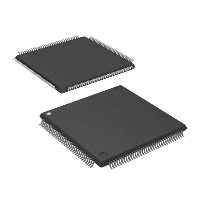


 工商网监
湘ICP备2023018690号
工商网监
湘ICP备2023018690号
